US8816263B2 - Vignetted planar spatial light-field sensor and spatial sampling designs for far-field lensless synthetic imaging via signal processing image formation - Google Patents
Vignetted planar spatial light-field sensor and spatial sampling designs for far-field lensless synthetic imaging via signal processing image formation Download PDFInfo
- Publication number
- US8816263B2 US8816263B2 US13/452,461 US201213452461A US8816263B2 US 8816263 B2 US8816263 B2 US 8816263B2 US 201213452461 A US201213452461 A US 201213452461A US 8816263 B2 US8816263 B2 US 8816263B2
- Authority
- US
- United States
- Prior art keywords
- light
- structures
- vignetted
- sensor
- tall
- Prior art date
- Legal status (The legal status is an assumption and is not a legal conclusion. Google has not performed a legal analysis and makes no representation as to the accuracy of the status listed.)
- Expired - Fee Related, expires
Links
- 238000003384 imaging method Methods 0.000 title claims abstract description 19
- 238000013461 design Methods 0.000 title description 32
- 238000005070 sampling Methods 0.000 title description 29
- 230000015572 biosynthetic process Effects 0.000 title description 11
- 238000012545 processing Methods 0.000 title description 6
- 238000000034 method Methods 0.000 claims abstract description 49
- 230000000007 visual effect Effects 0.000 claims abstract description 22
- 239000000463 material Substances 0.000 claims description 19
- 238000000638 solvent extraction Methods 0.000 claims description 3
- 238000005192 partition Methods 0.000 abstract 1
- 238000000926 separation method Methods 0.000 description 28
- 238000013459 approach Methods 0.000 description 25
- 230000006870 function Effects 0.000 description 18
- 230000003287 optical effect Effects 0.000 description 18
- 238000005259 measurement Methods 0.000 description 16
- 238000004458 analytical method Methods 0.000 description 13
- 238000004364 calculation method Methods 0.000 description 13
- 238000003491 array Methods 0.000 description 12
- 238000004519 manufacturing process Methods 0.000 description 11
- 238000013139 quantization Methods 0.000 description 10
- 230000008901 benefit Effects 0.000 description 8
- 230000008569 process Effects 0.000 description 7
- 230000005540 biological transmission Effects 0.000 description 6
- 238000004422 calculation algorithm Methods 0.000 description 5
- 230000000694 effects Effects 0.000 description 5
- 238000004891 communication Methods 0.000 description 4
- 230000002452 interceptive effect Effects 0.000 description 4
- 238000009877 rendering Methods 0.000 description 4
- 238000012800 visualization Methods 0.000 description 4
- 238000005457 optimization Methods 0.000 description 3
- 239000004065 semiconductor Substances 0.000 description 3
- 238000003860 storage Methods 0.000 description 3
- 230000032683 aging Effects 0.000 description 2
- 238000012512 characterization method Methods 0.000 description 2
- 238000004590 computer program Methods 0.000 description 2
- 238000011161 development Methods 0.000 description 2
- 230000018109 developmental process Effects 0.000 description 2
- 239000010410 layer Substances 0.000 description 2
- 239000011159 matrix material Substances 0.000 description 2
- 238000012986 modification Methods 0.000 description 2
- 230000004048 modification Effects 0.000 description 2
- 239000002365 multiple layer Substances 0.000 description 2
- 238000011002 quantification Methods 0.000 description 2
- 230000010076 replication Effects 0.000 description 2
- 238000007363 ring formation reaction Methods 0.000 description 2
- 230000035939 shock Effects 0.000 description 2
- PXFBZOLANLWPMH-UHFFFAOYSA-N 16-Epiaffinine Natural products C1C(C2=CC=CC=C2N2)=C2C(=O)CC2C(=CC)CN(C)C1C2CO PXFBZOLANLWPMH-UHFFFAOYSA-N 0.000 description 1
- RYGMFSIKBFXOCR-UHFFFAOYSA-N Copper Chemical compound [Cu] RYGMFSIKBFXOCR-UHFFFAOYSA-N 0.000 description 1
- 238000005452 bending Methods 0.000 description 1
- 230000015556 catabolic process Effects 0.000 description 1
- 238000006243 chemical reaction Methods 0.000 description 1
- 238000006731 degradation reaction Methods 0.000 description 1
- 238000001514 detection method Methods 0.000 description 1
- 238000005516 engineering process Methods 0.000 description 1
- 230000004907 flux Effects 0.000 description 1
- 239000011521 glass Substances 0.000 description 1
- 230000010365 information processing Effects 0.000 description 1
- 230000004807 localization Effects 0.000 description 1
- 239000000203 mixture Substances 0.000 description 1
- 239000013307 optical fiber Substances 0.000 description 1
- 238000000206 photolithography Methods 0.000 description 1
- 238000007639 printing Methods 0.000 description 1
- 230000001902 propagating effect Effects 0.000 description 1
- 238000002310 reflectometry Methods 0.000 description 1
- 238000011160 research Methods 0.000 description 1
- 230000003068 static effect Effects 0.000 description 1
- 238000006467 substitution reaction Methods 0.000 description 1
- XLYOFNOQVPJJNP-UHFFFAOYSA-N water Substances O XLYOFNOQVPJJNP-UHFFFAOYSA-N 0.000 description 1
Images


Classifications
-
- H—ELECTRICITY
- H01—ELECTRIC ELEMENTS
- H01L—SEMICONDUCTOR DEVICES NOT COVERED BY CLASS H10
- H01L27/00—Devices consisting of a plurality of semiconductor or other solid-state components formed in or on a common substrate
- H01L27/14—Devices consisting of a plurality of semiconductor or other solid-state components formed in or on a common substrate including semiconductor components sensitive to infrared radiation, light, electromagnetic radiation of shorter wavelength or corpuscular radiation and specially adapted either for the conversion of the energy of such radiation into electrical energy or for the control of electrical energy by such radiation
- H01L27/144—Devices controlled by radiation
- H01L27/146—Imager structures
- H01L27/14601—Structural or functional details thereof
- H01L27/14625—Optical elements or arrangements associated with the device
-
- H—ELECTRICITY
- H01—ELECTRIC ELEMENTS
- H01L—SEMICONDUCTOR DEVICES NOT COVERED BY CLASS H10
- H01L27/00—Devices consisting of a plurality of semiconductor or other solid-state components formed in or on a common substrate
- H01L27/14—Devices consisting of a plurality of semiconductor or other solid-state components formed in or on a common substrate including semiconductor components sensitive to infrared radiation, light, electromagnetic radiation of shorter wavelength or corpuscular radiation and specially adapted either for the conversion of the energy of such radiation into electrical energy or for the control of electrical energy by such radiation
- H01L27/144—Devices controlled by radiation
- H01L27/146—Imager structures
- H01L27/14683—Processes or apparatus peculiar to the manufacture or treatment of these devices or parts thereof
- H01L27/14685—Process for coatings or optical elements
Definitions
- This invention pertains to electronic image formation and refinement from overlapping measurement vignettes captured by an array of image sensors and associated vignetting micro-optics.
- the present invention is directed in major part to an alternate image formation system that combines readily-fabricated micro-optical structures, a two-dimensional image sensor array with electronic or digital image processing to actually construct the image.
- the present invention is directed to spatial aspects of light-field sensors, spatial signal design, spatial sub-sampling, and real-time computation for use with the systems and methods in the afore-listed patents and pending patent applications and other uses.
- Consideration is given to cases where the degree of sensor vignette capture overlap is very high, including cases at sensor-to-object separation distances where every, or nearly-every, sensor has at least some vignette capture overlap with the vignette capture of every, or nearly-every, other sensor. These conditions can occur, for example, for implementations employing planar image sensor arrays wherein
- Examples of interest include, for example, the use of a color LED (Light-Emitting Diode), color OLED (Light-Emitting Diode) display, color OLET (Light-Emitting Transistor) display, etc. for example in the form of a consumer television, and its use as an image sensor (for example, in professional and/or home video conferencing).
- a color LED Light-Emitting Diode
- color OLED Light-Emitting Diode
- OLET Light-Emitting Transistor
- relatively “tall” structures (which in some implementations can be light-emitting) and relatively “short” light-sensing structures can be fabricated in various types of arrays to create arrays of vignetted light sensors, the vignetted light sensors comprising a vignette depth resulting from the difference in height between the relatively “tall” structures and relatively “short” light-sensing structures.
- a method for implementing light field sensor for use in lensless synthetic imaging comprising:
- the “short” light-sensing structures can comprise organic photodiodes, OLEDs, or similar kinds of devices comprised of at least organic semiconducting material.
- the “tall” structure can comprise light-emitting elements.
- the “tall” structure can comprise can comprise one or more LEDs.
- the “tall” structure can comprise can comprise one or more OLEDs.
- the “tall” structure can comprise can comprise one or more OLETs.
- the “tall” structure can be a structure that does not emit light
- the “tall” structure can be a structure that does not emit light and comprise one or more electronic devices.
- the “tall” structure can be a structure that does not emit light and is non-electrical.
- staggered spatial decimation is used to reduce the number of measurement values involved in image formation calculations.
- the structures and their performance characterizations and tradeoffs as described thus far can be used to create various engineering designs for image capture.
- a given desired range of separation distances corresponding to “pitch” and resolution on a display
- associated vignette depths and % overlaps can be calculated.
- the % overlap quantity is used in spatial sub-sampling design.
- a resulting range of separation distances and % overlaps can be calculated.
- ranges of values of some of the design parameters p, d, L, and s, as well as other derived quantities such as % overlap and spatial sub-sampling design parameters are provided, ranges of values of the remaining design parameters and other derived quantities can be obtained employing formal Interval Analysis methods for calculation.
- ranges of values of some of the design parameters p, d, L, and s, as well as other derived quantities such as % overlap and spatial sub-sampling design parameters are provided, ranges of values of the remaining design parameters and other derived quantities can be obtained employing formal Interval Analysis methods for optimization.
- algorithm implementations are provided for modeling optical aspects of the above and related types of analysis.
- algorithm implementations are provided for interactive visualization modeling of optical aspects of the above and related types of analysis.
- a color LED (Light-Emitting Diode) array is used as an image sensor.
- a color LED (Light-Emitting Diode) display for example in the form of a consumer television, is used as an image sensor.
- a color OLED (Light-Emitting Diode) array is used as an image sensor.
- a color OLED (Light-Emitting Diode) display for example in the form of a consumer television, is used as an image sensor.
- a color OLET (Light-Emitting Transistor) array is used as an image sensor.
- a color OLET (Light-Emitting Transistor) display etc. for example in the form of a consumer television, is used as an image sensor.
- the resulting arrangement is used to capture the image of a relatively far-field object.
- the resulting arrangement is used as part of a video conferencing system.
- FIGS. 1 a - 1 d depict increasing degrees of overlap as the separation between a planar vignetted sensor array and an object plane increases.
- FIG. 2 depicts a high-level overview of synthetic image formation from overlapping-vignette light sensor array measurements as taught in issued patents U.S. Pat. No. 8,125,559 and CA 2,318,395 and pending patent applications U.S. Ser. Nos. 12/419,229; 12/828,280; 12/828,171; 12/828,207; 12/828,228; 13/072,588; and 13/180,345.
- FIGS. 3 a - 3 e depict color imaging approaches leveraging LED and OLED arrays as a color light field sensor as taught in U.S. Pat. No. 8,125,559 and pending patent applications U.S. Ser. Nos. 12/828,171; 12/828,207; 12/828,228; 13/072,588; and 13/180,345.
- FIG. 4 depicts additional color imaging approaches leveraging LED and OLED arrays as both a color display and a color light field sensor as taught in U.S. Pat. No. 8,125,559 and pending patent applications U.S. Ser. Nos. 12/828,171; 12/828,207; 12/828,228; 13/072,588; and 13/180,345.
- FIGS. 5 and 6 depict respectively example relative “tall” structures (which in some implementations can be light-emitting) and relative “short” light-sensing structures.
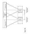
- FIG. 7 depicts four “short” light-sensing structures arranged in an open-interior ring formation.
- FIG. 8 depicts the arrangement of FIG. 7 wherein the four “short” light-sensing structures are fabricated in a ring surrounding “tall” structure (which in some implementations can be light-emitting).
- FIG. 9 depicts a linear arrangement of alternating short” light-sensing structures and “tall” structures (which in some implementations can be light-emitting).
- FIG. 10 depicts a plurality of parallel-oriented instances of the linear arrangement of FIG. 9 , each parallel-oriented instance separated by a linear arrangement comprising only “short” light-sensing structures.
- FIG. 11 a depicts a plurality of only parallel-oriented instances of the linear arrangement of FIG. 9 , each parallel-oriented instance alternately staggered so as to create cavities surrounded on all sides by “tall” structures (which in some implementations can be light-emitting), the bottom of each cavity comprising a “short” light-sensing structure.
- FIG. 11 b depicts the example pattern of FIG. 11 a extended to an example of larger-scale replication.
- FIG. 12 depicts how a vignette structure can limit the range of incident angles at which rays of light within a light field are able to reach the surface of the light-sensing element within the vignetting structure.
- FIG. 13 depicts a representation of the refractive effect (governed by Snell's law) that is created at the interface between two materials with differing indices of refraction in the usual fashion it which it is described in textbooks.
- FIG. 14 depicts the relation of FIG. 13 with light traveling in the opposite direction showing light rays will travel along the same path as in FIG. 13 .
- FIG. 15 a depicts an interface between pairs of materials with differing indices of refraction can be implemented at the top of the vignetting structure.
- FIG. 15 b depicts an interface between pairs of materials with differing indices of refraction can be implemented both within and at the top of the vignetting structure.
- FIG. 16 depicts an optical ray-tracing model for a pair of example sensors, each provided with an associated vignetting structure, the vignetting structures aligned in parallel in a planar arrangement.
- FIG. 17 depicts paths of the extremal light rays defining the span of light capture from the vignetted sensor, as in FIG. 12 , but with dimensions added and an observed planar object located a distance L from the surface of the vignetted light sensor.
- FIG. 18 a depicts two vignetting structures side-by-side in the same plane with centers separated by the distance
- FIG. 18 b depicts an application of the arrangement of FIG. 18 a wherein the centerlines of each sensor are brought forward to intersect an observed object place a distance L from the sensor array plane.
- FIG. 19 a depicts a variation on the arrangement depicted in FIG. 18 a wherein the separation distance L between the sensor plane and the object is large enough that the vignetted sensor capture ranges overlap.
- FIG. 19 b depicts a variation on the arrangement depicted in FIG. 18 b wherein the separation distance L between the sensor plane and the object is large enough that the vignetted sensor capture ranges overlap.
- FIG. 19 c depicts a quantification of the capture overlap range.
- the overlap occurs within the region in parallel projection to the sensor separations, the sensor centers separated by distance s.
- FIG. 20 a depicts an optical ray-tracing model for relating the image capture width at a given distance L to the monitor width w.
- FIG. 20 b depicts an optical ray-tracing model for relating the image capture height at a given distance L to the monitor height h.
- vignetted light sensors can be used to create synthetic images via algebraic operations.
- the algebraic operations which can comprises for example a predetermined generalized-inverse operation responsive to a Depth-of-Field parameter.
- the generalized-inverse operation (for example, a Moore-Penrose generalized-inverse) is used to recover estimated pixel light amplitude at a particular distance from the vignetted light sensor surface.
- the generalized-inverse operation effectively solves an (over-specified) set of M equations for a “best fit” of N unknowns, with integers M>N (more equations than unknowns).
- the “best fit” (for example, in a “least-squares” sense for the Moore-Penrose generalized-inverse) provides robustness against deviant measurements as can arise from manufacturing variations, variations due to aging, thermal expansion, moderate physical shock, etc.
- FIGS. 1 a - 1 d depict increasing degrees of overlap as the separation between a planar vignetted sensor array and an object plane increases.
- the generalized-inverse operation has to “work harder” to recover the estimated pixel light amplitude values from the measurements, and is more susceptible to noise errors, computational rounding errors, etc.
- FIG. 1 a At one extreme of operating range of separation distance ( FIG. 1 a ), there is no overlap and the generalized-inverse operation is effectively a trivial identity operation (albeit with less of the aforementioned robustness features).
- FIG. 1 d At the opposite extreme of operating range of separation distance ( FIG. 1 d ), there is nearly 100% overlap and the generalized-inverse operation has to (numerically) work extremely hard to create the estimated pixel light amplitude values from the measurements and can be vulnerable to noise errors, computational rounding errors, etc.
- FIG. 2 depicts a high-level overview of synthetic image formation from overlapping-vignette light sensor array measurements, leveraging the above, as taught in issued patents U.S. Pat. No. 8,125,559 and CA 2,318,395 and pending patent applications U.S. Ser. Nos. 12/419,229; 12/828,280; 12/828,171; 12/828,207; 12/828,228; 13/072,588; and 13/180,345.
- FIGS. 3 a - 3 e depict color imaging approaches leveraging LED and OLED arrays as a color light field sensor as taught in U.S. Pat. No. 8,125,559 and pending patent applications U.S. Ser. Nos. 12/828,171; 12/828,207; 12/828,228; 13/072,588; and 13/180,345.
- FIG. 4 depicts additional color imaging approaches leveraging LED and OLED arrays as both a color display and a color light field sensor as taught in U.S. Pat. No. 8,125,559 and pending patent applications U.S. Ser. Nos. 12/828,171; 12/828,207; 12/828,228; 13/072,588; and 13/180,345.
- FIGS. 5 and 6 depict respectively example relative “tall” structures (which in some implementations can be light-emitting) and relative “short” light-sensing structures.
- Such structures can internally comprise a plurality of layers and can accordingly be fabricated by traditional semiconductor photolithography fabrication techniques, functional printing fabrication techniques, etc.
- the “short” light-sensing structures can comprise organic photodiodes, OLEDs, or similar kinds of devices comprised of at least organic semiconducting material.
- the “tall” structure can comprise light-emitting and can comprise one or more OLEDs.
- the “tall” structure can comprise can comprise one or more LEDs.
- the “tall” structure can comprise can comprise one or more OLEDs.
- the “tall” structure can comprise can comprise one or more OLETs.
- the “tall” structure can be a structure that does not emit light
- the “tall” structure does not emit light.
- the “tall” structure comprises one or more electronic devices.
- the one or more electronic devices can include one or more of a driving transistor, a sensor interface transistor, and a multiplexing transistor.
- the “tall” structure can be a structure that does not emit light and is non-electrical.
- Such relatively “tall” structures (which in some implementations can be light-emitting) and relatively “short” light-sensing structures can be fabricated in various types of arrays comprising adjacent or near-adjacent placement of the structures. For example:
- patterns such as that rendered in arrangements such as that of FIG. 11 a , i.e., pattern comprising cavities surrounded on all sides by “tall” structures (which in some implementations can be light-emitting), the bottom of each cavity comprising one or more “short” light-sensing structures.
- Arrangements comprising such patterns implement light-sensing structures that present the surface of a light-sensing element at the bottom of a vignetting structure.
- the depth of the vignetting structure is the difference in “height” between the “short” light-sensing structures and the “tall” structures (which in some implementations can be light-emitting).
- the pattern of FIG. 11 a can ready be extended to larger-scale replication as suggested in FIG. 11 b.
- relatively “tall” structures (which in some implementations can be light-emitting) and relatively “short” light-sensing structures can be fabricated in various types of arrays to create arrays of vignetted light sensors, the vignetted comprising a vignette depth resulting from the difference in height between the relatively “tall” structures and relatively “short” light-sensing structures.
- the “tall” structures comprise light-emitting elements, and the array of “tall” structures collectively act as a light-emitting visual display further comprising an array of vignetted light sensors, each vignetted light sensor comprising at least one “short” structure.
- electronic circuitry interfacing and/or driving the light-emitting elements can be configured in various types of multiplexed array arrangements configured for multiplexing operation.
- each vignetted light sensor provides a measurable electrical quantity responsive to the light it receives from incoming light not occluded by the vignette.
- the measurable electrical quantity can comprise a photocurrent, a photovoltage, or a photo-induced charge, each of which can be converted responsively into an electrical signal by simple electronic circuitry.
- electronic circuitry can be configured in a multiplexed array.
- Each vignette structure can limit the range of incident angles at which rays of light within a light field are able to reach the surface of the light-sensing element within the vignetting structure. This is illustrated in FIG. 12 .
- the dashed lines denote light ray paths at limiting angles via which the rays can travel to the light sensor positioned at the base of the depicted vignetting structure.
- the light capture range expands as a linear (affine, i.e., proportional term plus offset term) function of the distance from the surface of the sensor.
- the extremal light rays defining the span of light capture intersect begin at a depth halfway down the vignetting structure path, more precisely halfway between the opening of the vignette and the surface of the light sensor at the base of the vignetting structure.
- the arrangements can be fabricated so that the sides of the vignetting structure cavity do not reflect light. In other embodiments, the arrangements can be fabricated so that the sides of the vignetting structure cavity do advantageously reflect light.
- the reflectivity can alter the range of incident angles at which rays of light within a light field are able to reach the surface of the light-sensing element within the vignetting structure.
- a reflective vignetting structure interior would broaden the light capture range with respect to what the light capture range would be with a non-reflective vignetting structure interior. This is because light that would not otherwise be able to travel to the sensor directly would reflect from the walls of the vignetting structure interior one or more times, and typically at least some portion, and in some arrangements a significant amount, of this reflected light would travel to the sensor.
- Another method of broadening the vignette span is to leverage the Snell's law refractive effect created at the interface between two materials with differing indices of refraction. This is effect is depicted in FIG. 13 in the usual fashion it which it is described in textbooks (i.e., light travelling from air or vacuum into the surface of a material such as glass or water.
- the light ray paths depicted in FIG. 12 can be bent in angles prescribed by Snell's law.
- such an interface between air and one or more layers of materials with differing indices of refraction can be implemented at least in part at the top of the vignetting structure.
- the simplest case of this is filing the entire vignetting structure with a single material having an index of refraction significantly differing from that of air, for example as depicted in FIG. 15 a .
- adjoining pairs of materials can be entirely localized at the top of the vignetting structure.
- the interface between one or more pairs of materials with differing indices of refraction can be implemented within the vignetting structure, for example as in the single-pair structure depicted in FIG. 15 b.
- the capture range can be broadened with respect to how it would occur in the arrangement of FIG. 12 ; here the capture range broadening for the sensor and vignette structure is accomplished without the use of reflective surfaces within the interior of the vignette structure.
- a narrowing of the capture range can be of interest since any such narrowing reduces the extent of overlap as the separation distance between the sensor array and object increases to integer multiples of the width and/or height of sensor array.
- attempts to attain a narrowing of the capture range simply from adjustment of the depth of the vignetting structures tends to require deeper vignettes, and increasingly deeper vignetting structures can become increasingly difficult to fabricate at a given level of precision.
- a method for implementing light field sensor for use in lensless synthetic imaging comprising:
- a visual display monitor As an example of a visual display monitor, consider a visual display monitor as can be found in a home television viewing room or videoconferencing room:
- computer monitors often have yet other aspect ratios (such as 1024 ⁇ 1280 monitors having an aspect ratio of 4:5), NTSC video monitors have an aspect ratio of 3:4, etc.
- aspect ratios for example, as in smart phones, tablet computers, laptop computers, etc.
- sensor shapes can also be supported by the invention using the general schemes presented in the sections to follow.
- the sensor array (or visual display monitor including the sensor array) is assumed flat and all sensors are assumed pointing perpendicularly outward from the surface of the screen. This case is of interest as most contemporary monitors are flat and this case also invokes limitations of the localization of vignette capture range overlap among sensors in the sensor array.
- other sensor orientation arrangements for example curved arrangements, can improve the performance beyond that described herein.
- FIG. 16 depicts an optical ray-tracing model for a pair of example sensors, each provided with an associated vignetting structure, the vignetting structures aligned in parallel.
- Other arrangements can be used and this arrangement is merely by way of example and is not restrictive of the invention.
- the following physical length parameters are indicated:
- the extreme-range light rays cross midway up the light-travel depth of the vignetting structure.
- the extremal light rays defining the span of light capture from the vignetted light sensor effectively begin at a depth d/2 beneath the opening of the vignette, where d is the depth of the vignetting structure (more precisely, the distance between the surface of the light sensor and the opening at the opposite end of the vignetting structure.
- FIG. 17 depicts the paths of the extremal light rays defining the span of light capture from the vignetted sensor, as in FIG. 12 , but with dimensions added and an observed planar object located a distance L from the surface of the vignetted light sensor.
- the span of light capture from the vignetted light sensor will be a function of d, p, and L; for convenience the function will be called
- the large isosceles triangle depicted in FIG. 17 comprising the top portion of length to be given by the function vspan[L,d,p] and comprising opposing vertex at a point halfway through the vignetting structure, is a similar triangle to the far smaller isosceles triangle with top edge of width p and depth d/2 that is wholly contained within the top half of the vignetting structure.
- the other two sides of the large isosceles triangle have length (L+d/2).
- the function vspan[L,d,p] can be solved for using the proportions determined by similar triangles, resulting in the expression
- FIG. 18 a depicts two vignetting structures side-by-side in the same plane with centers separated by the distance s.
- FIGS. 18 a - 18 b the separation distance between the sensor plane an the object plane is small enough that there is no overlap in the capture vignettes of two widely-spaced sensors.
- FIGS. 19 a - 19 c to be considered in detail shortly, provide a related development for cases where the separation distance between the sensor plane and the object plane is large enough that there is overlap in the capture vignettes of two widely-spaced sensors.
- FIG. 20 a depicts an optical ray-tracing model for relating the image capture width at a given distance L to the monitor width w.
- FIG. 20 b depicts an optical ray-tracing model for relating the image capture height at a given distance L to the monitor height h.
- optical ray tracing processes to be described below are identical for width or height. They can be generalized, then, by using the term “monitor dimension.” Within this dimension, subportions will be called “regions”—for example the general term “image capture region” generalizes “image capture width” and “image capture height,” and the general term “image overlap region” generalizes “image overlap width” and “image overlap height.”
- FIG. 18 b depicts an application of the arrangement of FIG. 18 a wherein the centerlines of each sensor are brought forward to intersect an observed object place a distance L from the sensor array plane.
- the image capture range of each vignetted sensor extends a distance of 1 ⁇ 2 vspan[L,d,p] to the left or right of its centerline.
- the image capture range spanned by an array of sensors whose edge sensors are separated by a distance s (between the edge sensor centerlines) would be given by 1 ⁇ 2 vspan[L,d,p]+s+1 ⁇ 2 vspan[L,d,p]. which simplifies to s+1 ⁇ 2 vspan[L,d,p], or
- the image capture region size is given by
- image capture region will be linear in the separation distance L between the sensor plane and the object.
- This range of vignetting structure depth is fortuitous as a vignetting structure that is deeper that ⁇ 4 times the pixel width can become somewhat difficult to fabricate with precision. Recall, however, that the Snell's Law ray bending approach described earlier can be used to create optical equivalents to deep vignette cavities.
- FIG. 19 a depicts a variation on the arrangement depicted in FIG. 18 a wherein the separation distance L between the sensor plane and the object is large enough that the vignetted sensor capture ranges overlap.
- FIG. 19 b depicts a variation on the arrangement depicted in FIG. 18 b wherein the separation distance L between the sensor plane and the object is large enough that the vignetted sensor capture ranges overlap.
- the geometry and math is the same as for the arrangement depicted in FIG. 18 b , so the image capture range is the same, namely given by 1 ⁇ 2 vspan[L,d,p]+s+1 ⁇ 2 vspan[L,d,p]. which simplifies to s+1 ⁇ 2 vspan[L,d,p], or
- FIG. 19 c depicts a quantification of the capture overlap range.
- the sensor array is assumed flat and all sensors are assumed pointing perpendicularly outward from the surface of the array. As noted earlier, other sensor orientation arrangements can improve the performance beyond that described above.
- the invention provides for staggered spatial decimation (sub-sampling) to be used to reduce the number of measurement values involved in image formation calculations.
- the wide degree of vignette overlap implies that the immediate vignetted sensor neighbors of any given vignetted sensor measures practically the same light flux as the given vignetted sensor itself.
- the number of measurement values involving in the calculation of the value of a specified output pixel can be reduced by only incorporating the measurement values for every N th sensor in the index directions surrounding it.
- a thinned collection of sensor values could be for example those in the sequence: ⁇ 1,1 ⁇ , ⁇ 1,3 ⁇ , ⁇ 3,1 ⁇ , ⁇ 3,3 ⁇ , ⁇ 3,5 ⁇ , ⁇ 5,3 ⁇ , ⁇ 5,5 ⁇ , . . . or the sequence ⁇ 2,2 ⁇ , ⁇ 2,4 ⁇ , ⁇ 4,2 ⁇ , ⁇ 4,4 ⁇ , ⁇ 4,6 ⁇ , ⁇ 6,4 ⁇ , ⁇ 6,6 ⁇ , . . .
- a thinned collection of sensor values could be for example those in the sequence: ⁇ 1,1 ⁇ , ⁇ 1,4 ⁇ , ⁇ 4,1 ⁇ , ⁇ 4,4 ⁇ , ⁇ 4,7 ⁇ , ⁇ 7,4 ⁇ , ⁇ 7,7 ⁇ , . . . or the sequence ⁇ 2,2 ⁇ , ⁇ 2,5 ⁇ , ⁇ 5,2 ⁇ , ⁇ 5,5 ⁇ , ⁇ 5,8 ⁇ , ⁇ 8,5 ⁇ , ⁇ 8,8 ⁇ , . . . or the sequence ⁇ 3,3 ⁇ , ⁇ 3,6 ⁇ , ⁇ 6,3 ⁇ , ⁇ 6,6 ⁇ , ⁇ 6,9 ⁇ , ⁇ 9,6 ⁇ , ⁇ 9,9 ⁇ , . . .
- the indices of the thinned collection used in the previous output pixel would be shifted by 1 for that index.
- the spatial resolution of the synthetically-formed image is not affected by this staggered spatial decimation (sub-sampling) employed in reducing the complexity of the value calculation of each individual output pixel.
- the real-time computational load scales linearly with the number of pixels of resolution of the captured image (maximum resolution bounded by the number of sensors in the sensor array).
- the staggered spatial sub-sampling is robustly supported for at least a 1/10—rate since the vignette overlap (i.e., roughly on the order of 1000 pixels) is so significant.
- the impact is so significant.
- vignette overlap for a screen-to-object separation distance of 8 feet is so significant (i.e., roughly on the order of 1000 pixels), in many applications a 1/64—rate staggered sub-sampling (if not sparser rate staggered sub-sampling) would be robustly supported.
- the invention provides for the implementations of interactive visualization and mathematical analysis software tool for performing the optical aspects of the above and related types of analysis.
- sensor[c, L, d, p] Graphics[ ⁇ LightBlue, Rectangle[ ⁇ 0, c ⁇ p/2 ⁇ , ⁇ d, c + p/2 ⁇ ] ⁇ , Line[ ⁇ 0, c ⁇ p/2 ⁇ , ⁇ d + L, c ⁇ p/2 + (p/d) (d + L) ⁇ ], Line[ ⁇ 0, c + p/2 ⁇ , ⁇ d + L, c + p/2 ⁇ (p/d) (d + L) ⁇ ] ⁇ ]
- the output is a parameterized visual graphics rendering of a sensor vignette structure (of the specified depth d and sensor center-location c) together with the envelope of the resulting light-capture vignette (extending to the specified screen-to-object separation distance L).
- the output is a parameterized visual graphics rendering of a parallel object plane (located at specified screen-to-object separation distance L) aligned & scaled along with the above sensor.
- Each sensor can render its own object plane, and a linear array of sensors creates a merged object plane.
- vignettespan[ c,L,d,p] ⁇ c+p/ 2 ⁇ ( p/d )( d+L ), c ⁇ p/ 2+( p/d )( d+L ) ⁇
- c is the center of the sensor in one-dimention of a sensor array.
- the output is a list of the extreme values of the light sensing envelope. The most positive value is the first element vignettespan[c,L,d,p][[1]] and the most negative value is the second element vignettespan[c,L,d,p][[2]].
- overlap[c, L, d, p] Max[0, (vignettespan[ ⁇ c, L, d, p][[2]] ⁇ vignettespan[c, L, d, p][[1]]) / (vignettespan[c, L, d, p][[2]] ⁇ vignettespan [c, L, d, p][[1]]) ]
- the output is a scalar representing the spatial overlap of the light sensing envelope of two sensors symmetrically spaced either side of a central reference position.
- the scale of the spacing is used to represent the spacing of adjacent sensors.
- captureregion[ c,L,d,p ] vignettespan[ c,L,d,p][[ 2]] ⁇ vignettespan[ ⁇ c,L, d,p][[ 1]]
- the output is a scalar representing the region of the overall image sensing envelope of two sensors symmetrically spaced either side of a central reference position.
- the described techniques can be implemented as a method, apparatus or article of manufacture involving software, firmware, micro-code, hardware such as logic, memory and/or any combination thereof.
- article of manufacture refers to code or logic and memory implemented in a medium, where such medium can include hardware logic and memory [e.g., an integrated circuit chip, Programmable Gate Array (PGA), Application Specific Integrated Circuit (ASIC), etc.] or a computer readable medium, such as magnetic storage medium (e.g., hard disk drives, floppy disks, tape, etc.), optical storage (CDROMs, optical disks, etc.), volatile and non-volatile memory devices [e.g., Electrically Erasable Programmable Read Only Memory (EEPROM), Read Only Memory (ROM), Programmable Read Only Memory (PROM), Random Access Memory (RAM), Dynamic Random Access Memory (DRAM), Static Random Access Memory (SRAM), flash, firmware, programmable logic, etc.].
- EEPROM Electrically Erasable Programmable Read Only Memory
- ROM Read Only Memory
- PROM
- Code in the computer readable medium is accessed and executed by a processor.
- the medium in which the code or logic is encoded can also include transmission signals propagating through space or a transmission media, such as an optical fiber, copper wire, etc.
- the transmission signal in which the code or logic is encoded can further include a wireless signal, satellite transmission, radio waves, infrared signals, Bluetooth, the internet etc.
- the transmission signal in which the code or logic is encoded is capable of being transmitted by a transmitting station and received by a receiving station, where the code or logic encoded in the transmission signal can be decoded and stored in hardware or a computer readable medium at the receiving and transmitting stations or devices.
- the “article of manufacture” can include a combination of hardware and software components in which the code is embodied, processed, and executed.
- the article of manufacture may include any information bearing medium.
- the article of manufacture includes a storage medium having stored therein instructions that when executed by a machine results in operations being performed.
- Certain embodiments can take the form of an entirely hardware embodiment, an entirely software embodiment or an embodiment containing both hardware and software elements.
- One embodiment may be implemented in software, which includes but is not limited to firmware, resident software, microcode, etc.
- Elements that are in communication with each other need not be in continuous communication with each other, unless expressly specified otherwise.
- elements that are in communication with each other may communicate directly or indirectly through one or more intermediaries.
- a description of an embodiment with several components in communication with each other does not imply that all such components are required. On the contrary, a variety of optional components are described to illustrate the wide variety of possible embodiments.
- processes and methods may be described in a sequential order, such processes, methods and algorithms may be configured to work in alternate orders. In other words, any sequence or order of blocks that may be described does not necessarily indicate a requirement that the blocks be performed in that order.
- the processes described herein may be performed in any order practical. Further, some processes may be performed simultaneously, in parallel, or concurrently. Further, some or all processes may be performed in run-time mode.
- Computer program means or computer program in the present context mean any expression, in any language, code or notation, of a set of instructions intended to cause a system having an information processing capability to perform a particular function either directly or after either or both of the following a) conversion to another language, code or notation; b) reproduction in a different material form.
Landscapes
- Physics & Mathematics (AREA)
- Engineering & Computer Science (AREA)
- Power Engineering (AREA)
- Electromagnetism (AREA)
- Condensed Matter Physics & Semiconductors (AREA)
- General Physics & Mathematics (AREA)
- Computer Hardware Design (AREA)
- Microelectronics & Electronic Packaging (AREA)
- Solid State Image Pick-Up Elements (AREA)
Abstract
Description
-
- U.S. Pat. No. 8,125,559;
- CA 2,318,395
- PCT/US99/01789;
- U.S. Ser. No. 12/419,229;
- U.S. Ser. No. 12/828,280;
- U.S. Ser. No. 12/828,171;
- U.S. Ser. No. 12/828,207;
- U.S. Ser. No. 12/828,228;
- U.S. Ser. No. 13/072,588;
- U.S. Ser. No. 13/180,345.
-
- The planar image sensor arrays has high spatial resolution;
- The vignette-based imaging is of a relatively far-field object;
- Both of the above at once.
-
- Fabrication relatively tall structures and short structures, wherein the short structures comprise light sensing capabilities, and wherein the tall structures and short structures are arranged in an array to create an array comprising a plurality of vignetted light sensors, and
- Receiving an incoming light field,
- Partitioning the incoming light with the tall structures to created a plurality of vignetted light fields, each vignetted light field uniquely associated with a particular vignetted light sensor from the plurality of vignetted light sensors,
- Receiving each vignetted light field at the associated each vignetted light sensor, and
- Generating, at each vignetted light sensor, a measurable electrical quantity responsive to the associated vignetted light field,
wherein the vignetted light sensors comprising a vignette depth resulting from the difference in height between the tall structures and short light-sensing structures, and wherein the collection of the electrical quantities from each of the vignetted light sensors is responsive to the received incoming light field.
-
- First, light-field sensor arrangements compatible with visual display monitors (such as can be used with home television displays, video conferencing systems, computer monitors, smart phones, laptop computers, computer tablets, and other devices) are briefly considered;
- Next a general geometric framework is assembled for calculating the size and span of the sensor vignettes as a function of vignetting structure parameters and the separation distance between the visual display screen and imaged object;
- Then the image capture region (of the width or the height of the visual display screen) as a function of these parameters and the visual display screen dimension (width or height);
- Using a related calculation, the degree of sensor vignetting overlap can be calculated;
- For parameter ranges pertaining to regions viable for example use in home television viewing areas or video conferencing rooms, examples are given where the degree of sensor vignette overlap is determined to be high enough to not impose resolution degradation and also high enough to support spatial sub-sampling;
- Spatial sub-sampling is then considered;
- Consideration is then directed to calculation-imposed quantization noise and the available dynamic range above the noise floor for various levels of signal processing arithmetic accuracy;
- Consideration is also directed to the computational load captured image resolution;
- Some examples are provided;
- Example mathematical analysis and interactive visualization software to assist in design and research is then described.
Creation of Vignette Structures for Light Detection within Displays or Other Fabricated Surfaces
-
-
FIG. 7 depicts four “short” light-sensing structures arranged in an open-interior ring formation; -
FIG. 8 depicts the arrangement ofFIG. 7 wherein the four “short” light-sensing structures are fabricated in a ring surrounding “tall” structure (which in some implementations can be light-emitting); -
FIG. 9 depicts a linear arrangement of alternating short” light-sensing structures and “tall” structures (which in some implementations can be light-emitting); -
FIG. 10 depicts a plurality of parallel-oriented instances of the linear arrangement ofFIG. 9 , each parallel-oriented instance separated by a linear arrangement comprising only “short” light-sensing structures; -
FIG. 11 a depicts a plurality of only parallel-oriented instances of the linear arrangement ofFIG. 9 , each parallel-oriented instance alternately staggered so as to create cavities surrounded on all sides by “tall” structures (which in some implementations can be light-emitting), the bottom of each cavity comprising a “short” light-sensing structure.
-
-
- Fabrication relatively tall structures and short structures, wherein the short structures comprise light sensing capabilities, and wherein the tall structures and short structures are arranged in an array to create an array comprising a plurality of vignetted light sensors, and
- Receiving an incoming light field,
- Partitioning the incoming light field with the tall structures to created a plurality of vignetted light fields, each vignetted light field uniquely associated with a particular vignetted light sensor from the plurality of vignetted light sensors,
- Receiving each vignetted light field at the associated each vignetted light sensor, and
- Generating, at each vignetted light sensor, a measurable electrical quantity responsive to the associated vignetted light field,
wherein the vignetted light sensors comprising a vignette depth resulting from the difference in height between the tall structures and short light-sensing structures, and wherein the collection of the measurable electrical quantities from each of the vignetted light sensors is responsive to the received incoming light field.
Example Visual Display Monitor Parameters
-
- 1,000,000 pixels
- 1 mm pixel pitch
-
- a
square monitor 1000 mm×1000 mm (3.3 feet×3.3 feet) - a 16:9 monitor of 1333 mm×750 mm (4.4 feet×2.5 feet)
- a
| Variable | Description | Example |
| p | Sensor pixel size diameter/side | Example: p = 1 |
| (“1 mm pitch”) | ||
| d | Vignette depth | d = p, d = 4p, etc. |
| L | Separation of object from observing | |
| plane of planar vignetted light-sensor | ||
| surface | ||
| c | Sensor center (as indexed in an array) | Position/iterated |
| over lattice | ||
| s | Separation between the ceneters of a | general cases, |
| pair of vignetted light-sensors | including far extremes | |
| of an array | ||
½ vspan[L,d,p]+s+½ vspan[L,d,p].
which simplifies to s+½ vspan[L,d,p], or
-
- For vignette depth d=1 the capture region at 8 feet is 5880 mm (19.3 feet wide)
- For vignette depth d=2 the capture region at 8 feet is 3440 mm (11.3 feet wide)
- For vignette depth d=3 the capture region at 8 feet is 2630 mm (8.6 feet wide)
- For vignette depth d=4 the capture region at 8 feet is 2220 mm (7.3 feet wide)
- For vignette depth d=5 the capture region at 8 feet is 1980 mm (6.5 feet wide)
-
- For vignette depth d=1 the capture region at 8 feet is 6220 mm (20.4 feet wide)
- For vignette depth d=2 the capture region at 8 feet is 3780 mm (12.4 feet wide)
- For vignette depth d=3 the capture region at 8 feet is 2960 mm (9.7 feet wide)
- For vignette depth d=4 the capture region at 8 feet is 2560 mm (8.4 feet wide)
- For vignette depth d=5 the capture region at 8 feet is 2310 mm (7.6 feet wide)
-
- The likely deepest vignetting structure for use with a 1000 mm to 1333 mm wide visual display screen is d=4 (so as to avoid too narrow a capture region);
- The likely shallowest vignetting structure for use with a 1000 mm to 1333 mm wide visual display screen is d=2 (so as to avoid too wide a capture region).
½ vspan[L,d,p]+s+½ vspan[L,d,p].
which simplifies to s+½ vspan[L,d,p], or
Of course this quantity is equal to
this form of the expression to be appreciated in a moment
½ vspan[L,d,p]+½ vspan[L,d,p].
½ vspan[L,d,p]+½ vspan[L,d,p].
exceeds the value of s. Therefore capture overlap range is given by
½ vspan[L,d,p]+½ vspan[L,d,p]−s
which simplifies to
vspan[L,d,p]−s
and thus for values of L>L* there will be capture overlap. Again note that if L=L* then
so that the value of capture overlap range is
Is negative; this fact will be used below in a moment.
and the image capture range is given by
then the %-overlap (for case where L>L*) is given by
is always positive, the ratio expression for the %-overlap is only negative for cases where L<L*. Thus, for all values of L (that is, all values with L>0), the general expression for the %-overlap is given by
-
- From a provided pixel width p (corresponding to “pitch” and resolution on a display), a given desired range of separation distances Lmin, >L>Lmax, and a given screen size (determining the largest value for s), associated vignette depths d and % overlaps can be calculated. The % overlap can be then used in spatial sub-sampling design using approaches such as those described in the section to follow (as well as other spatial sub-sampling design approaches).
- From a provided pixel width p (corresponding to “pitch” and resolution on a display), a given screen size (determining the largest value for s), and a practical range of inexpensively and reliably fabricated vignette depths dmin>d>dmax, a resulting range of separation distances Lmin>L>Lmax and overlaps can be calculated. The % overlap can be then used in spatial sub-sampling design using approaches such as those described in the section to follow (as well as other spatial sub-sampling design approaches).
- From a maximum permitted % overlap, and other values or ranges for some of the design parameters p, d, L, and s, values or ranges for the remaining design parameters can be calculated.
- These are but a few of representative examples. In general, fixed values and/or ranges of values of some of the design parameters p, d, L, and s, as well as other derived quantities such as % overlap and spatial sub-sampling design parameters (for example, as described below), can be used to determine fixed values and/or ranges of values of the remaining design parameters and other derived quantities.
-
- Introduction To Interval Analysis by Ramon E. Moore, R. Baker Kearfott, and Michael J. Cloud, ISBN 0898716696, published 1998-2008 by the Society For Industrial And Applied Mathematics (SIAM), Philadelphia;
- Methods And Applications Of Interval Analysis by Ramon E. Moore, ISBN 0898711614, published in 1979 by the Society For Industrial and Applied Mathematics, Philadelphia;
- Applied Interval Analysis by Luc Jaulin, Michel Kieffer, Olivier Didrit, and Eric Walter, ISBN 1852332190, published 2001 by Springer, London;
- Global Optimization Using Interval Analysis: Revised and Expanded by Eldon Hansen, ISBN 0824740599, published in 2003 by Marcel Dekker/CRC Press.
Synthetic Imaging Computation Considerations
-
- For a case where 1000×1000 pixel resolution is desired: on the order of 1000×1000=1,000,000 linear calculations will be performed (using geometric and sparse-matrix techniques in a 4-D tensor structure) comprising linear operations involving sums and differences of on the order of 1,000,000 numbers. Sums of 1,000,000 binary numbers require up to Log 2(1,000,000)=20 bits. Then:
- Use of 32-bit arithmetic leaves 12 bits to accommodate both sensor-value dynamic range and the impact of quantization noise (possibly not enough).
- Use of 48-bit arithmetic leaves 28 bits to accommodate both sensor-value dynamic range and the impact of quantization noise.
- Use of 64-bit arithmetic leaves 44 bits to accommodate both sensor-value dynamic range and the impact of quantization noise.
- For a case where 1000×1000 pixel resolution is desired: on the order of 1000×1000=1,000,000 linear calculations will be performed (using geometric and sparse-matrix techniques in a 4-D tensor structure) comprising linear operations involving sums and differences of on the order of 1,000,000 numbers. Sums of 1,000,000 binary numbers require up to Log 2(1,000,000)=20 bits. Then:
-
- For a case where 500×500 pixel resolution is desired: on the order of 500×500=250,000 linear calculations will be performed (using geometric and sparse-matrix techniques in a 4-D tensor structure) comprising linear operations involving sums and differences of on the order of 250,000 numbers. Sums of 250,000 binary numbers require up to Log2(250,000)=18 bits. In bold terms, one could expect worse-case quantization noise to consume up to another 18 bits. Thus, the 500×500 pixel resolution case is not appreciably different from the number of bits required (basically ˜4 bits), although now as much as 12 bits of combined dynamic range and noise margin could be accommodated.
{1,1},{1,3},{3,1},{3,3},{3,5},{5,3},{5,5}, . . .
or the sequence
{2,2},{2,4},{4,2},{4,4},{4,6},{6,4},{6,6}, . . .
{1,1},{1,4},{4,1},{4,4},{4,7},{7,4},{7,7}, . . .
or the sequence
{2,2},{2,5},{5,2},{5,5},{5,8},{8,5},{8,8}, . . .
or the sequence
{3,3},{3,6},{6,3},{6,6},{6,9},{9,6},{9,9}, . . .
-
- For 1/11—rate staggered spatial sub-sampling, the number of measurement values involved in the aforementioned linear operation sums and differences will drop by a factor of 11×11=121, representing a savings of 7 bits. Allowing then 20−7=13 bits plus another 13 bits for quantization noise, use of 32-bit arithmetic leaves 32−26=6 bits of dynamic range.
- For 1/16—rate staggered spatial sub-sampling, the number of measurement values involved in the aforementioned linear operation sums and differences will drop by a factor of 16×16=256, representing a savings of 8 bits. Allowing then 20−8=12 bits plus another 12 bits for quantization noise, use of 32-bit arithmetic leaves 32−24=8 bits of dynamic range.
- For 1/64—rate staggered spatial sub-sampling, the number of measurement values involved in the aforementioned linear operation sums and differences will drop by a factor of 32×32=1024, representing a savings of 8 bits. Allowing then 20-8=12 bits plus another 12 bits for quantization noise, use of 32-bit arithmetic leaves 32−24=8 bits of dynamic range.
-
- The resolution is therefore defined by the computational and measurement noise floor;
- The real-time computation can work with a considerably large degree of staggered spatial sub-sampling, dramatically reducing the number of linear operations required of the real-time processor;
- Such staggered spatial sub-sampling can be used to greatly reduce the impact of computation-imposed quantization noise and hence the noise floor that defines the viable resolution of the system;
- The real-time computational load scales linearly with the number of pixels of resolution of the captured image (maximum resolution bounded by the number of sensors in the sensor array).
| sensor[c, L, d, p] = Graphics[{ | ||
| LightBlue, Rectangle[{0, c − p/2}, {d, c + p/2}]}, | ||
| Line[{{0, c − p/2}, {d + L, c − p/2 + (p/d) (d + L)}}], | ||
| Line[{{0, c + p/2}, {d + L, c + p/2 − (p/d) (d + L)}}] | ||
| }] | ||
| object[c, L, d, p] = Graphics[{ |
| Green, Line[{{d + L, −c + p/2 − (p/d) (d + L)}, {d + L, c − p/2 + |
| (p/d) (d + L)}}]} |
| }] |
vignettespan[c,L,d,p]={c+p/2−(p/d)(d+L),c−p/2+(p/d)(d+L)}
vignettespan[c,L,d,p][[1]]
and the most negative value is the second element
vignettespan[c,L,d,p][[2]].
| overlap[c, L, d, p] = Max[0, (vignettespan[−c, L, d, p][[2]]− | ||
| vignettespan[c, L, d, p][[1]]) / | ||
| (vignettespan[c, L, d, p][[2]] − vignettespan | ||
| [c, L, d, p][[1]]) ] | ||
captureregion[c,L,d,p]=vignettespan[c,L,d,p][[2]]−vignettespan[−c,L, d,p][[1]]
Claims (20)
Priority Applications (1)
| Application Number | Priority Date | Filing Date | Title |
|---|---|---|---|
| US13/452,461 US8816263B2 (en) | 2011-04-20 | 2012-04-20 | Vignetted planar spatial light-field sensor and spatial sampling designs for far-field lensless synthetic imaging via signal processing image formation |
Applications Claiming Priority (2)
| Application Number | Priority Date | Filing Date | Title |
|---|---|---|---|
| US201161517454P | 2011-04-20 | 2011-04-20 | |
| US13/452,461 US8816263B2 (en) | 2011-04-20 | 2012-04-20 | Vignetted planar spatial light-field sensor and spatial sampling designs for far-field lensless synthetic imaging via signal processing image formation |
Publications (2)
| Publication Number | Publication Date |
|---|---|
| US20120267512A1 US20120267512A1 (en) | 2012-10-25 |
| US8816263B2 true US8816263B2 (en) | 2014-08-26 |
Family
ID=47020557
Family Applications (1)
| Application Number | Title | Priority Date | Filing Date |
|---|---|---|---|
| US13/452,461 Expired - Fee Related US8816263B2 (en) | 2011-04-20 | 2012-04-20 | Vignetted planar spatial light-field sensor and spatial sampling designs for far-field lensless synthetic imaging via signal processing image formation |
Country Status (1)
| Country | Link |
|---|---|
| US (1) | US8816263B2 (en) |
Cited By (3)
| Publication number | Priority date | Publication date | Assignee | Title |
|---|---|---|---|---|
| US20110234558A1 (en) * | 2010-03-25 | 2011-09-29 | Avistar Communications Corporation | Color imaging using color led array as color light-field image sensor |
| CN108416263A (en) * | 2018-01-29 | 2018-08-17 | 华南农业大学 | A kind of drone height measurement method of low cost suitable for the monitoring of agriculture feelings low-altitude remote sensing |
| US10217235B2 (en) | 2016-07-11 | 2019-02-26 | Nri R&D Patent Licensing, Llc | Advanced lensless light-field imaging systems and methods for enabling a wide range of entirely new applications |
Families Citing this family (3)
| Publication number | Priority date | Publication date | Assignee | Title |
|---|---|---|---|---|
| US8125559B2 (en) * | 2008-05-25 | 2012-02-28 | Avistar Communications Corporation | Image formation for large photosensor array surfaces |
| US10091439B2 (en) * | 2009-06-03 | 2018-10-02 | Flir Systems, Inc. | Imager with array of multiple infrared imaging modules |
| US9594239B1 (en) * | 2009-06-16 | 2017-03-14 | Lester F. Ludwig | Optical tomography for microscopy, cell cytometry, microplate array instrumentation, crystallography, and other applications |
Citations (1)
| Publication number | Priority date | Publication date | Assignee | Title |
|---|---|---|---|---|
| US6751025B2 (en) * | 2000-11-03 | 2004-06-15 | Thales | Double-mirror combining glass for head-up display |
-
2012
- 2012-04-20 US US13/452,461 patent/US8816263B2/en not_active Expired - Fee Related
Patent Citations (1)
| Publication number | Priority date | Publication date | Assignee | Title |
|---|---|---|---|---|
| US6751025B2 (en) * | 2000-11-03 | 2004-06-15 | Thales | Double-mirror combining glass for head-up display |
Cited By (8)
| Publication number | Priority date | Publication date | Assignee | Title |
|---|---|---|---|---|
| US20110234558A1 (en) * | 2010-03-25 | 2011-09-29 | Avistar Communications Corporation | Color imaging using color led array as color light-field image sensor |
| US9735303B2 (en) * | 2010-03-25 | 2017-08-15 | Nri R&D Patent Licensing, Llc | Color imaging using color OLED or LED array as color light-field imaging sensor |
| US10230016B2 (en) | 2010-03-25 | 2019-03-12 | Nri R&D Patent Licensing, Llc | Color imaging using array of wavelength-selective optoelectronic elements as light-field image or sensor |
| US10546970B2 (en) | 2010-03-25 | 2020-01-28 | NRI R&D Licensing, LLC | Color imaging using array of wavelength-selective optoelectronic elements as light-field or image sensor and additionally capable of emitting light |
| US10217235B2 (en) | 2016-07-11 | 2019-02-26 | Nri R&D Patent Licensing, Llc | Advanced lensless light-field imaging systems and methods for enabling a wide range of entirely new applications |
| US10546382B2 (en) | 2016-07-11 | 2020-01-28 | Nri R&D Patent Licensing, Llc | Advanced lensless light-field imaging systems for enabling a wide range of entirely new applications |
| CN108416263A (en) * | 2018-01-29 | 2018-08-17 | 华南农业大学 | A kind of drone height measurement method of low cost suitable for the monitoring of agriculture feelings low-altitude remote sensing |
| CN108416263B (en) * | 2018-01-29 | 2020-09-01 | 华南农业大学 | Low-cost unmanned aerial vehicle height measurement method suitable for agricultural condition low-altitude remote sensing monitoring |
Also Published As
| Publication number | Publication date |
|---|---|
| US20120267512A1 (en) | 2012-10-25 |
Similar Documents
| Publication | Publication Date | Title |
|---|---|---|
| US8816263B2 (en) | Vignetted planar spatial light-field sensor and spatial sampling designs for far-field lensless synthetic imaging via signal processing image formation | |
| US11423562B2 (en) | Device and method for obtaining distance information from views | |
| US10546382B2 (en) | Advanced lensless light-field imaging systems for enabling a wide range of entirely new applications | |
| US10903260B2 (en) | Multi-photodiode pixel cell | |
| CN102099916B (en) | Light field image sensor, method and applications | |
| US9756228B2 (en) | Low profile camera and vision sensor | |
| US8629389B2 (en) | Low profile camera and vision sensor | |
| US9698191B2 (en) | System and method to extend near infrared spectral response for imaging systems | |
| US10021340B2 (en) | Method and an apparatus for generating data representative of a light field | |
| CN105991978B (en) | The method of imaging sensor and generation depth data with depth detection pixel | |
| US20110216315A1 (en) | Spectroscopic sensor device and electronic equipment | |
| US9060140B2 (en) | Microlens array unit and solid state imaging device | |
| US9906717B1 (en) | Method for generating a high-resolution depth image and an apparatus for generating a high-resolution depth image | |
| CN110275606B (en) | Sensing element | |
| CN104541127A (en) | Image processing system, and image processing method | |
| US20140028884A1 (en) | Photodetector system, apparatus and method | |
| CN115096441B (en) | Spectrum recovery method | |
| CN115100352A (en) | Light field three-dimensional reconstruction method and device, electronic equipment and computer storage medium | |
| US10909704B2 (en) | Apparatus and a method for generating data representing a pixel beam | |
| Jamaludin et al. | Introducing an application of a charged coupled device (CCD) in an optical tomography system | |
| RU2724151C1 (en) | Method of increasing resolution of images obtained using matrix photodetectors | |
| US9064766B2 (en) | Solid-state imaging device | |
| JP2017069506A (en) | Thin film photosensor, two-dimensional array sensor, and display for mobile with fingerprint sensor | |
| US9442296B2 (en) | Device and method for determining object distances | |
| Choe et al. | A compact implementation scheme of 1-dimensional PSDs with double-resolution interpolation |
Legal Events
| Date | Code | Title | Description |
|---|---|---|---|
| AS | Assignment |
Owner name: AVISTAR COMMUNICATIONS CORPORATION, CALIFORNIA Free format text: ASSIGNMENT OF ASSIGNORS INTEREST;ASSIGNOR:LUDWIG, LESTER F.;REEL/FRAME:028084/0479 Effective date: 20120420 |
|
| AS | Assignment |
Owner name: LUDWIG, LESTER F., CALIFORNIA Free format text: ASSIGNMENT OF ASSIGNORS INTEREST;ASSIGNOR:AVISTAR COMMUNICATIONS CORPORATION;REEL/FRAME:029226/0078 Effective date: 20120816 |
|
| AS | Assignment |
Owner name: NRI R&D PATENT LICENSING, LLC, TEXAS Free format text: ASSIGNMENT OF ASSIGNORS INTEREST;ASSIGNOR:LUDWIG, LESTER F;REEL/FRAME:042745/0063 Effective date: 20170608 |
|
| FEPP | Fee payment procedure |
Free format text: MAINTENANCE FEE REMINDER MAILED (ORIGINAL EVENT CODE: REM.) |
|
| AS | Assignment |
Owner name: PBLM ADVT LLC, NEW YORK Free format text: SECURITY INTEREST;ASSIGNOR:NRI R&D PATENT LICENSING, LLC;REEL/FRAME:046091/0586 Effective date: 20170907 |
|
| LAPS | Lapse for failure to pay maintenance fees |
Free format text: PATENT EXPIRED FOR FAILURE TO PAY MAINTENANCE FEES (ORIGINAL EVENT CODE: EXP.); ENTITY STATUS OF PATENT OWNER: SMALL ENTITY |
|
| STCH | Information on status: patent discontinuation |
Free format text: PATENT EXPIRED DUE TO NONPAYMENT OF MAINTENANCE FEES UNDER 37 CFR 1.362 |
|
| FP | Lapsed due to failure to pay maintenance fee |
Effective date: 20180826 |