US8773084B2 - Buck-boost converter using timers for mode transition control - Google Patents
Buck-boost converter using timers for mode transition control Download PDFInfo
- Publication number
- US8773084B2 US8773084B2 US13/277,559 US201113277559A US8773084B2 US 8773084 B2 US8773084 B2 US 8773084B2 US 201113277559 A US201113277559 A US 201113277559A US 8773084 B2 US8773084 B2 US 8773084B2
- Authority
- US
- United States
- Prior art keywords
- buck
- boost
- duty cycle
- mode
- voltage converter
- Prior art date
- Legal status (The legal status is an assumption and is not a legal conclusion. Google has not performed a legal analysis and makes no representation as to the accuracy of the status listed.)
- Active, expires
Links
Images


Classifications
-
- H—ELECTRICITY
- H02—GENERATION; CONVERSION OR DISTRIBUTION OF ELECTRIC POWER
- H02M—APPARATUS FOR CONVERSION BETWEEN AC AND AC, BETWEEN AC AND DC, OR BETWEEN DC AND DC, AND FOR USE WITH MAINS OR SIMILAR POWER SUPPLY SYSTEMS; CONVERSION OF DC OR AC INPUT POWER INTO SURGE OUTPUT POWER; CONTROL OR REGULATION THEREOF
- H02M3/00—Conversion of dc power input into dc power output
- H02M3/02—Conversion of dc power input into dc power output without intermediate conversion into ac
- H02M3/04—Conversion of dc power input into dc power output without intermediate conversion into ac by static converters
- H02M3/10—Conversion of dc power input into dc power output without intermediate conversion into ac by static converters using discharge tubes with control electrode or semiconductor devices with control electrode
- H02M3/145—Conversion of dc power input into dc power output without intermediate conversion into ac by static converters using discharge tubes with control electrode or semiconductor devices with control electrode using devices of a triode or transistor type requiring continuous application of a control signal
- H02M3/155—Conversion of dc power input into dc power output without intermediate conversion into ac by static converters using discharge tubes with control electrode or semiconductor devices with control electrode using devices of a triode or transistor type requiring continuous application of a control signal using semiconductor devices only
- H02M3/156—Conversion of dc power input into dc power output without intermediate conversion into ac by static converters using discharge tubes with control electrode or semiconductor devices with control electrode using devices of a triode or transistor type requiring continuous application of a control signal using semiconductor devices only with automatic control of output voltage or current, e.g. switching regulators
- H02M3/158—Conversion of dc power input into dc power output without intermediate conversion into ac by static converters using discharge tubes with control electrode or semiconductor devices with control electrode using devices of a triode or transistor type requiring continuous application of a control signal using semiconductor devices only with automatic control of output voltage or current, e.g. switching regulators including plural semiconductor devices as final control devices for a single load
- H02M3/1582—Buck-boost converters
Definitions
- the invention relates to switching regulators and, in particular, to a buck-boost converter using timer to realize smooth transitioning between operation modes.
- Switch mode power supplies or switching regulators are often used to convert an input supply voltage to a desired output voltage.
- a switching regulator provides power supply function through low loss components such as capacitors, inductors, and transformers, and power switches that are turned on and off to transfer energy from the input to the output in discrete packets.
- a feedback control circuit is used to regulate the energy transfer to maintain a constant output voltage within the desired load limits of the circuit.
- a switching regulator can be configured to step up the input voltage or step down the input voltage or both. Specifically, a buck switching regulator, also called a “buck converter,” steps down the input voltage while a boost switching regulator, also called a “boost converter,” steps up the input voltage.
- a buck boost switching regulator, or “buck boost converter,” provides both step-up and step-down functions.
- a buck-boost voltage converter receives an unregulated input voltage and generates an increased or decreased regulated output voltage, where the target output voltage is set by component values in a feedback circuit.
- a common regulating technique for a buck-boost converter is pulse width modulation (PWM) where the switching duty cycle of either the buck power switches or the boost power switches control the output voltage.
- PWM pulse width modulation
- the switching of the power switches causes current to build up at an output inductor or causes current to be discharged from the output inductor to an output capacitor.
- the power switches are turned on and off at a fixed switching frequency, but at an adjusted duty cycle, so that the average current equals the load current at the desired regulated output voltage.
- PWM regulators may also be implemented using a variable switching frequency control.
- the comparative voltage values of the input voltage and the output voltage determine which operation mode the converter should operate in. For instance, when the input voltage is greater than the output voltage, the buck-boost converter is operated in the Buck mode to step down the input voltage. When the input voltage is about the same as the output voltage, the buck-boost converter is operated in the Buck-Boost mode to regulate the output voltage. Finally, when the input voltage is less than the output voltage, the buck-boost converter is operated in the Boost mode to step up the input voltage.
- a fundamental problem of the buck-boost converter is to determine the appropriate converter behavior when the converter is crossing between the Buck and Buck-Boost operation modes and also between the Buck-Boost and the Boost operation modes in either direction. For example when moving between the Buck and Buck-Boost modes, when the maximum Buck duty cycle has been reached, then a minimum Boost cycle has to be inserted while also reducing the Buck cycle by an appropriate amount. Similarly when moving between the Buck-Boost and Boost modes, the Buck duty cycle has to be increased, while appropriately reducing the Boost pulse. Of course, the appropriate pulses widths must also be determined when these operation mode transition sequences are reversed.
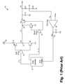
- buck-boost converters should be designed to prevent “chattering” between operations modes when the input and output voltages remain unchanged. Also, buck-boost converters should be designed to prevent transient jumping between operation modes. The problems that can occur during the transition between different operation modes in a conventional buck-boost converter are described with reference to FIG. 1 .
- FIG. 1 is a schematic diagram of a conventional buck-boost converter.
- a single inductor buck-boost converter 10 includes four power switches arranged in a bridge configuration.
- Power switches S 1 and S 2 form a first pair of switches and are referred to as the buck switches, while power switches S 3 and S 4 form a second pair of power switches and are referred to as the boost switches.
- Switch S 2 is sometimes referred to as a “buck recirculating switch” or “recirculating switch.”
- Power switches S 1 and S 2 are mutually exclusive in operation. That is, when switch S 1 is on, switch S 2 is off and vice versa.
- Power switches S 3 and S 4 are also mutually exclusive in operation. When switch S 3 is on, switch S 4 is off and vice versa.
- An output inductor L 1 is connected between the two pairs of power switches, that is, between nodes 22 and 24 .
- the switching of the power switches S 1 to S 4 causes a ramping current to flow in inductor L 1 .
- An output capacitor C 1 filters the ramping inductor current to generate a substantially constant output voltage Vout at an output node 26 .
- the proportion of time for which switch S 1 is closed is called the buck duty cycle
- the proportion of time for which switch S 3 is closed is called the boost duty cycle.
- the duty cycles for the buck and boost switch pairs are controlled independently to maintain a constant output voltage Vout for a given input voltage Vin.
- Regulation of the output voltage is realized through a voltage divider formed by resistors R 1 and R 2 which generates a stepped down output voltage as the feedback voltage V FB (node 29 ).
- the feedback voltage V FB is compared with a reference voltage V REF (node 30 ) at an error amplifier 20 .
- the error amplifier 20 generates an error voltage V ERR (node 32 ) indicative of the difference between the feedback voltage and the reference voltage.
- the error voltage V ERR is provided to a PWM controller 12 to generate the appropriate duty cycle for the buck power switches and the boost power switches.
- the PWM controller 12 generates buck drive signals for the buck driver 16 driving the buck switches S 1 , S 2 and generates boost drive signals for the boost driver 18 driving the boost switches S 3 , S 4 .
- the buck-boost converter 10 operates in the Buck mode when the input voltage is higher than the desired output voltage.
- switches S 1 and S 2 switches according to the Buck duty cycle while switch S 3 is open and switch S 4 is closed.
- switch S 1 is on for a longer and longer proportion of each cycle, and switch S 2 is on for less and less of each cycle. At some point, switch S 1 can no longer turn off fully at the end of each cycle and switch S 2 can no longer turn on fully. If no action was taken, the fixed frequency repetitive nature of the converter operation would be broken, and a series of pulses would ensue, where switch S 1 would be on for 100% of some cycles and less than 100% for others. This non-repetitive nature in the buck mode, at a time when the input voltage falls to a level approximately equals the output voltage, would cause the inductor current and output voltage ripple to undesirably increase if no remedial measure is taken.
- a Buck-Boost mode is an operation mode which is commonly used when the output voltage Vout is close to the input voltage Vin. In this mode, all four switches S 1 -S 4 operate as two independently controlled pairs of mutually exclusive switches. In the Buck-Boost mode, it is the relative time between switches S 3 and S 2 being on that causes the inductor current (and hence the output voltage) to increase or decrease over a whole cycle.
- the Boost mode In the Boost mode, switch S 1 is closed and switch S 2 is open. As the input voltage Vin falls below the fixed output voltage, switch S 3 is turned on for longer proportions of the switching period and hence switch S 4 comes on for shorter proportions of the switching period.
- the Boost mode In a similar way to the Buck mode, the Boost mode is limited by the minimum time for which switch S 3 can turn off. If the input to output voltage ratio then demands a longer on time for switch S 3 , then a repetitive fixed frequency operation would be broken and switch S 3 would be completely off for some periods and on for others, and the inductor current and output voltage ripple would undesirably increase.
- FIG. 2 illustrates the inductor current waveforms in the Buck Mode and the Buck-Boost Mode for the buck-boost converter of FIG. 1 .
- the buck-boost converter 10 Assuming the buck-boost converter 10 initially operate with an input voltage Vin much higher than the output voltage Vout, the buck-boost converter 10 is then operating in buck mode. Then, the input voltage Vin decreases while the converter attempts to maintain a constant output voltage Vout. In the Buck mode, the rate of increase of the inductor current in one cycle is related to the input voltage Vin minus the output voltage Vout, while the rate of decay of the inductor current is proportional to the output voltage Vout. For stable operation, the inductor current decays to the same level at the end of a cycle as the level at the start of the cycle, as shown by curve 40 in FIG. 2 .
- the slope of the rising segment of the inductor current is given as (Vin-Vout)/L, where L is the inductance of inductor L 1 .
- the slope of the decaying segment of the inductor current is given as Vout/L.
- the voltage across the inductor L 1 is related to a given combination of switches being turned on or closed. For instance, the voltage Vin across the inductor L 1 corresponds to switches S 1 and S 3 being on.
- the voltage Vin-Vout across the inductor L 1 corresponds to switches S 1 and S 4 being on.
- the voltage Vout across the inductor L 1 corresponds to switches S 2 and S 4 being on.
- This stable Buck mode operation (curve 40 ) reaches the mode transition limit when the turn off time of switch S 1 cannot be reduced any further. Then, if the input voltage Vin drops still further, the buck-boost converter 10 would want to go into the Buck-Boost mode.
- the transition into the Buck-Boost mode occurs when the input voltage Vin is slightly greater than the output voltage Vout because there is a small voltage drop in the converter.
- Curve 42 in FIG. 2 illustrates the inductor current waveform when the converter transitions into the Buck-Boost mode by introducing a minimum boost pulse at the start of each buck-boost cycle.
- the Buck mode At the start of the Buck-Boost mode, when the input voltage has fallen to slightly greater than the output voltage, the Buck mode continues to operate at its maximum duty cycle, so switch S 2 turns on for a minimum on-time at the end of each cycle. Also, at the start of the Buck-Boost mode, the boost switch S 3 turns on for the minimum on-time for the minimum boost duty cycle.
- the voltage control loop would cause the control signal in the converter to oscillate, choosing some buck cycles and some buck-boost cycles for switching, in order to try to make the output voltage Vout to be the desired regulated voltage. For instance, when the output voltage Vout becomes too high and the error voltage V ERR in the feedback loop reduces to a given level, the Buck mode would then be initiated in an attempt to lower the output voltage Vout to the desired level. Then, the Buck-Boost mode is initiated after the output voltage Vout falls too low. This oscillating behavior between two operation modes is undesirable but is seen on many of the converter devices commercially available today.
- the inductor current will fall more rapidly, but rise more slowly, at least during the Vin-Vout portion. Eventually the inductor current will be able to fall to the same level at which it started the cycle, and stable buck-boost operation is realized.
- Conventional buck-boost converters suffer many shortcomings, particularly in the chattering between operation modes and also in transient jumping between the operation modes.
- Conventional buck-boost converters are not able to realize smooth transitions into and out of the Buck-Boost mode.
- a DC-to-DC, buck-boost voltage converter including a first buck switching transistor coupled between an input voltage and a first terminal of an inductor, a second buck switching transistor coupled between the first terminal of the inductor and ground, a first boost switching transistor coupled between a second terminal of the inductor and ground, and a second boost switching transistor coupled between the second terminal of the inductor and an output terminal of the converter
- the converter includes a duty cycle controller configured to generate control signals for a buck driver configured to drive the first and second buck switching transistors at a buck duty cycle and to generate control signals for a boost driver configured to drive the first and second boost switching transistors at a boost duty cycle.
- the duty cycle controller includes at least a duty cycle timer and an offset timer where the duty cycle controller applies the duty cycle timer and the offset timer to control transitions between the buck, the buck-boost and the boost operation modes of the voltage converter.
- FIG. 1 is a schematic diagram of a conventional buck-boost converter.
- FIG. 2 illustrates the inductor current waveforms in the Buck Mode and the Buck-Boost Mode for the buck-boost converter of FIG. 1 .
- FIG. 3 is a schematic diagram of a buck-boost converter incorporating a duty cycle controller according to one embodiment of the present invention.
- FIG. 4 illustrates the inductor current waveforms in the Buck Mode and the Buck-Boost Mode for the buck-boost converter of FIG. 3 .
- FIG. 5 is a timing diagram illustrating the states of the power switches during different operation modes according to one embodiment of the present invention.
- FIG. 6 illustrates offset buck and boost ramping waveforms and the control voltage levels which can be used to control the switching of the power switches according to one embodiment of the present invention.
- FIG. 7 is a schematic diagram of a duty cycle controller which can be incorporated in the buck-boost converter of FIG. 3 according to one embodiment of the present invention.
- a buck-boost converter incorporates a duty cycle controller using timers to control the transition between Buck, Buck-Boost and Boost modes. More specifically, the timers in the duty cycle controller measure the duty cycle of the buck and boost power switches to determine the transition between the different operation modes.
- a duty cycle timer and an offset timer are used to establish the transition thresholds between the operation modes.
- hysteresis is implemented using the offset timer to prevent chattering or transient jumping between the operation modes.
- the duty cycle controller in the buck-boost converter of the present invention is configured to use timers to control the duty cycle.
- the duty cycle controller using timers is silicon area efficient and is also effective to minimize the buck-boost region when the converter is operated at different frequencies.
- the timers in the duty cycle controller of the present invention operate independently of the switching frequency so that the mode transition times are independent but synchronous of the switching frequency.
- the duty cycle controller with timers is able to achieve the smallest possible buck-boost operation time independent of the switching frequency to achieve optimal converter operation.
- the timers are generated from the main oscillator or the system clock of the electronic device in which the buck-boost converter is incorporated. Improved duty cycle accuracy is assured by using a copy of the oscillator current which is often trimmed for accuracy.
- the timers may be generated from a clock internal to the buck-boost converter where the clock may run faster than the maximum switching frequency.
- a phase-locked loop may be used to generate the high clock frequencies using a clock signal external or internal to the buck-boost converter.
- FIG. 3 is a schematic diagram of a buck-boost converter incorporating a duty cycle controller according to one embodiment of the present invention.
- a buck-boost converter 100 includes a duty cycle controller circuit 120 , power switches S 1 and S 2 for buck operation and power switches S 3 and S 4 for boost operation, an inductor L 1 , and an output capacitor C 1 .
- the buck-boost converter 100 receives an input voltage Vin on a node 28 and provides an output voltage Vout having a substantially constant magnitude on a node 26 for driving a load (not shown).
- a voltage divider circuit including resistors R 1 and R 2 divides down the output voltage Vout to provide a feedback voltage V FB (on node 29 ) to be fed back to the duty cycle controller circuit 120 to provide regulation and control of the output voltage.
- duty cycle controller circuit 120 may operate at a fixed switching frequency or a variable switching frequency.
- buck-boost converter 100 includes an error amplifier 20 for receiving the feedback voltage V FB and a reference voltage V REF and providing an error output voltage V ERR on a node 32 responsive to the difference between the feedback voltage and the reference voltage.
- a capacitor C 2 may be used at the output node of the error amplifier 20 to filter the error output voltage.
- the error output voltage V ERR is processed by the duty cycle controller circuit 120 to derive the control signals for driving the power switches in either the buck mode or the boost mode or the buck-boost mode of operation. Error output voltage V ERR is used to determine the duty cycle of the power switches in the buck mode, the buck-boost mode, and the boost mode of operation.
- duty cycle controller circuit 120 generates control signals for controlling a buck driver circuit 16 for driving the buck power switches S 1 and S 2 .
- Duty cycle controller circuit 120 also generates control signals for controlling a boost driver circuit 18 for driving the boost power switches S 3 and S 4 .
- buck switches S 1 and S 2 are connected in series between the input voltage Vin and the ground potential to drive a switching output voltage V SW on a switching output node 22 to which inductor L 1 is connected.
- Boost switches S 3 and S 4 are connected in series between the output voltage Vout and the ground potential to drive the other node 24 of the inductor L 1 .
- Duty cycle controller circuit 120 selects the buck, buck-boost or boost mode of operation depending on the input voltage Vin and the desired regulated output voltage Vout.
- the buck mode is selected and the boost switch S 4 is left on while the boost switch S 3 is left off.
- the buck switches S 1 and S 2 are then synchronously switched by the pulses from duty cycle controller circuit 120 at specific duty cycles to regulate the output voltage at the desired level.
- duty cycle controller circuit 120 drives the power switch S 1 to turn on so that inductor L 1 has the input voltage Vin impressed upon it and the current through the inductor builds up.
- the duty cycle controller circuit 120 turns off power switch S 1 and turns on power switch S 2 .
- the voltage across inductor L 1 reverses and inductor L 1 dumps energy through power switch S 4 onto output capacitor C 1 .
- the boost mode is selected and the buck S 1 is left on while the buck switch S 2 is left off.
- the boost switches S 3 and S 4 are then synchronously switched by the pulses from the duty cycle controller circuit 120 at specific duty cycles to regulate the output voltage at the desired level.
- the duty cycle controller circuit 120 turns on power switch S 3 to direct the inductor current to ground.
- the duty cycle controller circuit 120 drives the power switch S 4 to turn on and drives power switch S 3 to turn off so that the current from the input voltage Vin flows through the inductor L 1 and power switch S 4 to charge up output capacitor C 1 .
- the output voltage Vout is maintained by output capacitor C 1 until the next cycle when power switch S 3 is turned on again.
- the buck-boost mode is selected where the buck switches S 1 , S 2 and the boost switches S 3 and S 4 are synchronously switched by the pulses from the duty cycle controller circuit 120 at specific duty cycles to regulate the output voltage at the desired level. More specifically, in the buck-boost mode, the boost switch S 3 is turned on for at least the minimum on-time at the start of the duty cycle while buck switch S 1 is turned on. Then, at the end of the duty cycle, buck switch S 2 is turned on for the recirculation period.
- the buck-boost converter 100 of the present invention implements the mode transition methods descried in the aforementioned '602 patent application. More specifically, the mode transition methods described in the '602 patent application control the buck and boost duty cycles to ensure stable transitions into and out of the buck-boost mode. The mode transition methods of the '602 patent application will be described with reference to FIGS. 4-6 .
- FIG. 1 The mode transition methods of the '602 patent application will be described with reference to FIGS. 4-6 .
- FIG. 4 illustrates the inductor current waveforms in the Buck Mode and the Buck-Boost Mode for the buck-boost converter of FIG. 3 .
- FIG. 5 is a timing diagram illustrating the states of the power switches during different operation modes according to one embodiment of the present invention.
- FIG. 6 illustrates offset buck and boost ramping waveforms and the control voltage levels which can be used to control the switching of the power switches according to one embodiment of the present invention.
- FIG. 5 the on and off time of the power switches S 1 to S 4 with the input voltage Vin dropping is shown.
- the converter 100 is operated in the buck mode until the input voltage Vin drops to a level that is slightly higher than the output voltage Vout.
- the buck mode is operating at the maximum buck duty cycle where buck switch S 2 is on for the minimum on time and the buck duty cycle is less than 100%, such as between 90% to 95% (waveform set 50 in FIG. 5 ).
- the duty cycle controller 120 controls the buck and boost duty cycles of the converter 100 so that when the converter 100 enters the buck-boost mode (waveform set 52 in FIG. 5 ) from the buck mode, the boost duty cycle begins with a minimum boost switch on-time or minimum boost switch pulse width and the buck recirculation pulse is increased by the minimum on-time of the boost switch, thereby decreasing the buck duty cycle.
- boost switch S 3 is turned on at the beginning of the cycle for the minimum on-time or minimum pulse width and the buck recirculation switch S 2 , which is normally turned on at minimum pulse width, is now turned on for the minimum pulse width plus the minimum pulse width of the boost switch.
- the buck duty cycle the time which S 1 is turned on, is thus decreased to decrease the buck duty cycle.
- the input voltage is nominally the same as the output voltage.
- the increased buck recirculation pulse width causes the inductor current to fall by about the same amount as the rise in inductor current caused by the boost pulse. Therefore, the inductor current at the beginning of a switching cycle will be about the same as at the end of the switching cycle (curve 45 in FIG. 4 ), and stable transition operation is ensured.
- the boost switch S 3 increases its duty cycle so that it is on longer than the minimum on-time. Meanwhile, the buck switch S 2 on-time per cycle is reduced by the same amount so that the buck duty cycle is increased.
- the converter 100 From the buck-boost mode, the converter 100 enters the boost mode when the input voltage drops below the output voltage. At that point, the buck switch S 2 reaches the minimum pulse width (waveform set 54 in FIG. 5 ). Upon entering the boost mode, the buck recirculation pulse is stopped, that is, switch S 2 is kept open, and the on-time of the boost switch S 3 is immediately reduced by the same amount as the minimum on-time of the buck recirculation switch S 2 (waveform set 56 in FIG. 5 ). In this manner, the inductor current at the end of the cycle can return to the same current level that was at the start of a cycle. During the boost mode, buck switch S 1 is turned on while buck switch S 2 remains off.
- the duty cycle controller 120 operates the boost switches S 3 and S 4 to control the boost duty cycle.
- the buck-boost converter 100 can operate with no increased ripple or oscillation during the transitions into and out of the buck-boost mode.
- the duty cycle controller 120 applies a buck ramping waveform 60 and a boost ramping waveform 62 ( FIG. 6 ) to control the on-time of the power switches S 1 to S 4 .
- the error voltage V ERR (or other control voltage) is compared with the buck and boost ramping waveforms to determine the mode and the duty cycle of the converter.
- the duty cycle or the on-off times of the power switches may be compensated by applying offsets to the ramping waveforms or applying offsets to the error voltage or control voltage.
- the duty cycle controller 120 generates the control signals for driving the buck driver 16 and the boost driver 18 to control the duty cycles of the power switches S 1 to S 4 .
- control voltages 65 , 66 , 67 may be the error voltage V ERR in converter 100 or may be a demand signal in a current controlled loop.
- the level of the control voltages determines the operation mode of the converter and the duty cycles of the power switches S 1 -S 4 .
- the buck ramp waveform 60 and boost ramp waveform 62 are shown overlapping so that both the buck and boost switches are switched each cycle.
- the mode transition methods described herein apply to many different types of buck-boost converters using voltage control loops and/or current control loops.
- the control signal may represent an error voltage in a voltage loop or a current error in a current loop.
- the error voltage V ERR will cause the demand signal to be low in order to keep the feedback voltage V FB equal to V REF , and this will result in a lower overall average voltage demand across the inductor L 1 .
- An example of such a low demand signal is control voltage 65 , which only intersects the buck ramp waveform 60 during some portion of the cycle. Accordingly, the converter 100 will operate in the buck mode. In the buck mode, the boost switch S 4 will remain on, and the boost switch S 3 will remain off. From time T 0 to time Ta, the buck switch S 1 is on and switch S 2 is off. Between time Ta and T 1 , switch S 2 is on and switch S 1 is off. Accordingly, the buck ramp waveform 60 determines the buck duty cycle depending where on the ramp the control voltage intersects the waveform 60 .
- the error voltage V ERR When the input voltage Vin is significantly lower than the output voltage, the error voltage V ERR will cause a higher demand signal or control signal to be generated in order to keep the feedback voltage V FB equal to V REF .
- An example of such a high control signal is control voltage 66 , which only intersects the boost ramp waveform 62 during some portion of the cycle. Accordingly, the converter 100 will operate in the boost mode. In the boost mode, the buck switch S 1 will remain on, and the buck switch S 2 will remain off. From time T 0 to time Tb, the boost switch S 3 is on and switch S 4 is off. Between time Tb and T 1 , switch S 4 is on and switch S 3 is off. Accordingly, the boost ramp waveform 62 determines the boost duty cycle depending where on the ramp the control voltage intersects the waveform 62 .
- the duty cycles of the buck or boost switches will change to maintain the output voltage Vout at the regulated level. If the power supply is a battery, the control voltage increases as the battery voltage goes down, for a constant output voltage.
- the converter 100 When the input voltage Vin is slightly above the output voltage, the error voltage V ERR will cause a nominal demand signal or control signal to be generated in order to keep the feedback voltage V FB equal to V REF .
- An example of such a nominal control signal is control voltage 67 , which intersects the overlapping portion of the buck and boost ramp waveforms. Accordingly, the converter 100 will operate in the buck-boost mode.
- buck switch S 1 is closed and switch S 2 is open while boost switch S 4 is closed and switch S 3 is open.
- boost switch S 4 is closed and switch S 3 is open.
- buck switch S 1 is closed and switch S 2 is open while boost switch S 3 is closed and switch S 4 is open.
- the boost pulse is thus added to the beginning of the cycle. Accordingly, the buck ramp waveform 60 and the boost ramp waveform 62 determine the duty cycle depending where on the ramps the control voltage intersects the waveforms 60 , 62 .
- FIG. 7 is a schematic diagram of a duty cycle controller which can be incorporated in the buck-boost converter of FIG. 3 according to one embodiment of the present invention.
- the duty cycle controller 120 receives the buck and boost ramp waveforms 60 , 62 ( FIG. 6 ) and a control voltage Vc, which may be the error voltage V ERR or other control voltage, as input signals.
- the duty cycle controller 120 generate control signals for driving the buck and boost drivers 16 and 18 to control the duty cycle of the power switches S 1 to S 4 .
- Duty cycle controller 120 includes a buck PWM comparator 1 and a boost PWM comparator 2 which operate to compare the control voltage Vc to respective buck and boost ramp waveforms.
- the PWM comparators 1 and 2 generate a first set of control signals on nodes 70 , 72 indicative of the duty cycle for the buck switches (S 1 , S 2 ) and for the boost switches (S 3 , S 4 ).
- the buck-boost converter 100 uses timers to control the transition between the buck, buck-boost and boost operation modes.
- duty cycle controller 120 includes a duty cycle generation timer circuit 140 configured to measure the duty cycle of the buck and boost power switches and to control the transition between the operation modes.
- Duty cycle generation timer circuit 140 receives the first set of control signals from the PWM comparators 1 and 2 and generate a second set of control signals on nodes 74 , 76 for the buck driver 16 and the boost driver 18 .
- Duty cycle generation timer circuit 140 is operative to control the transition between operation modes only.
- the duty cycle generation time circuit 140 do not modify the duty cycle of the control signals and the first set of signals effectively passes through the timer circuit as the second set of signals for the buck and boost drivers.
- the duty cycle generation timer circuit 140 operates to detect the boundary conditions when the converter should transition to another mode of operation and the duty cycle generation timer circuit 140 determines the duty cycle or on-off time for the power switches to ensure a stable transition between operation modes.
- duty cycle generation timer circuit 140 implements two types of timer values or “timers”.
- a set of duty cycle timers also referred to as “D-timers,” is set to the minimum on/off time of the buck and boost power switches S 1 to S 4 .
- the duty cycle timers under worst case tolerance, meet the minimum on/off time specified for the power switches.
- the minimum on time and the minimum off time are assumed to be equal.
- a single duty cycle timer, or D-timer represents both the minimum on and the minimum off time for the power switches.
- a set of offset timers is used to specify a buffer time to accommodate for implementation tolerance in transistor switch time, such as variations over temperature, clock skew, or comparator offset.
- the offset timers are selected to accommodate the worst case skew over process and temperature of the duty cycle generation errors.
- a single offset timer, or O-timer is used for transitions to and from buck-boost modes.
- two or more offset timers may be used for different types of transitions, such as from buck-boost to buck mode or from buck-boost to boost mode.
- the duty cycle generation timer circuit 140 further implements hysteresis to prevent the buck-boost converter from chattering between operation modes.
- the hysteresis threshold is set as twice the offset timer. In other embodiments, the hysteresis threshold is set as N times the offset timer, N being a real number as N could be a division of the clock period.
- the duty cycle generation timer circuit 140 is implemented using a ring oscillator which can switch at a frequency faster than the switching frequency of the buck-boost converter. Furthermore, the ring oscillator may switch synchronously or asynchronously with the switching frequency of the buck-boost converter. In other embodiments, the duty cycle generation timer circuit 140 may be implemented using a phase-locked loop (PLL) where different timers can be generated as harmonics of the PLL.
- PLL phase-locked loop
- the duty cycle timers and offset timers are generated from the main oscillator or the system clock of the electronic device in which the buck-boost converter is incorporated.
- the system clock is synchronous with the switching frequency of the buck-boost converter. In other embodiments, the system clock may run at a frequency which is independent of the switching frequency of the buck-boost converter.
- the duty cycle timers and the offset timers are used for two purposes. First, the duty cycle timers and the offset timers are used for duty cycle generation, that is, to determine the duty cycle to use for the power switches during the mode transition. Second, the duty cycle timers and the offset timers are used for threshold control, that is, to determine when the transition thresholds are met to enter or exit between the different operation modes.
- the duty cycle generation timer circuit 140 digitally compares the buck and boost duty cycles to the transition threshold determined by the D-timers and the O-timers in order to determine the mode transition point. The duty cycle generation timer circuit 140 is thus able to perform near instant comparisons of the duty cycle versus the transition thresholds.
- the duty cycle controller implements a single duty cycle timer and a single offset timer.
- the duty cycle timer and the offset timer are used to specify the following transition thresholds:
- Buck to Buck-Boost threshold 1 ⁇ (D-timer * f s )
- Buck-Boost to Buck threshold 1 ⁇ ((D-timer + 2 * O-timer) * f s )
- Buck-Boost to Boost threshold 1 + ((2 * O-timer) * f s )
- f s denotes the switching frequency of the buck-boost converter from which the duty cycle timers and the offset timers are derived.
- different duty cycle timers and different offset timers may be used for the different transition thresholds.
- the O-timer used for the buck-boost to buck threshold may be different from the O-timer used for the buck-boost to boost threshold.
- the buck-boost converter 100 will transition from the buck mode to the buck-boost mode when the maximum buck duty cycle for the buck switch S 1 is reached, as given by threshold condition (1) above.
- the buck-boost converter 100 will transition back into the buck mode when the buck duty cycle (switch S 1 duty cycle) decreases below the maximum with hysteresis, as given by threshold condition (2) above.
- the buck-boost converter 100 will transition to the boost mode when the buck duty cycle plus the boost duty cycle exceeds 100% with hysteresis, as given by threshold condition (3) above.
- the buck-boost converter 100 when time for which switch S 1 is closed (buck duty cycle) to the time for which switch S 3 is closed in the next cycle (boost duty cycle) is greater than 100% with hysteresis, the buck-boost converter 100 will transition to the boost mode.
- the D-timer would have a value of 25 ns
- the O-timer would have a value of 5 ns (2%)
- the hysteresis would be 10 ns (4%).
- the switching frequency of the converter is also at 4 MHz (250 ns period).
- the buck-boost converter 100 will go from the buck mode to the buck-boost mode when the buck duty cycle reaches 90% (or 225 ns on time for switch S 1 ) being the maximum buck duty cycle.
- the minimum boost duty cycle is thus 10%.
- the duty cycle timer is buffered with hysteresis being two times the offset timer or 10 ns or 4% of the duty cycle.
- the buck duty cycle has to drop to 86% (or 215 ns on time for switch S 1 before the converter will be allowed to transition back into the buck mode.
- the buck duty cycle plus the boost duty cycle exceeds the 100% duty cycle by the hysteresis (4%).
- a salient feature of the duty cycle controller 120 of the present invention is that when the switching frequency is reduced, then the percentage duty cycle (and hence the operating range) for which the buck-boost mode operates reduces accordingly.
- Table 1 below illustrates one exemplary embodiment of buck and boost duty cycle values for increasing control voltage at the mode transition boundary from the buck mode to the buck-boost mode.
- the control voltage is indicative of the error voltage generated by the error amplifier comparing the feedback voltage of the buck-boost converter to a reference voltage.
- the above-described conditions for the buck-boost converter apply. That is, the switching frequency is 4 MHz, the maximum buck duty cycle is 90%, the minimum boost duty cycle is 10%, the offset timer is 5 ns or 2% and the hysteresis is 10 ns and 4%.
- the duty cycle controller of the present invention uses the duty cycle timers and the offset timers to determine the duty cycle at the transition point and also the threshold for making the transition.
- the buck-boost converter With the input voltage Vin greater than the output voltage, the buck-boost converter is operated in the buck mode. As the control voltage increases, the buck duty cycle increases until the maximum buck duty cycle of 90% is reached with the boost duty cycle at 0%. When the buck duty cycle reaches the transition threshold of 90% as measured by the duty cycle generation timer circuit, the buck-boost converter is about to enter the buck-boost mode. At this time, the recirculation pulse is at a minimum pulse width of 25ns or 10% duty cycle. At the transition point, the boost duty cycle is increased from 0% to 14% which is the 10% minimum duty cycle plus 4% hysteresis.
- a 16% recirculation pulse is added which increases the recirculation pulse to 26% and decreases the buck duty cycle to 74%.
- the recirculation pulse is increased by 2% more than the increase in the boost duty cycle.
- the additional 2% offset added to the recirculation pulse represents “overcooking” of the compensation to ensure stability in the transition.
- the boost duty cycle and the buck duty cycle both increase from the value at the transition point.
- Table 2 illustrates one exemplary embodiment of buck and boost duty cycle values for increasing control voltage at the mode transition boundary from the buck-boost mode to the boost mode.
- the above-described conditions for the buck-boost converter apply.
- the buck-boost converter transitions to the boost mode.
- the buck duty cycle reaches 88% and the recirculation duty cycle at 12% which is the minimum duty cycle plus the 2% offset and the boost pulse is at 28% duty cycle, the converter is about to leave the buck-boost mode and enter the boost mode.
- the buck duty cycle is increased by 12% to 100% which eliminated the recirculation pulse.
- the boost duty cycle is decreased by 14% down to 14%.
- the boost duty cycle is decreased 2% more than the increase in the buck duty cycle (or the removal of the recirculation pulse) to realize a 2% offset.
- the additional 2% offset reduction in the boost pulse represents “overcooking” of the compensation to ensure stability in the transition.
- hysteresis is applied to prevent chattering between operation modes.
- the buck-boost converter is operated in the boost mode and the input voltage increases, the buck-boost converter is to transition to the buck-boost mode.
- the buck duty cycle is 100% (no recirculation pulse) while the boost duty cycle is at 10%, the minimum duty cycle.
- the buck duty cycle is decreased by 12% to 88% in order to add the recirculation pulse while the boost duty cycle is increased by 14% to 24%.
- the boost duty cycle is increased by 2% offset more than the reduction in the buck duty cycle to ensure stability.
- the buck-boost converter is to transition to the buck mode.
- the buck duty cycle is 74% (26% recirculation pulse) while the boost duty cycle is at 10%, the minimum duty cycle.
- the buck duty cycle is increased by 12% to 86% while the boost duty cycle is decreased by 10% to 0%.
- the buck duty cycle is increased by 2% offset more than the reduction in the boost duty cycle to ensure stability.
Landscapes
- Engineering & Computer Science (AREA)
- Power Engineering (AREA)
- Dc-Dc Converters (AREA)
Abstract
Description
| (1) | Buck to Buck-Boost threshold: | 1 − (D-timer * fs) |
| (2) | Buck-Boost to Buck threshold: | 1 − ((D- |
| (3) | Buck-Boost to Boost threshold: | 1 + ((2 * O-timer) * fs) |
where fs denotes the switching frequency of the buck-boost converter from which the duty cycle timers and the offset timers are derived. In other embodiments, different duty cycle timers and different offset timers may be used for the different transition thresholds. For example, the O-timer used for the buck-boost to buck threshold may be different from the O-timer used for the buck-boost to boost threshold.
| Control Voltage | ||
| 0.43 V+ | 0.45 V | 0.45 V+ | 0.5 V | ||
| Buck Duty Cycle | 86% | 90% | 74% | 84% |
| (−16%) | ||||
| Boost Duty Cycle | 0% | 0% | 14% | 24% |
| (+14%) | ||||
| Operation Mode | Buck | Buck | Buck-Boost | Buck-Boost |
| Control Voltage | ||
| 0.5 V+ | 0.52 V | 0.52 V+ | 0.875 V | ||
| Buck Duty Cycle | 84% | 88% | 100% | 100% |
| (+12%) | ||||
| |
24% | 28% | 14% | 75% |
| (−14%) | ||||
| Operation Mode | Buck-Boost | Buck-Boost | Boost | Boost |
Claims (14)
Priority Applications (1)
| Application Number | Priority Date | Filing Date | Title |
|---|---|---|---|
| US13/277,559 US8773084B2 (en) | 2009-08-24 | 2011-10-20 | Buck-boost converter using timers for mode transition control |
Applications Claiming Priority (2)
| Application Number | Priority Date | Filing Date | Title |
|---|---|---|---|
| US12/546,602 US8436591B2 (en) | 2009-08-24 | 2009-08-24 | Buck-boost converter with smooth transitions between modes |
| US13/277,559 US8773084B2 (en) | 2009-08-24 | 2011-10-20 | Buck-boost converter using timers for mode transition control |
Related Parent Applications (1)
| Application Number | Title | Priority Date | Filing Date |
|---|---|---|---|
| US12/546,602 Continuation-In-Part US8436591B2 (en) | 2009-08-24 | 2009-08-24 | Buck-boost converter with smooth transitions between modes |
Publications (2)
| Publication Number | Publication Date |
|---|---|
| US20120032658A1 US20120032658A1 (en) | 2012-02-09 |
| US8773084B2 true US8773084B2 (en) | 2014-07-08 |
Family
ID=45555685
Family Applications (1)
| Application Number | Title | Priority Date | Filing Date |
|---|---|---|---|
| US13/277,559 Active 2029-10-16 US8773084B2 (en) | 2009-08-24 | 2011-10-20 | Buck-boost converter using timers for mode transition control |
Country Status (1)
| Country | Link |
|---|---|
| US (1) | US8773084B2 (en) |
Cited By (15)
| Publication number | Priority date | Publication date | Assignee | Title |
|---|---|---|---|---|
| US20120319667A1 (en) * | 2010-02-12 | 2012-12-20 | Nxp B.V. | Dc-dc converter arrangement |
| US20140092641A1 (en) * | 2012-10-03 | 2014-04-03 | Inno-Tech Co., Ltd. | Synchronous rectifying buck-boost converter |
| US20140197814A1 (en) * | 2013-01-11 | 2014-07-17 | Qualcomm Incorporated | Programmable frequency range for boost converter clocks |
| US20140232360A1 (en) * | 2013-02-19 | 2014-08-21 | Nvidia Corporation | Predictive current sensing |
| US20160078842A1 (en) * | 2014-09-11 | 2016-03-17 | Pixtronix, Inc. | Universal digital controller design for dc/dc switching power supplies used in displays |
| US20160365790A1 (en) * | 2015-06-15 | 2016-12-15 | Futurewei Technologies, Inc. | Control Method for Buck-Boost Power Converters |
| US9647546B2 (en) | 2013-12-05 | 2017-05-09 | Fairchild Semiconductor Corporation | Dual-mode voltage doubling buck converter with smooth mode transition |
| US9800158B2 (en) | 2013-01-30 | 2017-10-24 | Nvidia Corporation | Current-parking switching regulator downstream controller |
| US9804621B2 (en) | 2013-02-05 | 2017-10-31 | Nvidia Corporation | Current-parking switching regulator downstream controller pre-driver |
| US10389250B1 (en) * | 2018-04-17 | 2019-08-20 | Aura Semiconductor Pvt. Ltd | Operating mode for a DC-DC converter to obtain a broad range of output voltages |
| WO2019191376A1 (en) * | 2018-03-30 | 2019-10-03 | Texas Instruments Incorporated | Timer for creating a stable on time |
| US10594218B1 (en) | 2017-12-20 | 2020-03-17 | Renesas Electronics America Inc. | Hysteresis timing scheme for mode transition in a buck boost converter |
| US10637357B1 (en) | 2017-12-20 | 2020-04-28 | Renesas Electronics America Inc. | Ramp offset compensation circuit in a buck boost converter |
| TWI779997B (en) * | 2021-12-21 | 2022-10-01 | 立錡科技股份有限公司 | Constant time buck-boost switching converter and modulation control circuit and control method thereof |
| US11695340B2 (en) | 2020-09-28 | 2023-07-04 | Samsung Electronics Co., Ltd. | Electronic device performing direct voltage to direct voltage conversion converting an input voltage to a fixed output voltage and operating method of electronic device |
Families Citing this family (46)
| Publication number | Priority date | Publication date | Assignee | Title |
|---|---|---|---|---|
| US9467053B2 (en) * | 2009-07-09 | 2016-10-11 | Infineon Technologies Ag | Controlling a multi-mode switching converter |
| US8446133B2 (en) * | 2010-01-08 | 2013-05-21 | Mediatek Inc. | Methods and control circuits for controlling buck-boost converting circuit to generate regulated output voltage under reduced average inductor current |
| US9099961B2 (en) | 2010-04-19 | 2015-08-04 | Rf Micro Devices, Inc. | Output impedance compensation of a pseudo-envelope follower power management system |
| US9431974B2 (en) | 2010-04-19 | 2016-08-30 | Qorvo Us, Inc. | Pseudo-envelope following feedback delay compensation |
| EP2782247B1 (en) | 2010-04-19 | 2018-08-15 | Qorvo US, Inc. | Pseudo-envelope following power management system |
| US9954436B2 (en) | 2010-09-29 | 2018-04-24 | Qorvo Us, Inc. | Single μC-buckboost converter with multiple regulated supply outputs |
| US9379667B2 (en) | 2011-05-05 | 2016-06-28 | Rf Micro Devices, Inc. | Multiple power supply input parallel amplifier based envelope tracking |
| US9484797B2 (en) | 2011-10-26 | 2016-11-01 | Qorvo Us, Inc. | RF switching converter with ripple correction |
| US9515621B2 (en) | 2011-11-30 | 2016-12-06 | Qorvo Us, Inc. | Multimode RF amplifier system |
| US9041365B2 (en) | 2011-12-01 | 2015-05-26 | Rf Micro Devices, Inc. | Multiple mode RF power converter |
| US9494962B2 (en) | 2011-12-02 | 2016-11-15 | Rf Micro Devices, Inc. | Phase reconfigurable switching power supply |
| US9813036B2 (en) | 2011-12-16 | 2017-11-07 | Qorvo Us, Inc. | Dynamic loadline power amplifier with baseband linearization |
| FR2991835B1 (en) * | 2012-06-08 | 2015-07-17 | Faurecia Sieges Automobile | CONTROL CIRCUIT FOR A PIEZOELECTRIC ENGINE POWERED BY THE BATTERY OF A MOTOR VEHICLE |
| KR101928020B1 (en) * | 2012-07-17 | 2019-03-13 | 삼성디스플레이 주식회사 | Voltage Generator and Organic Light Emitting Display Device Using the same |
| KR20140013706A (en) * | 2012-07-26 | 2014-02-05 | 삼성디스플레이 주식회사 | Driving method of voltage generator and organic light emitting display device using the same |
| US9698684B2 (en) * | 2012-08-27 | 2017-07-04 | Bombardier Transportation Gmbh | Adaptive soft switching control for power converter |
| US9627975B2 (en) * | 2012-11-16 | 2017-04-18 | Qorvo Us, Inc. | Modulated power supply system and method with automatic transition between buck and boost modes |
| US9929696B2 (en) | 2013-01-24 | 2018-03-27 | Qorvo Us, Inc. | Communications based adjustments of an offset capacitive voltage |
| US9124231B2 (en) | 2013-01-28 | 2015-09-01 | Qualcomm, Inc. | Soft turn-off for boost converters |
| EP2779398B1 (en) * | 2013-03-15 | 2019-01-23 | Dialog Semiconductor GmbH | A control method of high efficient buck-boost switching regulator |
| US9479118B2 (en) | 2013-04-16 | 2016-10-25 | Rf Micro Devices, Inc. | Dual instantaneous envelope tracking |
| US9231476B2 (en) * | 2013-05-01 | 2016-01-05 | Texas Instruments Incorporated | Tracking energy consumption using a boost-buck technique |
| DE102013105264A1 (en) * | 2013-05-23 | 2014-11-27 | Hella Kgaa Hueck & Co. | Control device for a DC-DC converter |
| CN104300927B (en) * | 2013-07-16 | 2019-04-16 | 马维尔国际贸易有限公司 | Adaptive boosting power supply with gradient control |
| US9923528B2 (en) * | 2013-07-16 | 2018-03-20 | Marvell World Trade Ltd. | Adaptive boost supply with slope control |
| US9374005B2 (en) | 2013-08-13 | 2016-06-21 | Rf Micro Devices, Inc. | Expanded range DC-DC converter |
| US9614476B2 (en) | 2014-07-01 | 2017-04-04 | Qorvo Us, Inc. | Group delay calibration of RF envelope tracking |
| US9614380B2 (en) * | 2014-10-10 | 2017-04-04 | Intersil Americas LLC | Hysteretic current mode buck-boost control architecture |
| US9843294B2 (en) | 2015-07-01 | 2017-12-12 | Qorvo Us, Inc. | Dual-mode envelope tracking power converter circuitry |
| US9912297B2 (en) | 2015-07-01 | 2018-03-06 | Qorvo Us, Inc. | Envelope tracking power converter circuitry |
| US9882488B2 (en) * | 2015-09-14 | 2018-01-30 | Intersil Americas LLC | Enhanced power mode transitions in buck-boost converters |
| DE102015223768B4 (en) * | 2015-11-30 | 2019-10-31 | Dialog Semiconductor (Uk) Limited | Buck-boost converter |
| JP6594199B2 (en) * | 2015-12-28 | 2019-10-23 | ローム株式会社 | Switching regulator |
| KR102592901B1 (en) * | 2016-02-26 | 2023-10-24 | 삼성디스플레이 주식회사 | Dc-dc converter, method of dc-dc converting using the same and display apparatus having the same |
| US9973147B2 (en) | 2016-05-10 | 2018-05-15 | Qorvo Us, Inc. | Envelope tracking power management circuit |
| US10128757B2 (en) * | 2017-03-03 | 2018-11-13 | Dialog Semiconductor (Uk) Limited | Buck-boost converter with small disturbance at mode transitions |
| US10931198B2 (en) * | 2017-12-08 | 2021-02-23 | Texas Instruments Incorporated | Buck-boost power converter controller |
| US10476437B2 (en) | 2018-03-15 | 2019-11-12 | Qorvo Us, Inc. | Multimode voltage tracker circuit |
| US11183935B2 (en) * | 2019-03-14 | 2021-11-23 | Microchip Technology Incorporated | Current control for buck-boost converters using conditional offsets |
| US11070129B2 (en) * | 2019-04-05 | 2021-07-20 | Oregon State University | Ultra low-voltage circuits |
| IT201900014715A1 (en) * | 2019-08-13 | 2021-02-13 | St Microelectronics Srl | CONTROL DEVICE FOR SWITCHING VOLTAGE REGULATOR AND CONTROL METHOD |
| US10790747B1 (en) | 2019-10-07 | 2020-09-29 | Analog Devices International Unlimited Company | Inductor current shunt for mitigation of load dump transients in DC-DC regulators |
| CN110635689A (en) * | 2019-10-22 | 2019-12-31 | 四川甘华电源科技有限公司 | Airborne miniaturized power failure holding module and working method thereof |
| US11811324B2 (en) | 2020-08-07 | 2023-11-07 | Monolithic Power Systems, Inc. | Integrated circuit of a buck-boost converter with output current sensing function |
| US11329563B2 (en) * | 2020-08-07 | 2022-05-10 | Chengdu Monolithic Power Systems Co., Ltd. | Buck-boost converter circuit, control circuit and associated control method |
| US11552555B2 (en) * | 2020-12-31 | 2023-01-10 | Texas Instruments Incorporated | Circuit electromagnetic interference control |
Citations (4)
| Publication number | Priority date | Publication date | Assignee | Title |
|---|---|---|---|---|
| US7432689B2 (en) * | 2006-05-05 | 2008-10-07 | Micrel, Inc. | Buck-boost control logic for PWM regulator |
| US20090045786A1 (en) | 2007-08-14 | 2009-02-19 | Freescale Semiconductor, Inc. | Mode transitioning in a dc/dc converter using a constant duty cycle difference |
| US20100244801A1 (en) * | 2009-03-27 | 2010-09-30 | Diodes Zetex Semiconductors Limited | Controller for switching regulator, switching regulator and light source |
| US20110043172A1 (en) * | 2009-08-24 | 2011-02-24 | Micrel, Inc. | Buck-Boost Converter With Smooth Transitions Between Modes |
-
2011
- 2011-10-20 US US13/277,559 patent/US8773084B2/en active Active
Patent Citations (4)
| Publication number | Priority date | Publication date | Assignee | Title |
|---|---|---|---|---|
| US7432689B2 (en) * | 2006-05-05 | 2008-10-07 | Micrel, Inc. | Buck-boost control logic for PWM regulator |
| US20090045786A1 (en) | 2007-08-14 | 2009-02-19 | Freescale Semiconductor, Inc. | Mode transitioning in a dc/dc converter using a constant duty cycle difference |
| US20100244801A1 (en) * | 2009-03-27 | 2010-09-30 | Diodes Zetex Semiconductors Limited | Controller for switching regulator, switching regulator and light source |
| US20110043172A1 (en) * | 2009-08-24 | 2011-02-24 | Micrel, Inc. | Buck-Boost Converter With Smooth Transitions Between Modes |
Cited By (22)
| Publication number | Priority date | Publication date | Assignee | Title |
|---|---|---|---|---|
| US20120319667A1 (en) * | 2010-02-12 | 2012-12-20 | Nxp B.V. | Dc-dc converter arrangement |
| US8866454B2 (en) * | 2010-02-12 | 2014-10-21 | Nxp B.V. | DC-DC converter arrangement |
| US20140092641A1 (en) * | 2012-10-03 | 2014-04-03 | Inno-Tech Co., Ltd. | Synchronous rectifying buck-boost converter |
| US8988051B2 (en) * | 2012-10-03 | 2015-03-24 | Inno-Tech Co., Ltd. | Synchronous rectifying buck-boost converter |
| US20140197814A1 (en) * | 2013-01-11 | 2014-07-17 | Qualcomm Incorporated | Programmable frequency range for boost converter clocks |
| US9372492B2 (en) * | 2013-01-11 | 2016-06-21 | Qualcomm Incorporated | Programmable frequency range for boost converter clocks |
| US9800158B2 (en) | 2013-01-30 | 2017-10-24 | Nvidia Corporation | Current-parking switching regulator downstream controller |
| US9804621B2 (en) | 2013-02-05 | 2017-10-31 | Nvidia Corporation | Current-parking switching regulator downstream controller pre-driver |
| US20140232360A1 (en) * | 2013-02-19 | 2014-08-21 | Nvidia Corporation | Predictive current sensing |
| US9639102B2 (en) * | 2013-02-19 | 2017-05-02 | Nvidia Corporation | Predictive current sensing |
| US9647546B2 (en) | 2013-12-05 | 2017-05-09 | Fairchild Semiconductor Corporation | Dual-mode voltage doubling buck converter with smooth mode transition |
| US20160078842A1 (en) * | 2014-09-11 | 2016-03-17 | Pixtronix, Inc. | Universal digital controller design for dc/dc switching power supplies used in displays |
| US20160365790A1 (en) * | 2015-06-15 | 2016-12-15 | Futurewei Technologies, Inc. | Control Method for Buck-Boost Power Converters |
| US10177661B2 (en) * | 2015-06-15 | 2019-01-08 | Futurewei Technologies, Inc. | Control method for buck-boost power converters |
| US10554130B2 (en) | 2015-06-15 | 2020-02-04 | Futurewei Technologies, Inc. | Control method for buck-boost power converters |
| US10594218B1 (en) | 2017-12-20 | 2020-03-17 | Renesas Electronics America Inc. | Hysteresis timing scheme for mode transition in a buck boost converter |
| US10637357B1 (en) | 2017-12-20 | 2020-04-28 | Renesas Electronics America Inc. | Ramp offset compensation circuit in a buck boost converter |
| WO2019191376A1 (en) * | 2018-03-30 | 2019-10-03 | Texas Instruments Incorporated | Timer for creating a stable on time |
| US10523116B2 (en) | 2018-03-30 | 2019-12-31 | Texas Instruments Incorporated | Timer for creating a stable on time |
| US10389250B1 (en) * | 2018-04-17 | 2019-08-20 | Aura Semiconductor Pvt. Ltd | Operating mode for a DC-DC converter to obtain a broad range of output voltages |
| US11695340B2 (en) | 2020-09-28 | 2023-07-04 | Samsung Electronics Co., Ltd. | Electronic device performing direct voltage to direct voltage conversion converting an input voltage to a fixed output voltage and operating method of electronic device |
| TWI779997B (en) * | 2021-12-21 | 2022-10-01 | 立錡科技股份有限公司 | Constant time buck-boost switching converter and modulation control circuit and control method thereof |
Also Published As
| Publication number | Publication date |
|---|---|
| US20120032658A1 (en) | 2012-02-09 |
Similar Documents
| Publication | Publication Date | Title |
|---|---|---|
| US8773084B2 (en) | Buck-boost converter using timers for mode transition control | |
| US8436591B2 (en) | Buck-boost converter with smooth transitions between modes | |
| US8593125B1 (en) | Buck DC-DC converter with dual feedback control | |
| US7443148B2 (en) | Constant on-time regulator with increased maximum duty cycle | |
| US20220052675A1 (en) | Current Mode Control Modulator Including Ramp Signal Generator Providing Slope Compensation | |
| US7382114B2 (en) | PFM-PWM DC-DC converter providing DC offset correction to PWM error amplifier and equalizing regulated voltage conditions when transitioning between PFM and PWM modes | |
| US7443150B2 (en) | Switching power supply control with phase shift | |
| US7482791B2 (en) | Constant on-time regulator with internal ripple generation and improved output voltage accuracy | |
| JP6175147B2 (en) | Soft start circuit and technique | |
| US7148670B2 (en) | Dual mode buck regulator with improved transition between LDO and PWM operation | |
| US8319487B2 (en) | Non-isolated current-mode-controlled switching voltage regulator | |
| JP3981110B2 (en) | Multi-phase synthesis ripple voltage regulator synchronization | |
| US7863875B1 (en) | Non-linear control techniques for improving transient response to load current step change | |
| US7723967B2 (en) | Step-up converter having an improved dynamic response | |
| US7498786B2 (en) | Digital control of switching voltage regulators | |
| US7489121B2 (en) | Compensation offset adjustment scheme for fast reference voltage transitioning | |
| US7619395B2 (en) | End-point prediction scheme for voltage regulators | |
| US7839667B2 (en) | Adaptive leading-edge blanking circuit and method for switching mode power converter | |
| US20090153124A1 (en) | Dc-to-dc converter | |
| US11394291B2 (en) | Ripple voltage control circuit and control method thereof | |
| JP2003525013A (en) | Power converter mode conversion method and device | |
| TW201929401A (en) | Constant on-time switching regulator for zero ESR output capacitor without output voltage offset and control circuit and method thereof | |
| US11223273B2 (en) | Sub-harmonic oscillation control in peak current limit mode switching system | |
| US20080030183A1 (en) | Method of feedback controlling a switched regulator | |
| CN115437440B (en) | Voltage regulator and compensation method thereof |
Legal Events
| Date | Code | Title | Description |
|---|---|---|---|
| AS | Assignment |
Owner name: MICREL, INC., CALIFORNIA Free format text: ASSIGNMENT OF ASSIGNORS INTEREST;ASSIGNORS:CASEY, CHARLES A.;DEARN, DAVID;SIGNING DATES FROM 20111019 TO 20111020;REEL/FRAME:027123/0909 |
|
| STCF | Information on status: patent grant |
Free format text: PATENTED CASE |
|
| MAFP | Maintenance fee payment |
Free format text: PAYMENT OF MAINTENANCE FEE, 4TH YEAR, LARGE ENTITY (ORIGINAL EVENT CODE: M1551) Year of fee payment: 4 |
|
| AS | Assignment |
Owner name: JPMORGAN CHASE BANK, N.A., AS ADMINISTRATIVE AGENT, DELAWARE Free format text: SECURITY INTEREST;ASSIGNORS:MICROCHIP TECHNOLOGY INC.;SILICON STORAGE TECHNOLOGY, INC.;ATMEL CORPORATION;AND OTHERS;REEL/FRAME:053311/0305 Effective date: 20200327 |
|
| AS | Assignment |
Owner name: MICROSEMI CORPORATION, CALIFORNIA Free format text: RELEASE BY SECURED PARTY;ASSIGNOR:JPMORGAN CHASE BANK, N.A, AS ADMINISTRATIVE AGENT;REEL/FRAME:053466/0011 Effective date: 20200529 Owner name: ATMEL CORPORATION, ARIZONA Free format text: RELEASE BY SECURED PARTY;ASSIGNOR:JPMORGAN CHASE BANK, N.A, AS ADMINISTRATIVE AGENT;REEL/FRAME:053466/0011 Effective date: 20200529 Owner name: MICROCHIP TECHNOLOGY INC., ARIZONA Free format text: RELEASE BY SECURED PARTY;ASSIGNOR:JPMORGAN CHASE BANK, N.A, AS ADMINISTRATIVE AGENT;REEL/FRAME:053466/0011 Effective date: 20200529 Owner name: MICROSEMI STORAGE SOLUTIONS, INC., ARIZONA Free format text: RELEASE BY SECURED PARTY;ASSIGNOR:JPMORGAN CHASE BANK, N.A, AS ADMINISTRATIVE AGENT;REEL/FRAME:053466/0011 Effective date: 20200529 Owner name: SILICON STORAGE TECHNOLOGY, INC., ARIZONA Free format text: RELEASE BY SECURED PARTY;ASSIGNOR:JPMORGAN CHASE BANK, N.A, AS ADMINISTRATIVE AGENT;REEL/FRAME:053466/0011 Effective date: 20200529 |
|
| AS | Assignment |
Owner name: WELLS FARGO BANK, NATIONAL ASSOCIATION, MINNESOTA Free format text: SECURITY INTEREST;ASSIGNORS:MICROCHIP TECHNOLOGY INC.;SILICON STORAGE TECHNOLOGY, INC.;ATMEL CORPORATION;AND OTHERS;REEL/FRAME:053468/0705 Effective date: 20200529 |
|
| AS | Assignment |
Owner name: WELLS FARGO BANK, NATIONAL ASSOCIATION, AS COLLATERAL AGENT, MINNESOTA Free format text: SECURITY INTEREST;ASSIGNORS:MICROCHIP TECHNOLOGY INCORPORATED;SILICON STORAGE TECHNOLOGY, INC.;ATMEL CORPORATION;AND OTHERS;REEL/FRAME:055671/0612 Effective date: 20201217 |
|
| AS | Assignment |
Owner name: WELLS FARGO BANK, NATIONAL ASSOCIATION, AS NOTES COLLATERAL AGENT, MINNESOTA Free format text: SECURITY INTEREST;ASSIGNORS:MICROCHIP TECHNOLOGY INCORPORATED;SILICON STORAGE TECHNOLOGY, INC.;ATMEL CORPORATION;AND OTHERS;REEL/FRAME:057935/0474 Effective date: 20210528 |
|
| MAFP | Maintenance fee payment |
Free format text: PAYMENT OF MAINTENANCE FEE, 8TH YEAR, LARGE ENTITY (ORIGINAL EVENT CODE: M1552); ENTITY STATUS OF PATENT OWNER: LARGE ENTITY Year of fee payment: 8 |
|
| AS | Assignment |
Owner name: MICROSEMI STORAGE SOLUTIONS, INC., ARIZONA Free format text: RELEASE BY SECURED PARTY;ASSIGNOR:WELLS FARGO BANK, NATIONAL ASSOCIATION, AS NOTES COLLATERAL AGENT;REEL/FRAME:059863/0400 Effective date: 20220228 Owner name: MICROSEMI CORPORATION, ARIZONA Free format text: RELEASE BY SECURED PARTY;ASSIGNOR:WELLS FARGO BANK, NATIONAL ASSOCIATION, AS NOTES COLLATERAL AGENT;REEL/FRAME:059863/0400 Effective date: 20220228 Owner name: ATMEL CORPORATION, ARIZONA Free format text: RELEASE BY SECURED PARTY;ASSIGNOR:WELLS FARGO BANK, NATIONAL ASSOCIATION, AS NOTES COLLATERAL AGENT;REEL/FRAME:059863/0400 Effective date: 20220228 Owner name: SILICON STORAGE TECHNOLOGY, INC., ARIZONA Free format text: RELEASE BY SECURED PARTY;ASSIGNOR:WELLS FARGO BANK, NATIONAL ASSOCIATION, AS NOTES COLLATERAL AGENT;REEL/FRAME:059863/0400 Effective date: 20220228 Owner name: MICROCHIP TECHNOLOGY INCORPORATED, ARIZONA Free format text: RELEASE BY SECURED PARTY;ASSIGNOR:WELLS FARGO BANK, NATIONAL ASSOCIATION, AS NOTES COLLATERAL AGENT;REEL/FRAME:059863/0400 Effective date: 20220228 |
|
| AS | Assignment |
Owner name: MICROSEMI STORAGE SOLUTIONS, INC., ARIZONA Free format text: RELEASE BY SECURED PARTY;ASSIGNOR:WELLS FARGO BANK, NATIONAL ASSOCIATION, AS NOTES COLLATERAL AGENT;REEL/FRAME:059363/0001 Effective date: 20220228 Owner name: MICROSEMI CORPORATION, ARIZONA Free format text: RELEASE BY SECURED PARTY;ASSIGNOR:WELLS FARGO BANK, NATIONAL ASSOCIATION, AS NOTES COLLATERAL AGENT;REEL/FRAME:059363/0001 Effective date: 20220228 Owner name: ATMEL CORPORATION, ARIZONA Free format text: RELEASE BY SECURED PARTY;ASSIGNOR:WELLS FARGO BANK, NATIONAL ASSOCIATION, AS NOTES COLLATERAL AGENT;REEL/FRAME:059363/0001 Effective date: 20220228 Owner name: SILICON STORAGE TECHNOLOGY, INC., ARIZONA Free format text: RELEASE BY SECURED PARTY;ASSIGNOR:WELLS FARGO BANK, NATIONAL ASSOCIATION, AS NOTES COLLATERAL AGENT;REEL/FRAME:059363/0001 Effective date: 20220228 Owner name: MICROCHIP TECHNOLOGY INCORPORATED, ARIZONA Free format text: RELEASE BY SECURED PARTY;ASSIGNOR:WELLS FARGO BANK, NATIONAL ASSOCIATION, AS NOTES COLLATERAL AGENT;REEL/FRAME:059363/0001 Effective date: 20220228 |
|
| AS | Assignment |
Owner name: MICROSEMI STORAGE SOLUTIONS, INC., ARIZONA Free format text: RELEASE BY SECURED PARTY;ASSIGNOR:WELLS FARGO BANK, NATIONAL ASSOCIATION, AS NOTES COLLATERAL AGENT;REEL/FRAME:060894/0437 Effective date: 20220228 Owner name: MICROSEMI CORPORATION, ARIZONA Free format text: RELEASE BY SECURED PARTY;ASSIGNOR:WELLS FARGO BANK, NATIONAL ASSOCIATION, AS NOTES COLLATERAL AGENT;REEL/FRAME:060894/0437 Effective date: 20220228 Owner name: ATMEL CORPORATION, ARIZONA Free format text: RELEASE BY SECURED PARTY;ASSIGNOR:WELLS FARGO BANK, NATIONAL ASSOCIATION, AS NOTES COLLATERAL AGENT;REEL/FRAME:060894/0437 Effective date: 20220228 Owner name: SILICON STORAGE TECHNOLOGY, INC., ARIZONA Free format text: RELEASE BY SECURED PARTY;ASSIGNOR:WELLS FARGO BANK, NATIONAL ASSOCIATION, AS NOTES COLLATERAL AGENT;REEL/FRAME:060894/0437 Effective date: 20220228 Owner name: MICROCHIP TECHNOLOGY INCORPORATED, ARIZONA Free format text: RELEASE BY SECURED PARTY;ASSIGNOR:WELLS FARGO BANK, NATIONAL ASSOCIATION, AS NOTES COLLATERAL AGENT;REEL/FRAME:060894/0437 Effective date: 20220228 |
|
| AS | Assignment |
Owner name: MICROCHIP TECHNOLOGY INCORPORATED, ARIZONA Free format text: INTELLECTUAL PROPERTY BUY-IN AGREEMENT/ASSIGNMENT;ASSIGNOR:MICREL LLC;REEL/FRAME:063241/0771 Effective date: 20151101 |