US8706954B2 - Memory management apparatus and memory management method - Google Patents
Memory management apparatus and memory management method Download PDFInfo
- Publication number
- US8706954B2 US8706954B2 US13/105,538 US201113105538A US8706954B2 US 8706954 B2 US8706954 B2 US 8706954B2 US 201113105538 A US201113105538 A US 201113105538A US 8706954 B2 US8706954 B2 US 8706954B2
- Authority
- US
- United States
- Prior art keywords
- block
- blocks
- volatile memory
- area
- bad
- Prior art date
- Legal status (The legal status is an assumption and is not a legal conclusion. Google has not performed a legal analysis and makes no representation as to the accuracy of the status listed.)
- Active, expires
Links
Images


Classifications
-
- G—PHYSICS
- G06—COMPUTING; CALCULATING OR COUNTING
- G06F—ELECTRIC DIGITAL DATA PROCESSING
- G06F12/00—Accessing, addressing or allocating within memory systems or architectures
- G06F12/02—Addressing or allocation; Relocation
- G06F12/0223—User address space allocation, e.g. contiguous or non contiguous base addressing
- G06F12/023—Free address space management
- G06F12/0238—Memory management in non-volatile memory, e.g. resistive RAM or ferroelectric memory
- G06F12/0246—Memory management in non-volatile memory, e.g. resistive RAM or ferroelectric memory in block erasable memory, e.g. flash memory
-
- G—PHYSICS
- G11—INFORMATION STORAGE
- G11C—STATIC STORES
- G11C29/00—Checking stores for correct operation ; Subsequent repair; Testing stores during standby or offline operation
- G11C29/70—Masking faults in memories by using spares or by reconfiguring
- G11C29/78—Masking faults in memories by using spares or by reconfiguring using programmable devices
- G11C29/80—Masking faults in memories by using spares or by reconfiguring using programmable devices with improved layout
- G11C29/816—Masking faults in memories by using spares or by reconfiguring using programmable devices with improved layout for an application-specific layout
- G11C29/82—Masking faults in memories by using spares or by reconfiguring using programmable devices with improved layout for an application-specific layout for EEPROMs
-
- G—PHYSICS
- G11—INFORMATION STORAGE
- G11C—STATIC STORES
- G11C29/00—Checking stores for correct operation ; Subsequent repair; Testing stores during standby or offline operation
- G11C29/70—Masking faults in memories by using spares or by reconfiguring
- G11C29/88—Masking faults in memories by using spares or by reconfiguring with partially good memories
- G11C29/883—Masking faults in memories by using spares or by reconfiguring with partially good memories using a single defective memory device with reduced capacity, e.g. half capacity
-
- G—PHYSICS
- G06—COMPUTING; CALCULATING OR COUNTING
- G06F—ELECTRIC DIGITAL DATA PROCESSING
- G06F2212/00—Indexing scheme relating to accessing, addressing or allocation within memory systems or architectures
- G06F2212/72—Details relating to flash memory management
- G06F2212/7202—Allocation control and policies
-
- G—PHYSICS
- G06—COMPUTING; CALCULATING OR COUNTING
- G06F—ELECTRIC DIGITAL DATA PROCESSING
- G06F2212/00—Indexing scheme relating to accessing, addressing or allocation within memory systems or architectures
- G06F2212/72—Details relating to flash memory management
- G06F2212/7207—Details relating to flash memory management management of metadata or control data
Definitions
- the present specification relates to a memory management apparatus including a non-volatile memory for which writing is performed in units of blocks such as a portable terminal apparatus including a NAND memory, and a memory management method.
- a portable terminal apparatus (hereinafter, also simply referred to as a “portable terminal”) including a cellular phone terminals and the like uses a flash memory as a rewritable non-volatile semiconductor memory.
- a flash memory is classified into a NAND type and a NOR type.
- the NAND type flash memory (hereinafter, also referred to as a “NAND memory”) is suitable for large capacity and the cost per unit of capacity is low, but only a read/write operation can be performed in units of blocks of a predetermined size and random access is slow.
- the NOR type flash memory is suitable for a high speed read operation and high speed random access, but it is not suitable for high integration and a large amount of current is necessary for writing.
- the NAND memory which is advantageous in terms of cost, high integration, power consumption and the like, may be selected as a memory provided in a portable terminal.
- the uses of the NAND memory are classified into two: storage of codes (programs) and storage of user data.
- codes programs
- storage of user data it is normal for the NAND memory to already include bad blocks by the time of shipment.
- BBM Bit Block Management
- the bad block management (hereinafter, also simply referred to as a “BBM”) represents logic in which a bad block is detected and managed after data writing, erasing and the like in a non-volatile memory in which writing is performed in units of blocks.
- BBM Battery Block Management
- One of the BBM methods is a memory management method disclosed in Japanese Unexamined Patent Application Publication No 2008-40701 filed by the applicant of the present invention.
- Japanese Unexamined Patent Application Publication No 2008-40701 discloses a memory management method which is suitable for software update using a differential file with respect to a non-volatile memory in which writing is performed in units of blocks.
- a plurality of blocks of the non-volatile memory may be classified as a “management area”, a “code area”, a “replacement area” and an “interference area” and the interference area is disposed between the management area and the replacement area.
- the replacement area can be used in common by both the management area and the code area.
- the management area is provided in the non-volatile memory itself, whereby it is possible to perform replacement management of a bad block without providing a special external memory management unit.
- a code (program) area allocated to the NAND memory demands the BBM.
- the file system performs its own BBM as one function provided therein. Therefore, when the BBM is applied to the NAND memory, since a collision in memory management may occur between the original BBM and the BBM of the file system itself, the execution of a complicated BBM is necessary.
- a terminal apparatus comprising a non-volatile memory for which writing is performed in units of blocks; and a control unit configured to perform a first method of managing bad blocks in the non-volatile memory with respect to blocks corresponding to an information management table in a file system of the non-volatile memory, and to perform a second method of managing bad blocks in the non-volatile memory with respect to blocks corresponding to user data in the file system.
- a method implemented on a terminal apparatus includes a non-volatile memory for which writing is performed in units of blocks, the method comprising: performing a first method of managing bad blocks in the non-volatile memory with respect to blocks corresponding to an information management table in a file system constituting a partition table of the non-volatile memory; and performing a second method of managing bad blocks in the non-volatile memory with respect to blocks corresponding to user data in the file system.
- a computer readable storage medium encoded with computer executable instructions which when executed by a terminal apparatus that includes a non-volatile memory for which writing is performed in units of blocks, causes the terminal apparatus to perform a method comprising: performing a first method of managing bad blocks in the non-volatile memory with respect to blocks corresponding to an information management table in a file system constituting a partition table of the non-volatile memory; and performing a second method of managing bad blocks in the non-volatile memory with respect to blocks corresponding to user data in the file system.
- bad block management when managing a non-volatile memory for which writing is performed in units of blocks, bad block management is performed by allocating a plurality of blocks of the non-volatile memory to at least a management area and a replacement area, wherein the management area includes at least one block for storing management information and the replacement area includes a plurality of blocks for replacing bad blocks.
- first bad block management is performed with respect to an information management table in a file system constituting a partition table of the non-volatile memory
- second bad block management provided in the file system as one function thereof is applied to user data in the file system.
- the first bad block management is performed with respect to the information management table in the file system, and the second bad block management provided in the file system as one function thereof is applied to the user data in the file system.
- a collision e.g., competition of access to a replacement area
- bad block management can be applied to a non-volatile memory, for which writing is performed in units of blocks, throughout a wide range of the non-volatile memory as compared with the related art, while avoiding a collision between bad block management, which is performed out of the file system, and bad block management which is performed as one function of the file system.
- FIG. 1 is a block diagram illustrating a configuration example of a memory management apparatus employing a memory management method according to a first embodiment.
- FIG. 2 is a diagram explaining one example of a binary image of a NAND memory.
- FIG. 3 is a diagram explaining a configuration example of a common file system.
- FIG. 4 is a diagram explaining a configuration example of an information management table.
- FIG. 5 is a diagram explaining a block conversion concept in a NAND memory according to a first embodiment.
- FIG. 6 is a diagram explaining a relationship between an area corresponding to a logical address of a file system and a block corresponding to a physical address of a NAND memory according to a first embodiment.
- FIG. 7 is a diagram explaining bad block management (selective BBM) according to a first embodiment.
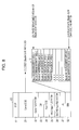
- FIG. 8 is a diagram explaining bad block management according to a second embodiment.
- FIG. 9 is a block diagram illustrating a configuration example of a portable terminal as a memory management apparatus employing a memory management method according to an embodiment.
- FIG. 1 is a block diagram illustrating a configuration example of a memory management apparatus employing a memory management method (bad block management: BBM) according to the first embodiment.
- BBM bad block management
- the memory management apparatus 10 includes a control unit 11 , a NAND memory 12 , a SDRAM (Synchronous Dynamic Random Access Memory) 13 , and buses 14 and 15 .
- the control unit 11 includes a processor such as a CPU (Central Processing Unit) or a DSP (Digital Signal Processor) and performs processing of the memory management apparatus 10 and control of each element.
- the control unit 11 has a function as a NAND driver 11 a , which performs data communication with respect to the NAND memory 12 through the bus 14 , and a function as a SDRAM driver 11 b , which performs data communication with respect to the SDRAM 13 of a working memory through the bus 15 .
- the NAND memory 12 is a rewritable non-volatile memory that stores programs executed by the control unit 11 .
- the NAND memory 12 roughly includes a code area 12 a that stores code (program code) of a program itself and a storage area 12 b that stores files for updating.
- the storage area 12 b can store various pieces of data such as a phone book, electronic mail, web content, music or image in addition to programs.
- the content of the code area 12 a is extracted (copied) to the SDRAM 13 during booting (start), and the programs are executed on the SDRAM 13 .
- the content (program) of the boot area of the NAND memory 12 is executed after being read to the memory area in the control unit 11 by the embedded logic of the control unit 11 .
- the program includes an algorithm for executing the memory management method according to the first embodiment.
- Program code to be executed by the program is extracted to the SDRAM 13 from the NAND memory 12 , and the programs are executed on the SDRAM 13 .
- an update file is created in advance by a dedicated tool external to the memory management apparatus 10 , is downloaded from a dedicated server through a communication unit (not shown), and is stored in the storage area 12 b of the NAND memory 12 .
- a loader 16 is configured to load programs to the NAND memory 12 through the control unit 11 at the time of program upgrade such that the programs are stored therein. For example, data communication between the control unit 11 and the loader 16 is performed using a UART (Universal Asynchronous Receiver Transmitter) or a USB interface.
- UART Universal Asynchronous Receiver Transmitter
- USB interface Universal Asynchronous Receiver Transmitter
- FIG. 2 illustrates one example of a binary image of data preserved in the NAND memory.
- the binary image 20 of the example includes a common code (Commcode) 21 , a common file system (Commfilesystem) 22 , a DSP 23 , application software code (Appscode) 24 , a first application software file system (first Appsfilesystem) 25 , a second application software file system (second Appsfilesystem) 26 , and a Log 27 .
- the binary image will be called a “partition table” later.
- the common code 21 is an area that includes code (programs) used when the memory management apparatus 10 communicates with the outside. Furthermore, the common file system 22 is an area that includes data such as parameters according to communication.
- the DSP 23 is an area that includes codes of firmware for driving a DSP of the control unit 11 and parameters.
- the application software code 24 is an area that includes codes (programs) of application software. Furthermore, the first application software file system 25 and the second application software file system 26 are areas that include data generated by executing the application software.
- the Log 27 is an area that includes an operation history of the control unit 11 .
- the binary image 20 for example, includes a boot area (not shown) and the like.
- ID# in the binary image 20 illustrated in FIG. 2 is basically made to correspond to the physical addresses of the NAND memory.
- One solution for appropriately performing the BBM is to select IDs 1 , 3 and 4 as areas to which the BBM is applicable and select IDs 2 , 5 and 6 as areas to which the BBM is not applicable.
- the reason for selecting the IDs 2 , 5 and 6 as the areas, to which the BBM is not applicable, is because data of the areas is managed by the file system.
- the structure of the file system mainly includes an information management table, a storage area (user data), and a preliminary area prepared for the case where a bad area occurs.
- the common file system 22 includes an information management table 22 a , a storage area (user data) 22 b , and a preliminary area 22 c .
- the preliminary area 22 c is an area to be used when a bad area occurs in the storage area 22 b.
- the file system is configured to necessarily update the information management table if the storage area is accessed. That is, this means that it is necessary for the file system to prepare the preliminary area in the information management table in consideration of a case where a bad area occurs in the information management table.
- FIG. 4 illustrates a configuration example of the information management table.
- the information management table 22 a includes an information management table 22 a - 1 and a preliminary area 22 a - 2 .
- the preliminary area 22 a - 2 is an area to be used when a bad area occurs in the information management table.
- the initial number of bad blocks in a NAND memory is to be smaller than 2%.
- a “block” in the present application indicates a unit area with a specific size in each memory device.
- the generation of bad blocks differs by memory manufacturing companies and may be concentrated in the information management table and a preliminary area thereof.
- the initial maximum number of bad blocks is by design about 80 when considering a defect ratio of 2%. Therefore, in general, only a small number of blocks are allocated to a preliminary area guaranteed for the bad block.
- the bad block management according to the first embodiment is performed with respect to the information management table in the file system constituting the partition table of the NAND memory, and bad block management provided in the file system as one function is further performed with respect to the user data in the file system.
- a bad block is detected by the process (program update) at the time of erasing or writing
- the bad block is replaced with a preliminary memory area (e.g., a replacement area) prepared in advance.
- a preliminary memory area e.g., a replacement area
- write remapping is preferably applied to an access process (refer to FIG. 7 ) to the NAND memory when it is highly necessary to reliably resolve an initial bad block by using a replacement area.
- the bad block When a bad block is detected by the process at the time of erasing or writing, the bad block is simply skipped over and shift to the next block is performed in order to find the next good block without replacing the bad block with a preliminary memory area (e.g., a replacement area) prepared in advance. However, access to the shifted block is performed through the preliminary memory area prepared in advance.
- the write mapping is preferably applied to an access process (refer to FIG. 7 ) to the NAND memory when the necessity of removing an initial bad block without using a replacement area (while saving the replacement area) is relatively high.
- the bad block When a bad block is detected by erasing or writing execution, the bad block is simply skipped over and shift to the next block is performed in order to find the next good block regardless of the preliminary memory area (e.g., the replacement area) prepared in advance. In this access process, the BBM is not correlated.
- mapping table a physical/logical address conversion table
- a designated block is read.
- the BBM is not correlated.
- a combination of write remapping and write mapping is a novel concept proposed by the applicant. Hereinafter, the concept will be described with reference to FIG. 5 .
- FIG. 5 is a diagram explaining a block conversion concept in the NAND memory according to the first embodiment.
- the NAND memory 12 illustrated in FIG. 5 ensures a replacement area as an area for replacing a bad block.
- FIG. 5 when a block A is detected as a bad block, the block A is changed to a block A′ allocated to the replacement area by write remapping. In a similar manner, a block B is also changed to a block B′ allocated to the replacement area. The block A and the block B are not used. In addition, when a bad block is detected in the block B′, shift to a next good block in the replacement area is performed.
- the block B (an actual block is B′) has already changed to a bad block
- the block B is detected as a bad block.
- the block B is changed to the block C by write mapping.
- the block C is skipped over and the next block D is selected by write mapping.
- the information management table and the preliminary area are used to manage management information such as “corresponding information of a replacement destination” or the “bad block information in an area for management” as illustrated in Japanese Unexamined Patent Application Publication No 2008-40701 (refer to FIG. 7 ) as one example.
- the management information is stored in blocks of physical addresses of the NAND memory corresponding to the logical addresses of the file system.
- the “corresponding information of the replacement destination” represents a correspondence relationship thereof.
- the block number of the bad block and the block number of the replacement area are made to correspond to each other for management.
- a management area, an interference area, and a replacement area are areas for management.
- “Bad block information in the areas for management” is information (herein, block number) for specifying a bad block which is recorded when a block of any one of the areas for management is defective.
- FIG. 6 is a diagram illustrating a relationship between areas corresponding to the logic addresses of the file system and blocks corresponding to the physical addresses of the NAND memory according to the first embodiment.
- binary data recorded in the NAND memory 12 includes a file system 30 - 1 , which employs a logic address 0X . . . 00 as a start address, and a file system 30 - 2 , which employs a logic address 0X . . . 01 as a start address.
- the process for replacing the area 31 A of the information management table with a block 35 B of the replacement area of the NAND memory 12 is write remapping.
- the process for changing the block 35 B to an area 32 A of the preliminary area of the file system 30 - 1 without using a preliminary area anew is write mapping.
- write remapping is combined with write mapping, resulting in a change in the use rate of the preliminary area in the file system and the preliminary area and the NAND memory. That is, when a block of the NAND memory corresponding to an arbitrary area of the information management table is defective, the block is changed to the replacement area without using the preliminary area in the case of applying write remapping whereas the preliminary area is used in the case of applying write mapping.
- the bad block management disclosed in the first embodiment is performed. After the program codes in the NAND memory are transmitted to the SDRAM in units of blocks, the bad block management provided in the file system as one function is applied.
- FIG. 7 is a diagram explaining the bad block management (the selective BBM) according to the first embodiment.
- a typical boot process of the NAND memory will be described as one example.
- the common code 21 and the application software code 24 are transmitted to the SDRAM 13 from the NAND memory 12 at the time of start and programs are executed in the SDRAM 13 after all codes are transmitted.
- an example of the selective BBM according to the process content will be described.
- the binary data of the ID 1 (the common code 21 ), the ID 2 (the common file system 22 ), the ID 3 (the DSP 23 ) and the ID 4 (the application software code 24 ) are loaded to the NAND memory 12 .
- the control unit 11 is configured to apply write remapping to the ID 1 to ID 4 for the loader 41 and replace all initial bad blocks with replacement areas.
- the binary data of the ID 5 (the first application software file system 25 ), the ID 6 (the second application software file system 26 ), and the ID 7 (the Log 27 ) are loaded to the NAND memory 12 .
- the control unit 11 is configured to apply the write w/o mapping to the ID 5 to ID 7 for the loader 42 and perform the bad block management by the file system other than the selective BBM.
- the binary data of the ID 2 and ID 4 is performed with respect to the NAND memory 12 .
- the control unit 11 is configured to apply the write mapping to the ID 2 and ID 4 for the common code 45 and perform access to the NAND memory 12 via the preliminary memory area (e.g., the replacement area) prepared in advance. However, a bad block is not replaced.
- the binary data of the ID 5 to ID 7 is performed with respect to the NAND memory 12 .
- the control unit 11 is configured to apply the writing w/o mapping to the ID 5 to ID 7 for the application soft code 44 and perform the bad block management by the file system other than the selective BBM.
- the control unit 11 is configured to apply the read mapping to process elements having write remapping and write mapping functions.
- the read mapping is applied to the loader 41 , the boot 43 , the common code 45 and the FOTA (Firmware Over The Air) 46 .
- the boot 43 is a process for temporarily copying information in the NAND memory to the SDRAM.
- the FOTA represents downloading of an update program to a portable terminal via a wireless network.
- the control unit 11 is configured to apply the read w/o mapping to process elements having the write w/o mapping function.
- the read w/o mapping is applied to the loader 42 and the application soft code 44 .
- a bad block can be replaced with the preliminary memory area (e.g., the replacement area) prepared in advance by applying write remapping to all ID#.
- the selective BBM can be adapted to any combinations.
- the selective BBM can be performed using the combination of write remapping and write mapping.
- the bad blocks are replaced with the preliminary memory area (e.g., the replacement area) prepared in advance. Consequently, even if the bad blocks are concentrated in the information management table, no problems occur in the actual access process to the NAND memory.
- all preliminary areas for the information management table include a plurality of blocks which are treated as good blocks.
- the difference between the memory management method (the selective BBM) according to the first embodiment and the existing approach for the BBM will be further described more clearly.
- description will be given on the assumption that the common file system is included in the area to which the BBM is applicable.
- all functions of the BBM are to be performed when common codes operate.
- this means that a complicated design is necessary in order to avoid a collision between the BBM performed outside the file system and operation of the file system which performs the BBM as a function provided therein.
- the selective BBM of the first embodiment the initial bad block is converted to the preliminary memory area prepared in advance, which is simply performed as a function of the file system. As a result, a complicated structure for adjusting the collision on the bad block management is not necessary, and the BBM can be applied to the file system by using a simple configuration.
- each memory management apparatus which accesses the NAND driver 11 a (refer to FIG. 1 ), will be described.
- the control unit 11 is configured to perform the access process according to the partition table (e.g., the binary image 20 of FIG. 2 ).
- the partition table is stored in the NAND memory 12 and the control unit 11 , for example, selects modes (write remapping, write mapping and the like) of the access process for each process element defined in FIG. 7 . Even if the partition table is not be received, the control unit 11 can recognize the mode of the access process in advance and operate according to the system design.
- a NAND driver for processing the common code and the application software code may vary depending on memory management apparatuses.
- the memory management method (the selective BBM) according to the first embodiment can be applied to the invention disclosed in Japanese Unexamined Patent Application Publication No 2008-40701.
- the invention disclosed in Japanese Unexamined Patent Application Publication No 2008-40701 can be adapted to write remapping, write mapping and read mapping functions according to the first embodiment.
- the second embodiment an example in which the memory management method according to the first embodiment is applied to the invention disclosed in Japanese Unexamined Patent Application Publication No 2008-40701 will be described.
- FIG. 8 is a diagram explaining bad block management according to the second embodiment.
- the first embodiment is an example in which the information management table and the preliminary area thereof in the file system are used for the bad block management.
- an area for the bad block management is provided outside the file system and management of a bad block and block replacement management are performed by storing management information in the area.
- a binary image 50 further includes areas for a boot 51 and a BBM 52 differently from the binary image 20 (refer to FIG. 2 ).
- the BBM 52 is an area which manages management information for managing the bad block.
- a block of the NAND memory 12 corresponding to the BBM 52 of the binary image 50 is divided into a “BBM management area”, an “interference area” and a “replacement area”.
- the BBM management area is an area which stores management information for managing the bad block and the replacement block of the NAND memory 12 .
- the management information includes the “corresponding information of the replacement destination” or the “bad block information in an area for management” as illustrated in Japanese Unexamined Patent Application Publication No 2008-40701 (refer to FIG. 7 ) as one example.
- the interference area is an area used in order to distinguish the boundary between the BBM management area and the replacement area.
- the replacement area is guaranteed as an area for replacing the bad block.
- BlockN+3 When it is determined that a defect is detected in a BlockN+3 of the NAND memory 12 corresponding to the common code 21 of the binary image 50 and writing may not be possible, the BlockN+3 is marked as a bad block and prohibited from being used.
- a code to be written in the BlockN+3 is written in a BlockN+M (a replacement area M ⁇ 4) of the NAND memory 12 corresponding to the BBM 52 , instead of the next BlockN+4, which is called write remapping.
- the replacement information is stored in a BlockN (a BBM management area 1 ) of the NAND memory 12 corresponding to the BBM 52 .
- the replacement area M ⁇ 4 stores replacement information for replacing the BlockN+3.
- the bad block When the bad block is detected as described above, the bad block is replaced with the replacement area and management information of the BBM management area, which defines address conversion of physical addresses/logical addresses, is updated.
- the bad block and the replacement block are managed using the management information, so that it is possible to allow actual physical addresses to correspond to logical addresses and to perform the address conversion for converting the logical addresses into the physical addresses.
- the BBM 52 which is an area for the bad block management, is provided outside the file system, so that an area (e.g., a preliminary area) for the bad block management in the file system can be small, resulting in an increase in a storage area.
- FIG. 9 is a block diagram illustrating a configuration example of a portable terminal as a memory management apparatus to which the memory management method of an embodiment is applied.
- the same reference numerals are used to designate the same elements as those of the memory management apparatus 10 illustrated in FIG. 1 , and detailed thereof will be omitted.
- the portable terminal 60 includes the control unit 11 , a voice processing unit 61 , a microphone 62 , a speaker 63 , the NAND memory 12 , the SDRAM 13 , a communication unit 64 , a duplexer 65 , an antenna 66 , and an operation unit 67 , and a display unit 68 .
- the voice processing unit 61 is configured to perform a voice process such as communication or music play under the control of the control unit 11 , receive audio data from the microphone 62 , and output audio data to the speaker 63 .
- the control unit 11 has a processor such as a CPU (Central Processing Unit) or a DSP (Digital Signal Processor), and performs processes of the portable terminal 10 and control of each element.
- the voice processing unit 61 is configured to perform a voice process such as communication or music play under the control of the control unit 11 , receive audio data from the microphone 62 , and output audio data to the speaker 63 .
- the communication unit 64 is an element that performs wireless transmission/reception with respect to a base station (not shown) through the antenna 66 and the duplexer 65 under the control of the control unit 11 .
- the operation unit 67 has ten keys, various control keys and the like, and has a function of inputting instructions or information by a user to the control unit 11 .
- the display unit 68 for example, has a display device such as an LCD or an organic EL, and has a function of displaying visible information such as text or images (still images and moving images) with respect to a user.
- the claimed invention is not limited to the previous embodiments as described above. That is, it goes without saying that various modifications and applications can be made without departing from the scope and spirit of the invention as disclosed in the accompanying claims.
- a cellular phone terminal has been described as an example.
- the portable terminal is not limited to a phone terminal.
- the present specification can be applied to the case where it is generally necessary to rewrite the content of a block of a part of a NAND memory without having influence on other blocks.
- the present specification is preferably applied to a NAND type flash memory.
- the present specification may be applied to a NOR type flash memory.
- an OS Operating System
- an OS Operating System
Landscapes
- Engineering & Computer Science (AREA)
- Theoretical Computer Science (AREA)
- Physics & Mathematics (AREA)
- General Engineering & Computer Science (AREA)
- General Physics & Mathematics (AREA)
- Techniques For Improving Reliability Of Storages (AREA)
Abstract
Description
Claims (10)
Priority Applications (1)
| Application Number | Priority Date | Filing Date | Title |
|---|---|---|---|
| US13/105,538 US8706954B2 (en) | 2010-09-07 | 2011-05-11 | Memory management apparatus and memory management method |
Applications Claiming Priority (2)
| Application Number | Priority Date | Filing Date | Title |
|---|---|---|---|
| US38057610P | 2010-09-07 | 2010-09-07 | |
| US13/105,538 US8706954B2 (en) | 2010-09-07 | 2011-05-11 | Memory management apparatus and memory management method |
Publications (2)
| Publication Number | Publication Date |
|---|---|
| US20120059979A1 US20120059979A1 (en) | 2012-03-08 |
| US8706954B2 true US8706954B2 (en) | 2014-04-22 |
Family
ID=45771496
Family Applications (1)
| Application Number | Title | Priority Date | Filing Date |
|---|---|---|---|
| US13/105,538 Active 2032-03-06 US8706954B2 (en) | 2010-09-07 | 2011-05-11 | Memory management apparatus and memory management method |
Country Status (1)
| Country | Link |
|---|---|
| US (1) | US8706954B2 (en) |
Families Citing this family (2)
| Publication number | Priority date | Publication date | Assignee | Title |
|---|---|---|---|---|
| US11735286B2 (en) * | 2021-09-30 | 2023-08-22 | Innogrit Technologies Co., Ltd. | Selecting read reference voltage using historical decoding information |
| CN113688070A (en) * | 2021-10-27 | 2021-11-23 | 苏州浪潮智能科技有限公司 | Method, device and equipment for replacing bad block in NAND and readable medium |
Citations (6)
| Publication number | Priority date | Publication date | Assignee | Title |
|---|---|---|---|---|
| US5860082A (en) * | 1996-03-28 | 1999-01-12 | Datalight, Inc. | Method and apparatus for allocating storage in a flash memory |
| US6260156B1 (en) * | 1998-12-04 | 2001-07-10 | Datalight, Inc. | Method and system for managing bad areas in flash memory |
| US7295479B2 (en) * | 2003-04-04 | 2007-11-13 | Samsung Electronics Co., Ltd. | Apparatus and method for managing bad blocks in a flash memory |
| JP2008040701A (en) | 2006-08-04 | 2008-02-21 | Sony Ericsson Mobilecommunications Japan Inc | Memory management method and portable terminal equipment |
| US20090138754A1 (en) * | 2007-11-28 | 2009-05-28 | David Alan Edwards | Memory Errors |
| US7797693B1 (en) * | 2003-12-12 | 2010-09-14 | Hewlett-Packard Development Company, L.P. | NAND mobile devices capable of updating firmware or software in a manner analogous to NOR mobile devices |
-
2011
- 2011-05-11 US US13/105,538 patent/US8706954B2/en active Active
Patent Citations (6)
| Publication number | Priority date | Publication date | Assignee | Title |
|---|---|---|---|---|
| US5860082A (en) * | 1996-03-28 | 1999-01-12 | Datalight, Inc. | Method and apparatus for allocating storage in a flash memory |
| US6260156B1 (en) * | 1998-12-04 | 2001-07-10 | Datalight, Inc. | Method and system for managing bad areas in flash memory |
| US7295479B2 (en) * | 2003-04-04 | 2007-11-13 | Samsung Electronics Co., Ltd. | Apparatus and method for managing bad blocks in a flash memory |
| US7797693B1 (en) * | 2003-12-12 | 2010-09-14 | Hewlett-Packard Development Company, L.P. | NAND mobile devices capable of updating firmware or software in a manner analogous to NOR mobile devices |
| JP2008040701A (en) | 2006-08-04 | 2008-02-21 | Sony Ericsson Mobilecommunications Japan Inc | Memory management method and portable terminal equipment |
| US20090138754A1 (en) * | 2007-11-28 | 2009-05-28 | David Alan Edwards | Memory Errors |
Also Published As
| Publication number | Publication date |
|---|---|
| US20120059979A1 (en) | 2012-03-08 |
Similar Documents
| Publication | Publication Date | Title |
|---|---|---|
| US7882301B2 (en) | Wear leveling in storage devices based on flash memories and related circuit, system, and method | |
| US7454670B2 (en) | Data management apparatus and method of flash memory | |
| US20170315925A1 (en) | Mapping table loading method, memory control circuit unit and memory storage apparatus | |
| TWI442228B (en) | Storage device wear leveling | |
| US7797573B2 (en) | Memory management method and portable terminal device | |
| US7577783B2 (en) | Portable data storage device and method of dynamic memory management therefor | |
| US20100125772A1 (en) | Error correcting controller, flash memory chip system, and error correcting method thereof | |
| JP2007199905A (en) | Method for controlling semiconductor storage device | |
| JP2017527877A (en) | Method and apparatus for reading / writing data from / to flash memory and user equipment | |
| US9037773B2 (en) | Methods for processing and addressing data between volatile memory and non-volatile memory in an electronic apparatus | |
| US8706954B2 (en) | Memory management apparatus and memory management method | |
| KR100456736B1 (en) | Method for reducing booting time of a digital device having a flash memory | |
| US20130019056A1 (en) | Data Storing Method and Apparatus Applied to Flash Memory Storage Device | |
| US10289334B2 (en) | Valid data merging method, memory controller and memory storage apparatus | |
| JP2006011533A (en) | Memory card, semiconductor device, and control method of semiconductor memory | |
| JP2004326165A (en) | Device and method for controlling memory | |
| US20120303879A1 (en) | Memory Device and Method for Programming Flash Memory Utilizing Spare Blocks | |
| US7979606B2 (en) | Method for storing data | |
| JP2007233838A (en) | Control method for memory system | |
| CN111813708B (en) | Block mapping system and method for storage device | |
| JP2009134672A (en) | Memory management method and portable terminal equipment | |
| JP2007280329A (en) | Nonvolatile storage device and method for managing the same device | |
| JP5424574B2 (en) | Navigation device | |
| US10261899B2 (en) | Method, device and system for data processing using dedicated mapping between logical and physical addresses | |
| CN101149972B (en) | FLASH memory chip with a plurality of separate operation memory space |
Legal Events
| Date | Code | Title | Description |
|---|---|---|---|
| AS | Assignment |
Owner name: SONY MOBILE COMMUNICATIONS AB, SWEDEN Free format text: CHANGE OF NAME;ASSIGNOR:SONY ERICSSON MOBILE COMMUNICATIONS AB;REEL/FRAME:028081/0600 Effective date: 20120221 |
|
| AS | Assignment |
Owner name: SONY CORPORATION, JAPAN Free format text: ASSIGNMENT OF PARTIAL RIGHTS;ASSIGNOR:SONY MOBILE COMMUNICATIONS AB;REEL/FRAME:032310/0081 Effective date: 20140108 |
|
| STCF | Information on status: patent grant |
Free format text: PATENTED CASE |
|
| FEPP | Fee payment procedure |
Free format text: PAYOR NUMBER ASSIGNED (ORIGINAL EVENT CODE: ASPN); ENTITY STATUS OF PATENT OWNER: LARGE ENTITY |
|
| AS | Assignment |
Owner name: SNAPTRACK, INC., CALIFORNIA Free format text: ASSIGNMENT OF ASSIGNORS INTEREST;ASSIGNORS:SONY CORPORATION;SONY MOBILE COMMUNICATIONS INC.;REEL/FRAME:037027/0399 Effective date: 20151026 |
|
| AS | Assignment |
Owner name: SONY MOBILE COMMUNICATIONS INC., JAPAN Free format text: ASSIGNMENT OF ASSIGNORS INTEREST;ASSIGNOR:SONY MOBILE COMMUNICATIONS AB;REEL/FRAME:037593/0001 Effective date: 20150928 |
|
| AS | Assignment |
Owner name: SONY ERICSSON MOBILE COMMUNICATIONS JAPAN, INC., J Free format text: ASSIGNMENT OF ASSIGNORS INTEREST;ASSIGNORS:AOYAGI, KATSUMI;LJUNDQVIST, RUTGER;WACHTMEISTER, HANS;AND OTHERS;SIGNING DATES FROM 20100914 TO 20100927;REEL/FRAME:037647/0144 Owner name: SONY ERICSSON MOBILE COMMUNICATIONS AB, SWEDEN Free format text: ASSIGNMENT OF ASSIGNORS INTEREST;ASSIGNORS:AOYAGI, KATSUMI;LJUNGQVIST, RUTGER;WACHTMEISTER, HANS;AND OTHERS;SIGNING DATES FROM 20100914 TO 20100927;REEL/FRAME:037648/0757 Owner name: SONY ERICSSON MOBILE COMMUNICATIONS JAPAN, INC., J Free format text: ASSIGNMENT OF ASSIGNORS INTEREST;ASSIGNORS:AOYAGI, KATSUMI;LJUNGQVIST, RUTGER;WACHTMEISTER, HANS;AND OTHERS;SIGNING DATES FROM 20100914 TO 20100927;REEL/FRAME:037648/0757 |
|
| AS | Assignment |
Owner name: SONY MOBILE COMMUNICATIONS INC., JAPAN Free format text: ASSIGNMENT OF ASSIGNORS INTEREST;ASSIGNOR:SONY MOBILE COMMUNICATIONS AB;REEL/FRAME:037695/0952 Effective date: 20150928 |
|
| AS | Assignment |
Owner name: SONY ERICSSON MOBILE COMMUNICATIONS AB, SWEDEN Free format text: CORRECTIVE ASSIGNMENT TO CORRECT THE ASSIGNOR NAME PREVIOUSLY RECORDED AT REEL: 037648 FRAME: 0757. ASSIGNOR(S) HEREBY CONFIRMS THE ASSIGNMENT;ASSIGNOR:SONY ERICSSON MOBILE COMMUNICATIONS JAPAN, INC.;REEL/FRAME:037810/0015 Effective date: 20101019 |
|
| MAFP | Maintenance fee payment |
Free format text: PAYMENT OF MAINTENANCE FEE, 4TH YEAR, LARGE ENTITY (ORIGINAL EVENT CODE: M1551) Year of fee payment: 4 |
|
| MAFP | Maintenance fee payment |
Free format text: PAYMENT OF MAINTENANCE FEE, 8TH YEAR, LARGE ENTITY (ORIGINAL EVENT CODE: M1552); ENTITY STATUS OF PATENT OWNER: LARGE ENTITY Year of fee payment: 8 |