US8705986B2 - PMD-insensitive method of chromatic dispersion estimation for a coherent receiver - Google Patents
PMD-insensitive method of chromatic dispersion estimation for a coherent receiver Download PDFInfo
- Publication number
- US8705986B2 US8705986B2 US12/926,533 US92653310A US8705986B2 US 8705986 B2 US8705986 B2 US 8705986B2 US 92653310 A US92653310 A US 92653310A US 8705986 B2 US8705986 B2 US 8705986B2
- Authority
- US
- United States
- Prior art keywords
- chromatic dispersion
- parameter
- frequency
- domain data
- outputs
- Prior art date
- Legal status (The legal status is an assumption and is not a legal conclusion. Google has not performed a legal analysis and makes no representation as to the accuracy of the status listed.)
- Active, expires
Links
Images


Classifications
-
- H—ELECTRICITY
- H04—ELECTRIC COMMUNICATION TECHNIQUE
- H04B—TRANSMISSION
- H04B10/00—Transmission systems employing electromagnetic waves other than radio-waves, e.g. infrared, visible or ultraviolet light, or employing corpuscular radiation, e.g. quantum communication
- H04B10/60—Receivers
- H04B10/61—Coherent receivers
- H04B10/616—Details of the electronic signal processing in coherent optical receivers
- H04B10/6161—Compensation of chromatic dispersion
-
- H—ELECTRICITY
- H04—ELECTRIC COMMUNICATION TECHNIQUE
- H04B—TRANSMISSION
- H04B10/00—Transmission systems employing electromagnetic waves other than radio-waves, e.g. infrared, visible or ultraviolet light, or employing corpuscular radiation, e.g. quantum communication
- H04B10/60—Receivers
- H04B10/61—Coherent receivers
- H04B10/616—Details of the electronic signal processing in coherent optical receivers
- H04B10/6162—Compensation of polarization related effects, e.g., PMD, PDL
Definitions
- Coherent optical communication systems have been developed that provide distinct advantages over more traditional direct detection schemes.
- the optical phase and amplitude of a transmitted optical signal can be detected, thus enabling the use of multilevel modulation schemes to increase optical fiber spectral efficiency.
- Coherent detection provides another advantage over direct detection in that linear impairments of the transmitted optical signal can be compensated for in the receiver using digital filters and other known digital compensation techniques.
- Some important linear impairments that can affect the performance of optical communication systems include two forms of signal distortion resulting from chromatic dispersion (CD) and polarization mode dispersion (PMD) of the optical signal.
- the transmitted optical signal has a finite spectral width such that the spectral components may be transmitted at different frequencies.
- Chromatic dispersion is a result of the different spectral components propagating at different speeds along the fiber, resulting in an undesirable temporal spreading of the optical signal.
- PMD occurs due to the different polarization modes of the optical signal propagating along the fiber at different speeds and is affected by environmental effects and asymmetries in the optical fiber, which are often random, unpredictable and can vary over time. Due to the random and unpredictable nature of PMD, PMD cannot be easily determined or compensated for in a conventional optical communication system.
- Optical communication systems generally include a number of links of optical fibers and optical system components, each contributing to the overall chromatic dispersion of received signals.
- the effects of chromatic dispersion are linear and deterministic and can be more easily compensated for than the effects of PMD.
- One conventional method of compensating for chromatic dispersion in an optical communication system includes the use of dispersion compensation fibers (DCFs) or other components that compensate chromatic dispersion optically.
- DCFs dispersion compensation fibers
- implementing such DCFs and other known dispersion compensating techniques and components in the optical communication system undesirably increases the size of the system, and can be cumbersome and expensive. Additionally, such dispersion compensation components can undesirably limit the power and spectral efficiency of the optical communication system.
- Some known methods for dealing with these impairments utilize a preset or adaptive filter to compensate for a known chromatic dispersion in the receiver. These solutions, however, are limited in that in many systems, especially switched systems in which the signal may travel via one of several different links, the chromatic dispersion effects cannot be easily known or determined in advance because each link scenario has a different chromatic dispersion, or the adaptive filter cannot be easily or efficiently updated.
- the chromatic dispersion may be estimated by iteratively scanning a range of chromatic dispersion values for the received signal until some control loops in the receiver are working, e.g., automatic gain control (AGC) and clock recovery loop.
- the scanning is performed by estimating a first value for the chromatic dispersion (such as 1000 ps/nm), calculating a chromatic dispersion coefficient, evaluating a receiver circuit response using the calculated chromatic dispersion coefficients in a compensation filter, then revising the estimate if necessary.
- AGC automatic gain control
- the range of the estimated chromatic dispersion values should be relatively narrow to minimize estimation error and ensure that the control loops work, that is, to ensure a clock phase detector has satisfactory sensitivity.
- the estimated chromatic dispersion value in each step should differ by 1000 ps/nm or less per step.
- the scan may require approximately 50 steps or iterations.
- the step of calculating the chromatic dispersion coefficients results in even greater complexity. Additionally, there is added delay in such systems due to the time required for the acquired signal to be allocated for the chromatic dispersion scanning steps discussed above.
- one known method proposes an adaptive algorithm for determining an equalizer metric in a frequency domain equalizer (FDE) to estimate the chromatic dispersion from the received signal.
- FDE frequency domain equalizer
- each of the transfer functions for a range of predetermined chromatic dispersion values are determined and pre-stored in a look-up table to reduce complexity at the receiver.
- Second order PMD is characterized as the derivative of the first order PMD with respect to frequency. Because second order PMD is a function of frequency, it mimics chromatic dispersion. If the estimated chromatic dispersion in these known methods includes the effects of second order PMD, the receiver sensitivity can be seriously corrupted.
- a method for compensating chromatic dispersion in a received optical signal in which a plurality of outputs of a Fourier transform circuit supply frequency domain data in response to time domain data associated with the optical signal.
- a first parameter is determined based on components of the frequency data supplied from selected ones of the plurality of outputs of the Fourier transform circuit, said first parameter being indicative of a phase difference between selected ones of the plurality of components.
- a second parameter that is indicative of a chromatic dispersion of the optical signal is determined based on said first parameter. Then, a frequency response of the chromatic dispersion based on said second parameter is determined and said plurality of outputs of the frequency domain representation of the received signal are processed based on the frequency response of the chromatic dispersion.
- a method of compensating chromatic dispersion of a received optical signal supplies an analog signal in response to the received optical signal.
- the analog signal is sampled to provide time domain data with an associated baud frequency, which is supplied to a Fourier transform circuit.
- a number of first parameters are calculated from a plurality of respective subsets of frequency domain data output from the Fourier transform circuit, each of said subsets include a first and second sample of the frequency domain data offset from each other by a value indicative of the baud frequency.
- the method determines a linear phase of a time averaged value of each of said respective first parameters over a predetermined time period and calculates a second parameter indicative of a chromatic dispersion of the optical signal based on the linear phase of each of the plurality of said time averaged values, said second parameter being indicative of a linear slope of said plurality of linear phases.
- a method compensates chromatic dispersion by first estimating a value indicative of a chromatic dispersion of an optical signal based on a subset of a frequency domain data of a received signal. A frequency response of the chromatic dispersion is then determined based on said value and the frequency domain data is multiplied by an inverse of the determined frequency response.
- a receiver comprising a Fourier transform circuit comprising a plurality of outputs of frequency domain data in response to time domain data associated with a received optical signal.
- the receiver further comprises a first module configured to determine a first parameter based on components of the frequency data supplied from selected ones of the plurality of outputs of the Fourier transform circuit, said first parameter being indicative of a phase difference between selected ones of the plurality of components.
- a second module is also provided that is configured to determine a second parameter indicative of a chromatic dispersion of the optical signal based on said first parameter, and to determine a frequency response of the chromatic dispersion based on said second parameter.
- the receiver further comprises a third module configured to process said plurality of outputs of the frequency domain representation of the received signal based on the frequency response of the chromatic dispersion.
- a system comprising a receiver configured to receive an optical signal and supply an analog signal in response to the optical signal.
- the receiver further comprises a first component configured to sample the analog signal to provide time domain data with an associated baud frequency and supply the time domain data to a Fourier transform circuit, and a second component configured to calculate a number of first parameters from a plurality of respective subsets of frequency domain data output from the Fourier transform circuit, each of said subsets including a first and second sample of the frequency domain data offset from each other by a value indicative of the baud frequency.
- a third component is also provided in the receiver to determine a linear phase of a time averaged value of each of said respective first parameters over a predetermined time period, and calculate a second parameter indicative of a chromatic dispersion of the optical signal based on the linear phase of each of the plurality of said time averaged values, said second parameter being indicative of a linear slope of said plurality of linear phases.
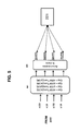
- FIG. 1 is a block diagram illustrating a coherent receiver consistent with an aspect of the present disclosure
- FIG. 2 is a diagram of a sample signal spectrum used to demonstrate the concept of CD estimation consistent with an aspect of the present disclosure
- FIG. 3 is a graph depicting the modeled performance of the CD estimate determined with respect to the sample signal illustrated in FIG. 2 consistent with an aspect of the present disclosure
- FIG. 4 is a diagram of a sample signal spectrum of a polarization multiplexed signal used to estimate the CD consistent with an aspect of the present disclosure
- FIG. 5 is a block diagram of the CD estimation circuit consistent with an aspect of the present disclosure.
- FIG. 6 is a flow diagram illustrating the steps performed in estimating chromatic dispersion consistent with the present disclosure.
- a method for estimating and compensating chromatic dispersion in a coherent receiver, and an optical communication system using the method is provided that is insensitive to PMD.
- a Fourier transform circuit provides, from a plurality of outputs, frequency domain data based on time domain data associated with a received optical signal.
- a phase difference between each of a number of pairs of related outputs of the frequency domain data is determined by computing the dot product of the related outputs.
- Each of the related outputs are offset from each other in the frequency domain by a value proportional to a sampling frequency, the outputs being related in that they comprise the same data spectrum.
- the dot product for each pair of related outputs yields a component of the data spectrum of the related outputs, a linear component of the phase difference between the related outputs, and a DC component of the phase difference.
- the data spectrum component is reduced to a constant value.
- An estimate for the chromatic dispersion is then calculated based on a linear slope of the time-averaged dot products.
- a chromatic dispersion estimate is calculated that is insensitive to PMD and other polarization effects in the optical communication system by determining the determinant of a linear system in which the PMD and polarization effects are represented, for example, using a Jones matrix. Because results in accordance with exemplary embodiments for estimating chromatic dispersion are insensitive to the PMD effects in the system, the calculated chromatic dispersion estimate is effective for compensating for the chromatic dispersion in the receiver, even if the PMD and other polarization effects are large.
- Methods and systems consistent with exemplary embodiments also enable a coherent receiver to efficiently detect a clock phase of the received signal together with a value for the chromatic dispersion, thus, increasing the receiver sensitivity and boosting performance of the overall optical communication system.
- FIG. 1 illustrates an embodiment of a coherent receiver 200 consistent with an aspect of the present disclosure.
- an incident optical signal S in is separated by a polarization beam splitter (PBS) 201 into first and second polarized signals of X and Y polarity, respectively.
- the polarized signals may be orthogonally polarized.
- the X polarity signal and the Y polarity signal are then respectively fed into two optical hybrids 203 and 205 together with a reference signal of a local oscillator optical signal output from a local oscillator laser 207 .
- Each optical hybrid ( 203 , 205 ) supplies optical signals to detector circuits 206 and 209 , each of which include known transimpedance amplifier and automatic gain control circuitry.
- Each of detector circuits 206 , 209 produces two base-band electrical signals linearly proportional to the in-phase (I) and quadrature (Q) components of the optical E-field on the X and Y polarity signals, respectively (i.e. XI, XQ and YI, YQ).
- XI, XQ and YI, YQ are analog signals which are next fed to analog to digital converters (A/D) circuits 213 , which may be within a digital signal processor (DSP) ASIC 211 .
- A/D circuits 213 output digital or digitized signals, as further shown in FIG. 1 .
- chromatic dispersion in optical communication systems can be represented by a linear function
- compensation of chromatic dispersion in a receiver consistent with the disclosed embodiments can be readily implemented using a finite impulse response filter (FIR) in the frequency domain, by determining an inverse frequency response of the chromatic dispersion.
- FIR finite impulse response filter
- chromatic dispersion estimation techniques consistent with exemplary embodiments are performed effectively in the frequency domain where they can be demonstrated to be insensitive to PMD.
- a plurality of Fast Fourier Transform (FFT) blocks or circuits 215 - 1 and 215 - 2 receive the digitized signals, supplied by A/D circuits 213 , which are all in the time domain, and output signals which are in the frequency domain.
- FFT Fast Fourier Transform
- a first FFT block 215 - 1 is used to transform the X polarity signals and a second FFT block 215 - 2 is used to transform the Y polarity signals.
- FFT blocks 215 - 1 and 215 - 2 have 256 outputs each, and thus may perform a 256 “point” transformation of the received signals, however, the present disclosure is not limited to this specific design and other methods of transforming the digital signals to the frequency domain could be used consistent with the present disclosure.
- FIG. 2 A sample 10 Gbaud data spectrum of the singularly polarized transmitted signal is shown in FIG. 2( a ).
- X U represents the random data spectrum in the upper side band of the X polarized transmitted signal
- X L represents the random data spectrum in the lower side band of the X polarized signal.
- the exemplary method determines a phase difference between related frequency domain data of the received signal as a function of frequency.
- the frequency domain data includes related data due to the up-sampling of the received signal, the data being related in that they include the same data spectrum.
- An illustrative up-sampled signal is shown in FIG. 2( b ).
- the 10 Gbaud signal spectrum is up-sampled by twice the baud rate or baud frequency so that it now spans over 20 Gbaud.
- the data from X U and X L is effectively copied as indicated by the dashed arrows in FIG. 2 , the copied data being spectrally spaced from one another by a value indicative of the baud frequency.
- a U and A L represent the same data spectrum as X U
- B U and B L represent the same data spectrum as X L .
- the exemplary embodiments are described herein using a 2 times up-sampling rate (2 samples per symbol), in practice, the exemplary embodiments may be realized using any sampling rate at least equal to or greater than the transmit baud rate, i.e. greater than or equal to 1 sample per symbol.
- the received signal is free from any PMD or other polarization rotation effects. Additionally, as shown in FIG. 2( b ), the received signal may have been modulated using some amplitude function represented by the curve shown. For the purpose of estimating chromatic dispersion in this embodiment, however, the amplitude function is also ignored.
- the upper and lower side bands of the up-sampled signal may be modeled in the frequency domain using equations 1 and 2 (Eqn. 1, 2), below.
- a U ( f 1 ) X U ( f 1 ) e j ⁇ 1 2 e ⁇ j ⁇ 1 (Eqn.
- a L ( f 2 ) X U ( f 2 ) e j ⁇ 2 2 e ⁇ j ⁇ 2 (Eqn. 2)
- X U (f) is the upper-side band (USB) data spectrum of the X polarity signal
- ⁇ is the chromatic dispersion coefficient
- ⁇ is the clock phase.
- a U and A L comprise the same data, and they differ only by ⁇ 1 and ⁇ 2 .
- each pair of frequencies (f 1 and f 2 ) will be represented by the singular value f.
- Similar representations for B U and B L which are copies of the lower side band data spectrum of X, can be written using the expressions shown in Eqn. 1 and Eqn. 2, respectively, by substituting X L for X U .
- the exemplary method is demonstrated by modeling only the expression of A U and A L as further discussed below.
- each data sample is processed by the FFT block 215 - 1 and corresponding frequency domain data is output.
- data processing by FFT block 215 - 1 can be modeled using Eqn. 1 and Eqn. 2 above. Because ⁇ represents the chromatic dispersion coefficient of the received signal, it is this value that the exemplary method determines. Upon determining a value for ⁇ , the effects of chromatic dispersion can be compensated for in the receiver by multiplying the outputs of FFT block 215 - 1 by the inverse frequency response e ⁇ j ⁇ 2 , as shown in FIG. 1 .
- the value for ⁇ is determined by comparing the phase differences between ⁇ 1 and ⁇ 2 over a desired number of frequencies. This phase difference is determined by calculating the dot product between A U and the complex conjugate of A L for each related pair of FFT outputs represented by frequencies (e.g. f 1 and f 2 ) as shown in Eqn. 3 below.
- the resultant vector may appear noisy due to the presence of the random data X U (f), and ⁇ cannot easily be determined. It can be shown, however, that
- 2 can be mitigated by calculating a time average of the dot product for each pair of frequencies over a desired number of clock cycles. For each clock cycle, the values for ⁇ , ⁇ 1 and ⁇ 2 for a selected pair of FFT 215 - 1 outputs (“frequency bins”) remain the same. X U , however, changes between clock cycles in each respective pair of frequency bins. Thus, averaging the dot product for each frequency pair over a predetermined period of time, i.e. over a number of clock cycles, preserves the phase information of the dot product while reducing the
- the averaging step is performed for at least 64 clock cycles.
- the averaging may be performed over any desired number of clock cycles, such as 4, 8, 16, 32, 64 or more, as discussed in greater detail below.
- the expression for the time average of the dot product for each frequency is shown by the angled brackets ⁇ > in Eqn. 3 below.
- 2 becomes a scalar.
- the phase difference of this time averaged quantity is more easily determined and is represented as ⁇ ( ⁇ 1 2 ⁇ 2 2 ) ⁇ ( ⁇ 1 ⁇ 2 ).
- ⁇ 1 ⁇ 2 2 ⁇ 10 GHz is a constant with respect to ⁇ 1
- ⁇ 1 2 ⁇ 2 2 is a linear function of ⁇ 1 or f. It follows then that the linear phase component, ⁇ 1 2 ⁇ 2 2 of the above quantity, is proportional to the chromatic dispersion coefficient ⁇ , and the DC constant portion of the quantity is proportional to the clock phase ⁇ .
- the chromatic dispersion in the optical communication system may be estimated in accordance with an exemplary embodiment. Since the value for ⁇ is proportional to the linear function of ⁇ 1 2 ⁇ 2 2 , the value for ⁇ is determined by calculating the linear slope of the time-averaged dot product in Eqn. 3 with respect to frequency. In other words, the value for ⁇ can be calculated by determining the rate of change of the calculated phase differences ⁇ 1 2 ⁇ 2 2 with respect to frequency. For example, in the exemplary embodiment using 256-pt FFT block 215 - 1 , the calculation in Eqn. 3 may be performed over 32 related outputs or frequency bin pairs of the 256 outputs from the FFT block 215 - 1 .
- the linear phase of the 32 resultant complex values are then graphed with respect to frequency and a linear slope of the graph is calculated. As noted above, this calculated linear slope is proportional to the value of ⁇ . This determined value is then used to calculate the coefficients associated with each frequency bin, which are input to the respective multipliers 219 shown in FIG. 1 .
- Eqn. 4 Another exemplary method for determining the value of ⁇ , without graphing the vectors, is shown in Eqn. 4, which provides that the estimate for chromatic dispersion is proportional to the angle of the sum of the differences for each calculation of the dot product from Eqn. 3 times the conjugate of the dot product shifted by ⁇ f, over all selected frequencies.
- Eqn. 4 is implemented in the microprocessor 221 shown in FIG. 1 .
- any method for calculating the linear slope of the dot product in Eqn. 3 with respect to frequency may be used to calculate the value for ⁇ , as would be understood by one of ordinary skill in the art.
- the time-averaged value of the dot product in Eqn. 3 yields a linear phase component and a DC constant phase component. Since the value for ⁇ is determined from a slope of the linear phase of the dot product in Eqn. 3, the exemplary method effectively ignores the DC constant phase component, thus, the chromatic dispersion estimate is not sensitive to any static clock phase ⁇ . Recovering the clock phase ⁇ enables the receiver clock to synchronize or “lock” with the clock of the transmitter of the received signal. Prior to “locking” the clock, however, the receiver clock may be offset from the transmit clock by up to 100 ppm, and in this case the clock phase ⁇ may not be static.
- the 100 ppm difference may result in a statistical variation of the parameter ‘ ⁇ ’ in the time averaging of the dot product of Eqn. 3 over a number of clock cycles. Therefore in practice, even though the exemplary method is insensitive to a static clock phase, the predetermined time or number of clock cycles used for averaging the dot product should be selected in consideration of the amount of clock offset.
- the averaging in Eqn. 3 does not yield any useful information. Therefore, with a 200 ppm clock offset, the number of clock cycles used in the averaging step should be reduced to say 16 or less. In turn, the smaller the amount of clock offset, the greater the number of clock cycles can be used during the time-averaging step. This concept is discussed in greater detail with respect to the second embodiment below.
- FIG. 3 depicts the performance of the estimated chromatic dispersion in this embodiment without PMD or other polarization effects with respect to the actual chromatic dispersion for a QPSK modulated system, or any modulation format, considering 10 dB OSNR, 8 MHz LW, 1 GHz frequency offset and 512 clock average.
- the estimated chromatic dispersion in this exemplary embodiment is nearly the same as the actual chromatic dispersion itself.
- the above disclosure provides exemplary embodiments for estimating a value of chromatic dispersion in an optical communication system for a single polarization signal.
- the received signal was modeled without considering the effect from PMD or other polarization rotation effects in the system.
- the results of the above exemplary embodiments can be extended to develop a chromatic dispersion estimate method that is insensitive to PMD in the optical communication system for a received signal with both X and Y polarizations.
- the individual steps of the following exemplary method are illustrated in the flow diagram of FIG. 6 , and are referred to throughout.
- a received signal is detected in the coherent receiver 200 , shown in FIG. 1 , and is up-sampled by the A/D converters 213 .
- the up-sampled digital signal is transformed into the frequency domain using FFT blocks 215 - 1 and 215 - 2 , as noted above.
- FIG. 4 illustrates the data spectra for a two polarization multiplexed signal which is used to expand the above exemplary embodiment that assumes no PMD, to a further exemplary embodiment where PMD effects are not negligible.
- the received data spectrum includes both X and Y polarization components, which “overlap” as shown in FIG. 4 . Similar to the discussion with respect to FIG.
- the 2 ⁇ (2 times) up-sampled data spectra for both the X and Y polarization can be represented as shown.
- a XU and A XL include the copied data spectrum from X U
- a YU and A YL include the copied data spectrum from Y U , the copied data spectrum being offset by a value indicative of the baud frequency.
- the received up-sampled signals are modeled including the effects of PMD and any other polarization rotation effects.
- the polarization rotations of the transmitted signal can be modeled using a Jones matrix as shown in Eqn. 5. Accordingly, as shown in the matrix representation of Eqn. 5 below, for the dual polarized signal, A XU is modeled as a function of X U and Y U times the corresponding elements in the Jones matrix, which is used to model the PMD in the optical communication system.
- ⁇ represents the phase of the received signal and ⁇ represents the polarization rotations of the received signal.
- the expanded form of the matrix representation in Eqn. 5 is shown in Eqn. 6 and Eqn. 8, below.
- [ Axu Ayu ] [ cos ⁇ ⁇ ⁇ ⁇ e - j ⁇ ⁇ ⁇ - sin ⁇ ⁇ ⁇ sin ⁇ ⁇ ⁇ cos ⁇ ⁇ ⁇ ⁇ e + j ⁇ ⁇ ⁇ ] ⁇ [ Xu Yu ] ( Eqn . ⁇ 5 )
- a XL and A YL signals which are expressed in expanded form in Eqn. 7 and Eqn. 9, respectively.
- the expressions for A XL and A YL differ from A XU and A YU only in the subscripts for ⁇ and ⁇ . This should be evident since A XL contains the same data spectrum as A XU , and A YL contains the same data spectrum as A YU , except that they are shifted by a frequency proportional to the up-sampling rate represented in FIG. 4 .
- the most general description of PMD is that it causes a different amount of polarization rotation induced on the signal at different frequencies. In Eqns.
- the frequency component in the upper side band is rotated by ⁇ 1 and ⁇ 1 and the frequency component in the lower side band is rotated by ⁇ 2 and ⁇ 2 .
- the upper and lower side bands for each of the X and Y polarized sample signals in the frequency domain can be written as shown below, where [1] indicates the frequency bin index of the FFT blocks, and ⁇ U is a shorthand notation representing the expression for e j ⁇ 1 2 e ⁇ j ⁇ 1 similar to Eqn. 1, and ⁇ L is a shorthand notation representing the expression for e j ⁇ 2 2 e ⁇ j ⁇ 2 similar to Eqn. 2.
- B XU , B XL , B YU and B YL which are copies of the lower side band data spectrum of X and Y, respectively, can be written using the expressions shown in Eqns. 6-9, respectively, by substituting X L for X U , and Y L for Y U .
- a XU [1] ( X U [1] cos ⁇ 1 e ⁇ j ⁇ 1 ⁇ Y U [1] sin ⁇ 1 ) ⁇ e j ⁇ U (Eqn.
- a XL [1] ( X U [1] cos ⁇ 2 e ⁇ j ⁇ 2 ⁇ Y U [1] sin ⁇ 2 ) ⁇ e j ⁇ L (Eqn. 7)
- a YU [1] ( X U [1] sin ⁇ 1 +Y U [1] cos ⁇ 1 e +j ⁇ 1 ) ⁇ e j ⁇ U (Eqn. 8)
- a YL [1] ( X U [1] sin ⁇ 2 +Y U [1] cos ⁇ 2 e +j ⁇ 2 ) ⁇ e j ⁇ L (Eqn. 9)
- the steps described in the first embodiment, in which PMD effects were ignored, are used to estimate the chromatic dispersion in the present exemplary embodiment.
- the desired value for estimating the chromatic dispersion in this embodiment is ‘ ⁇ U ⁇ L ’.
- the phase difference represented by ‘ ⁇ U ⁇ L ’ is preferably detected for each of the desired frequency bins.
- the linear phase of this term is proportional to the chromatic dispersion coefficient ⁇
- the DC value of this term is proportional to the clock phase ⁇ .
- the upper side band (A XU , A YU ) and lower side band (A XL , A YL ) differ by 10 GHz, as shown in FIG. 4 , and thus, for large PMD, any polarization rotations are different across the 10 GHz band.
- the expressions ‘ ⁇ 1 , ⁇ 1 ’ and ‘ ⁇ 2 , ⁇ 2 ’ are used to model the polarization effects in the optical communication system according to the Jones matrix.
- Each frequency bin of an exemplary 256-pt FFT has different values for ⁇ and ⁇ , but as demonstrated below, these values are normalized out of the equations.
- the above signals are multiplied using a dot product similar to that shown with respect to Eqn. 3 of the previous embodiment.
- Eqns. 6-9 there are four (4) dot product calculations that are performed that result in the desired term ‘ ⁇ U ⁇ L ’.
- the dot product of A XU and the complex conjugate of A XL results in the desired term ‘ ⁇ U ⁇ L ’.
- the resultant vector of this dot product contains a component of
- step 607 by time averaging these resultant vectors over a desired number of clock cycles, the above components of the data spectra are normalized out of the system. For instance, by utilizing a sufficient number of clock cycles, the components for
- the value for X U (f) ⁇ Y U *(f) estimates to zero (0), since these signals are orthogonal to each other and do not correlate. Accordingly, no phase information is preserved for these components and the polarization representations of these components can be disregarded.
- the time averaged dot product for A XU and the complex conjugate of A XL for each frequency bin is represented in the simplified expression of Eqn. 10. Similar steps to those described above are performed to calculate the time averaged dot product A YU and the complex conjugate of A YL , which results in the simplified expression of Eqn. 11.
- the other two dot products that provide the desired term ‘ ⁇ U ⁇ L ’ are simplified in Eqns. 12 and 13.
- the data spectra for X u and Y u are averaged out over time and may be disregarded here.
- the desired value ‘ ⁇ U ⁇ L ’ may be difficult to solve due to the presence of the PMD effects modeled by the terms ‘ ⁇ 1 , ⁇ 1 ’ and ‘ ⁇ 2 , ⁇ 2 .
- the above equations represent a linear system, the solution of which can be determined by calculating the determinant of a 2 ⁇ 2 matrix representing the polarization rotations in the linear system of Eqns. 10-13.
- the determinant of a 2 ⁇ 2 matrix is calculated by multiplying the first diagonal components and subtracting from this value the product of the second diagonal components.
- Eqn. 14 represents the result of multiplying the first diagonal components of a matrix representing the linear system together and
- Eqn. 15 represents the result of multiplying the second diagonal components together.
- Eqn. 16 represents the result of subtracting Eqn. 15 from Eqn. 14, and represents the determinant of the matrix representing the linear system above.
- step 609 With respect to step 609 , and as shown in the simplified expression of Eqn. 16, by calculating the determinant function of the modeled system, the PMD effects, i.e., those represented by ‘ ⁇ 1 , ⁇ 1 ’ and ‘ ⁇ 2 , ⁇ 2 are normalized out of the system.
- the resultant value provides the expression for determining the value for the chromatic dispersion in the optical communication system.
- a time averaged value of each of the dot products in Eqns. 10-12, over a desired number of clock cycles, represented as A XU ⁇ A XL * , A YU ⁇ A YL * , A XU ⁇ A YL * , and A YU ⁇ A XL * can be collected for a desired number of frequency components of the transformed received signal.
- the expression below (Eqn. 18) for ⁇ (f) reflects this quantity for the determined phase difference with respect to frequency.
- the same expression can be generated for B XU , B XL , B YU and B YL using the above steps.
- the angle of ⁇ (f) is calculated by determining the rate of change of the phase difference of ⁇ (f) with respect to frequency ( ⁇ 1 2 ⁇ 2 2 ).
- 32 frequency bins may be selected for each of the upper and lower side bands of the X and Y polarized signals.
- 32 pairs of bins are used to arrive at 32 complex values represented by ⁇ (f) defined in Eqn. 18.
- the phase of the complex values may then be graphed as a function of frequency to calculate the linear slope.
- the calculated linear slope is proportional to the value for ⁇ by a factor of 2.
- the calculated slope is divided by 2.
- the calculation for determining the coefficients to compensate for the chromatic dispersion in the optical communication system is straightforward and depends on the actual implementation.
- the coefficient for each frequency sample is represented by the inverse frequency response e ⁇ j ⁇ 2 of the chromatic dispersion and can be calculated for each sampled frequency of the 256 outputs from FFT blocks 215 - 1 and 215 - 2 . These coefficients are input to the multipliers 219 shown in FIG. 1 .
- the chromatic dispersion estimate block 217 is preferably configured entirely in hardware within the DSP ASIC 211 in order to perform the desired functionality in the required amount of time.
- FIG. 5 depicts a block diagram of the functionality of the chromatic dispersion estimate block 217 shown in FIG. 1 .
- the FFT blocks 215 - 1 and 215 - 2 output 256 frequency domain data samples of the received signal for each clock cycle in the receiver.
- 32 upper-side band (USB) bins and 32 lower-side band (LSB) bins for each of the X and Y polarized signals are used to perform the chromatic dispersion estimate.
- a circuit represented by block 501 calculates the dot products represented in Eqns. 10-13, for each frequency bin, denoted by Q xx , Q yy , Q yx , and Q xy .
- a second block 503 calculates the average of each of these values over a desired number of clock cycles.
- Block 503 is programmable to compute the average values over a desired number of clock cycles such as 4, 8, 16, 32 or 64, or more depending on the embodiment.
- the number of clock cycles used to compute the average should be chosen so that the channel of the received signal is relatively static within the predetermined averaging time—this includes clock phase stability and polarization variations.
- PMD in the optical communication system may change over time, that is, the polarization of the received optical signals may rotate. These polarization variations occur on the order of microseconds, thus it is desirable to calculate the time average in less than a microsecond. Variations in the clock phase, however, can occur much faster, thus additional consideration is taken to ensure the averaging occurs over a duration in which the clock phase also appears static.
- the exemplary method of estimating chromatic dispersion is insensitive to a static clock phase.
- one of the advantages of the exemplary method is that chromatic dispersion can be estimated prior to “locking” the clock in the receiver.
- clocks Most practical crystal oscillators (clocks) used in the transmitters and receivers in conventional optical systems can maintain an unlocked frequency offset less than 100 ppm.
- the exemplary method may require on the order of 16 clock cycles for averaging.
- the exemplary method yields an average clock phase shift of 0.1 symbol intervals (or 0.1 UI) over the 16 clock cycles.
- An average clock phase shift 0.1 UI in the averaging step will still provide a reliable result in most embodiments.
- the averaging can be performed over a longer period of time.
- the estimated value for chromatic dispersion will yield a less accurate result. Since the averaging step in the DSP ASIC 221 must occur relatively fast, further averaging of the chromatic dispersion is provided in the microprocessor 221 . As further shown in FIGS. 1 and 5 , in an exemplary embodiment consistent with the disclosure, the averaged values Q xxAVG , Q yyAVG , Q yxAVG , and Q xyAVG are read by microprocessor 221 and provided externally to the DSP ASIC 211 . The microprocessor 221 preferably comprises software to calculate the values for ⁇ using Eqns. 18-20, as discussed above.
- the value for ⁇ is further averaged in the microprocessor 221 over a desired number of determined values for ⁇ . For example, after every predetermined number clock cycles used in the averaging step, in consideration of the above, a new value for ⁇ is calculated.
- microprocessor 221 determines 50 successive values of ⁇ and determines an average value for ⁇ that is used to calculate the coefficients input at multipliers 219 for chromatic dispersion compensation. Since the value for chromatic dispersion changes relatively slowly in an optical communications system, it is reasonable to average the value of ⁇ over an extended period. The number of values of ⁇ used to calculate the average ⁇ will depend on a number of design choices.
- the exemplary embodiment only uses 32 pairs of the 256 frequency bins to calculate the estimate for ⁇ . While an exemplary embodiment uses only 32 pairs of bins, an exemplary receiver may be configured to use any desired number of frequency bins to estimate the chromatic dispersion. The greater the number of frequency bin pairs utilized, the more accurate the value for ⁇ will be for each estimate. Since the value for ⁇ in the exemplary embodiment is further averaged over time in microprocessor 21 , in an exemplary embodiment, it is sufficient to use only 32 pairs of the bins to estimate a single value for ⁇ . As further discussed below, the exemplary embodiment utilizes 32 select frequency bin pairs in consideration of the requirements of an exemplary clock recovery circuit.
- the microprocessor 221 then provides the calculated coefficients for ⁇ to the multipliers 219 .
- the output of multipliers 219 are then supplied to the function block 223 which performs a number of other DSP functions on the chromatic dispersion compensated signal, as shown in step 617 .
- Some of the other exemplary DSP functions performed in block 223 are described in a paper contributed in part by the Applicants, the entire contents of which are incorporated herein by reference, titled Performance of Dual-Polarization QPSK for Optical Transport Systems, published in the Journal of Lightwave Technology, Vol. 27, No. 16, Aug. 15, 2009.
- any of the above-described hardware devices may be implemented as one or more software modules in order to perform the operations of the above-described embodiments.
- the FFT circuits 215 - 1 and 215 - 2 are shown comprised in the DSP ASIC 211 , these circuits may be realized in software alone, or a combination of software and hardware. Additionally, any of the described software components may also be realized in one or more hardware components for performing the desired functionality.
- the exemplary embodiments have demonstrated the ability to estimate the coefficients for compensating chromatic dispersion as large as 50,000 ps/nm in less than 1 second.
- previously known scanning methods requiring up to 50 scanning steps have been shown to require up to 1 minute to estimate the chromatic dispersion.
- a two-dimensional scan is performed to estimate chromatic dispersion and one other parameter, such as a laser frequency, and may necessitate up to 2500 steps, which could take several minutes.
- the scanned steps will need to be even finer, such as every 200 ps/nm, thus requiring even more steps and leading to increased delay.
- the exemplary methods according to this disclosure provide a distinct advantage over known systems and scanning techniques by significantly reducing the time necessary to estimate chromatic dispersion in the optical communication system. Further, since the exemplary embodiments estimate chromatic dispersion directly from the received signal, there is no limit to the amount of chromatic dispersion that can be estimated and compensated for in accordance with the exemplary methods.
Landscapes
- Physics & Mathematics (AREA)
- Electromagnetism (AREA)
- Engineering & Computer Science (AREA)
- Computer Networks & Wireless Communication (AREA)
- Signal Processing (AREA)
- Optical Communication System (AREA)
Abstract
Description
A U(f 1)=X U(f 1)e jβω
A L(f 2)=X U(f 2)e jβω
Where, XU(f) is the upper-side band (USB) data spectrum of the X polarity signal, β is the chromatic dispersion coefficient, and τ is the clock phase. As discussed above, AU and AL comprise the same data, and they differ only by ω1 and ω2. In this example, f1(=ω1/(2π)) is from 0 to 5 GHz, and f2(=ω2/(2π)) is from −10 to −5 GHz, i.e., f2=f1−10 GHz. For simplicity, throughout the remainder of this disclosure, each pair of frequencies (f1 and f2) will be represented by the singular value f. Similar representations for BU and BL, which are copies of the lower side band data spectrum of X, can be written using the expressions shown in Eqn. 1 and Eqn. 2, respectively, by substituting XL for XU. In this embodiment, however, the exemplary method is demonstrated by modeling only the expression of AU and AL as further discussed below.
A XU[1]=(X U[1] cos θ1 e −jφ
A XL[1]=(X U[1] cos θ2 e −jφ
A YU[1]=(X U[1] sin θ1 +Y U[1] cos θ1 e +jφ
A YL[1]=(X U[1] sin θ2 +Y U[1] cos θ2 e +jφ
λ(f)=
2β(ω1 2−ω2 2)+2τ(ω1−ω2)∝∠λ(f) (Eqn. 19)
Claims (18)
Priority Applications (1)
| Application Number | Priority Date | Filing Date | Title |
|---|---|---|---|
| US12/926,533 US8705986B2 (en) | 2010-11-23 | 2010-11-23 | PMD-insensitive method of chromatic dispersion estimation for a coherent receiver |
Applications Claiming Priority (1)
| Application Number | Priority Date | Filing Date | Title |
|---|---|---|---|
| US12/926,533 US8705986B2 (en) | 2010-11-23 | 2010-11-23 | PMD-insensitive method of chromatic dispersion estimation for a coherent receiver |
Publications (2)
| Publication Number | Publication Date |
|---|---|
| US20120128376A1 US20120128376A1 (en) | 2012-05-24 |
| US8705986B2 true US8705986B2 (en) | 2014-04-22 |
Family
ID=46064486
Family Applications (1)
| Application Number | Title | Priority Date | Filing Date |
|---|---|---|---|
| US12/926,533 Active 2031-09-02 US8705986B2 (en) | 2010-11-23 | 2010-11-23 | PMD-insensitive method of chromatic dispersion estimation for a coherent receiver |
Country Status (1)
| Country | Link |
|---|---|
| US (1) | US8705986B2 (en) |
Cited By (2)
| Publication number | Priority date | Publication date | Assignee | Title |
|---|---|---|---|---|
| US20150249507A1 (en) * | 2010-11-18 | 2015-09-03 | Nec Corporation | Coherent optical receiver device and coherent optical receiving method |
| US10153847B2 (en) | 2014-08-25 | 2018-12-11 | Sanechips Technology Co., Ltd. | Chromatic dispersion detection method and device for optical transmission network and storage medium |
Families Citing this family (12)
| Publication number | Priority date | Publication date | Assignee | Title |
|---|---|---|---|---|
| WO2010134321A1 (en) * | 2009-05-18 | 2010-11-25 | 日本電信電話株式会社 | Signal generation circuit, optical signal transmitter, signal reception circuit, optical signal synchronization establishment method, and optical signal synchronization system |
| US8959136B1 (en) * | 2012-05-08 | 2015-02-17 | Altera Corporation | Matrix operations in an integrated circuit device |
| EP2693665B1 (en) * | 2012-08-03 | 2018-06-13 | Alcatel Lucent | Chromatic dispersion compensation in a coherent optical receiver |
| CN104247306B (en) * | 2012-08-28 | 2017-06-06 | 华为技术有限公司 | Optical receiver |
| US9768884B2 (en) * | 2012-10-17 | 2017-09-19 | Acacia Communications, Inc. | Multi-range frequency-domain compensation of chromatic dispersion |
| US9319137B2 (en) * | 2013-09-09 | 2016-04-19 | Ciena Corporation | Methods and systems for reduced complexity nonlinear compensation |
| ES2641450T3 (en) * | 2013-10-09 | 2017-11-10 | Huawei Technologies Co., Ltd. | Equipment to characterize the chromatic dispersion of an optical signal received |
| EP2996264A1 (en) | 2014-09-12 | 2016-03-16 | Xieon Networks S.à r.l. | Data-aided chromatic dispersion estimation |
| CN109639982B (en) * | 2019-01-04 | 2020-06-30 | Oppo广东移动通信有限公司 | Image noise reduction method and device, storage medium and terminal |
| US11239929B1 (en) * | 2021-03-16 | 2022-02-01 | Ciena Corporation | Approximation of recursive least squares equalization |
| US11190277B1 (en) * | 2021-05-28 | 2021-11-30 | Ciena Corporation | Blind estimation of residual chromatic dispersion and carrier frequency offset |
| US11451304B1 (en) * | 2021-05-28 | 2022-09-20 | Ciena Corporation | Blind estimation of residual chromatic dispersion and carrier frequency offset |
Citations (3)
| Publication number | Priority date | Publication date | Assignee | Title |
|---|---|---|---|---|
| US20090214201A1 (en) * | 2008-02-22 | 2009-08-27 | Fujitsu Limited | Monitor circuit for monitoring property of optical fiber transmission line and quality of optical signal |
| US20100119241A1 (en) * | 2008-11-10 | 2010-05-13 | Nec Laboratories America, Inc. | Adaptive frequency domain equalization without cyclic prefixes |
| US8355637B2 (en) * | 2008-02-22 | 2013-01-15 | Nippon Telegraph And Telephone Corporation | Optical OFDM receiver, optical transmission system, subcarrier separation circuit, and subcarrier separation method |
-
2010
- 2010-11-23 US US12/926,533 patent/US8705986B2/en active Active
Patent Citations (3)
| Publication number | Priority date | Publication date | Assignee | Title |
|---|---|---|---|---|
| US20090214201A1 (en) * | 2008-02-22 | 2009-08-27 | Fujitsu Limited | Monitor circuit for monitoring property of optical fiber transmission line and quality of optical signal |
| US8355637B2 (en) * | 2008-02-22 | 2013-01-15 | Nippon Telegraph And Telephone Corporation | Optical OFDM receiver, optical transmission system, subcarrier separation circuit, and subcarrier separation method |
| US20100119241A1 (en) * | 2008-11-10 | 2010-05-13 | Nec Laboratories America, Inc. | Adaptive frequency domain equalization without cyclic prefixes |
Non-Patent Citations (4)
| Title |
|---|
| H. Sun, et al, "Real-time measurements of a 40 Gb/s coherent system," Opt. Express 16, 2008, pp. 873-879. |
| K. Roberts, et al, "Performance of dual-polarization QPSK for optical transport systems," JLT, vol. 27, No. 16, pp. 3546-3559, Aug. 2009. |
| Michael G. Taylor, "Coherent Detection Method Using DSP for Demodulation of Signal and Subsequent Equalization of Propagation Impairments," IEEE Photonics Technology Letters, vol. 16, No. 2, Feb. 2004, pp. 674-676. |
| S.J. Savory, et al, "Digital equalisation of 40Gbit/s per wavelength transmission over 2480 km of standard fibre without optical dispersion compensation, " ECOC 2006, paper Th2.5.5. |
Cited By (9)
| Publication number | Priority date | Publication date | Assignee | Title |
|---|---|---|---|---|
| US20150249507A1 (en) * | 2010-11-18 | 2015-09-03 | Nec Corporation | Coherent optical receiver device and coherent optical receiving method |
| US10033468B2 (en) * | 2010-11-18 | 2018-07-24 | Nec Corporation | Coherent optical receiver device and coherent optical receiving method |
| US20180302169A1 (en) * | 2010-11-18 | 2018-10-18 | Nec Corporation | Coherent optical receiver device and coherent optical receiving method |
| US10454589B2 (en) * | 2010-11-18 | 2019-10-22 | Nec Corporation | Coherent optical receiver device and coherent optical receiving method |
| US20200014466A1 (en) * | 2010-11-18 | 2020-01-09 | Nec Corporation | Coherent optical receiver device and coherent optical receiving method |
| US10720998B2 (en) * | 2010-11-18 | 2020-07-21 | Nec Corporation | Coherent optical receiver device and coherent optical receiving method |
| US10985844B2 (en) | 2010-11-18 | 2021-04-20 | Nec Corporation | Coherent optical receiver device and coherent optical receiving method |
| US11632180B2 (en) | 2010-11-18 | 2023-04-18 | Nec Corporation | Coherent optical receiver device and coherent optical receiving method |
| US10153847B2 (en) | 2014-08-25 | 2018-12-11 | Sanechips Technology Co., Ltd. | Chromatic dispersion detection method and device for optical transmission network and storage medium |
Also Published As
| Publication number | Publication date |
|---|---|
| US20120128376A1 (en) | 2012-05-24 |
Similar Documents
| Publication | Publication Date | Title |
|---|---|---|
| US8705986B2 (en) | PMD-insensitive method of chromatic dispersion estimation for a coherent receiver | |
| US8774644B2 (en) | PMD and chromatic dispersion tolerant clock recovery | |
| US8331805B2 (en) | Digital coherent optical receiver | |
| US8103176B2 (en) | Frequency offset compensating apparatus and method, and optical coherent receiver | |
| EP3432488B1 (en) | Transmission characteristic compensation device, transmission characteristic compensation method, and communication device | |
| US10122470B2 (en) | Clock recovery for optical transmission systems | |
| US8655191B2 (en) | Symbol timing recovery in polarization division multiplexed coherent optical transmission system | |
| US7627252B2 (en) | Clock recovery from an optical signal with dispersion impairments | |
| US8095019B2 (en) | Digital clock and data recovery scheme | |
| EP2946494B1 (en) | Generation of an optical local-oscillator signal for a coherent-detection scheme | |
| JP6405833B2 (en) | Signal processing apparatus and signal processing method | |
| US8478137B2 (en) | Optical receiver | |
| US10530493B2 (en) | Timing recovery for optical coherent receivers in the presence of polarization mode dispersion | |
| US20130216240A1 (en) | Coherent light receiving device, system, and method | |
| US20230361882A1 (en) | Frequency deviation compensation scheme and frequency deviation compensation method | |
| US8849131B2 (en) | Polarization scattering compensation device and polarization scattering compensation method | |
| US10819432B1 (en) | Fast estimation of chromatic dispersion | |
| EP3096469B1 (en) | Chromatic dispersion measurement method and device and digital coherent receiver | |
| US11121769B2 (en) | Fast estimation of chromatic dispersion | |
| US11277207B1 (en) | Apparatus and method for in-phase and quadrature skew calibration in a coherent transceiver | |
| EP2086158B1 (en) | A clock recovery scheme for an optical receiver based on monitoring precursor and postcursor tap coefficients | |
| JP6725069B2 (en) | Optical modulator DC bias estimation method, device and receiver | |
| US20240063917A1 (en) | Coherent receiver with polarization diversity clock detection | |
| US20210328666A1 (en) | Optical transmission characteristics estimation method, optical transmission characteristics estimation system, and optical transmission characteristics compensation system | |
| US10530489B2 (en) | Optical signal reception apparatus, optical communication system, and method of generating compensation signal of optical signal reception apparatus |
Legal Events
| Date | Code | Title | Description |
|---|---|---|---|
| AS | Assignment |
Owner name: INFINERA CORPORATION, CALIFORNIA Free format text: ASSIGNMENT OF ASSIGNORS INTEREST;ASSIGNORS:SUN, HAN HENRY;WU, KUANG TSAN;REEL/FRAME:025845/0945 Effective date: 20110217 |
|
| STCF | Information on status: patent grant |
Free format text: PATENTED CASE |
|
| MAFP | Maintenance fee payment |
Free format text: PAYMENT OF MAINTENANCE FEE, 4TH YEAR, LARGE ENTITY (ORIGINAL EVENT CODE: M1551) Year of fee payment: 4 |
|
| MAFP | Maintenance fee payment |
Free format text: PAYMENT OF MAINTENANCE FEE, 8TH YEAR, LARGE ENTITY (ORIGINAL EVENT CODE: M1552); ENTITY STATUS OF PATENT OWNER: LARGE ENTITY Year of fee payment: 8 |