US8639073B2 - Fiber coupling technique on a waveguide - Google Patents
Fiber coupling technique on a waveguide Download PDFInfo
- Publication number
- US8639073B2 US8639073B2 US13/550,325 US201213550325A US8639073B2 US 8639073 B2 US8639073 B2 US 8639073B2 US 201213550325 A US201213550325 A US 201213550325A US 8639073 B2 US8639073 B2 US 8639073B2
- Authority
- US
- United States
- Prior art keywords
- waveguide
- light
- fiber
- coupling assembly
- assembly according
- Prior art date
- Legal status (The legal status is an assumption and is not a legal conclusion. Google has not performed a legal analysis and makes no representation as to the accuracy of the status listed.)
- Active, expires
Links
Images


Classifications
-
- G—PHYSICS
- G02—OPTICS
- G02B—OPTICAL ELEMENTS, SYSTEMS OR APPARATUS
- G02B6/00—Light guides; Structural details of arrangements comprising light guides and other optical elements, e.g. couplings
- G02B6/24—Coupling light guides
- G02B6/26—Optical coupling means
- G02B6/262—Optical details of coupling light into, or out of, or between fibre ends, e.g. special fibre end shapes or associated optical elements
-
- G—PHYSICS
- G02—OPTICS
- G02B—OPTICAL ELEMENTS, SYSTEMS OR APPARATUS
- G02B6/00—Light guides; Structural details of arrangements comprising light guides and other optical elements, e.g. couplings
- G02B6/24—Coupling light guides
- G02B6/26—Optical coupling means
- G02B6/30—Optical coupling means for use between fibre and thin-film device
-
- G—PHYSICS
- G02—OPTICS
- G02B—OPTICAL ELEMENTS, SYSTEMS OR APPARATUS
- G02B6/00—Light guides; Structural details of arrangements comprising light guides and other optical elements, e.g. couplings
- G02B6/24—Coupling light guides
- G02B6/26—Optical coupling means
- G02B6/34—Optical coupling means utilising prism or grating
-
- G—PHYSICS
- G02—OPTICS
- G02B—OPTICAL ELEMENTS, SYSTEMS OR APPARATUS
- G02B6/00—Light guides; Structural details of arrangements comprising light guides and other optical elements, e.g. couplings
- G02B6/10—Light guides; Structural details of arrangements comprising light guides and other optical elements, e.g. couplings of the optical waveguide type
- G02B6/12—Light guides; Structural details of arrangements comprising light guides and other optical elements, e.g. couplings of the optical waveguide type of the integrated circuit kind
- G02B6/122—Basic optical elements, e.g. light-guiding paths
- G02B6/124—Geodesic lenses or integrated gratings
Definitions
- the present invention relates to the field of coupling optical fibers to planar waveguides, and more particularly concerns optical coupling assemblies for the coupling of light between an optical fiber and a planar waveguide.
- phase modulation is increasingly used rather than simpler amplitude modulation.
- coherent communication involving polarization multiplexing further adds to the required complexity at the transmitter and receiver sides. In particular, more optical processing is required and calls for photonic integrated solutions.
- optical integrated circuits can be an excellent approach for reducing by orders of magnitude the size of optical devices.
- efficient coupling of optical fiber inputs and outputs to a waveguide substrate remains a challenge when using integrated optics.
- Connecting optical fibers to lightwave circuits may be achieved by various techniques.
- the cross-sectional area of the fiber core is larger in size than that of the waveguide, the use of diffraction grating couplers is one of the most power efficient ways for coupling an optical signal.
- a diffraction grating is positioned on the surface of the waveguide and the signal enters the diffraction grating at a nearly normal angle from the surface.
- the angle of incidence on the diffraction grating needs to be close to perpendicular, but a small incidence angle is preferred to avoid the strong back reflection due to the second order of diffraction of the grating.
- An angle of between 5° and 20° from the vertical i.e. the normal to the surface of the waveguide
- diffraction grating designs can be made to accommodate angles of incidence of up to 30°.
- the waveguide may include opto-electronic functions (e.g. photodiodes, variable optical attenuators, lasers, and the like) whose integration is normally made in the same plane as that of the circuit board on which the integrated photonic chip is typically mounted. Coupling at a normal angle thus implies that the optical fiber would exit perpendicularly to the supporting circuit board, which would be impractical in a dense integration scheme.
- opto-electronic functions e.g. photodiodes, variable optical attenuators, lasers, and the like
- an optical coupling assembly includes:
- the light-guiding fiber core of the optical fiber is generally parallel to the light-guiding path of the planar waveguide, so that the orientation of the reflection interface with respect to the waveguide coupling element is determined by a cut angle of the angled tip.
- this cut angle is greater than about 45 degrees, which advantageously allows the angled tip to be more easily manufactured than in prior art designs. Indeed, a steeper cut angle reduces polishing difficulties since the resulting angled tip is less fragile and prone to chipping.
- chipping of the angled tip of the optical fiber may cause signal loss since the output signal generally exits in the vicinity of the fiber end.
- waveguide design will also recognize the advantage of having the flexibility of reversing the waveguide propagation direction with respect to the fiber propagation direction. In particular, this flexibility generally eases the constraints imposed on the design of the optical coupling assembly. As a result, lightwave circuits including one or more optical coupling assemblies as above may support denser waveguide integration schemes. Furthermore, path crossovers on waveguides of such circuits, which may lead to the degradation of optical signals, may be reduced.
- an optical coupling assembly includes:
- the waveguide coupling element may couple light in the light-guiding path of the planar waveguide along a waveguide propagation direction that is either substantially the same or opposite to a fiber propagation direction.
- the fiber cladding includes a tapered fiber cladding portion that defines at least part of the tapered peripheral portion.
- the optical fiber component further includes a fiber support (e.g. an optical ferrule or a v-groove support) extending along the fiber cladding proximate the angled tip thereof, the fiber support including a tapered support portion that defines at least part of the tapered peripheral portion.
- the orientation of the reflection interface with respect to the waveguide coupling element is determined by a combination of the cut angle of the angled tip and the tapering angle of the tapered peripheral portion. Preferably, these two angles are jointly selected so that light reflected by the reflection interface toward the waveguide coupling element is incident on waveguide coupling element at an incidence angle of between 5 and 20 degrees on either side of a normal to a plane of the planar waveguide.
- the tapering angle may be designed in a given embodiment of the optical coupling assembly to accommodate the geometry or configuration of the waveguide coupling element used with a particular planar waveguide. Furthermore, depending on the intended application of the optical coupling assembly, the tapering angle may also be designed in order to minimize or maximize the contact surface between the optical fiber component and the planar waveguide.
- FIG. 1 is a schematic cross-sectional side view of an optical coupling assembly according to an embodiment of the invention, wherein the propagation direction of light in the light-guiding path of the planar waveguide is opposite to the propagation direction of light in the light-guiding fiber core.
- FIG. 2 is a schematic cross-sectional side view of an optical coupling assembly according to another embodiment of the present invention, wherein the propagation direction of light in the light-guiding path of the planar waveguide is opposite to the propagation direction of light in the light-guiding fiber core, and wherein the optical fiber component includes a tapered fiber cladding portion.
- FIG. 3 is a schematic cross-sectional side view of an optical coupling assembly according to another embodiment of the present invention, wherein the propagation direction of light in the light-guiding path of the planar waveguide is opposite to the propagation direction of light in the light-guiding fiber core, and wherein the optical fiber component includes a tapered fiber cladding portion.
- the optical coupling assembly further includes a separation layer between the optical fiber component and the planar waveguide
- FIG. 4 is a schematic cross-sectional side view of an optical coupling assembly according to another embodiment of the present invention, wherein the propagation direction of light in the light-guiding path of the planar waveguide is generally the same as the propagation direction of light in the light-guiding fiber core, and wherein the optical fiber component includes a tapered fiber cladding portion.
- FIG. 5 is a schematic cross-sectional side view of a an optical coupling assembly according to another embodiment of the present invention, wherein the propagation direction of light in the light-guiding path of the planar waveguide is opposite to the propagation direction of light in the light-guiding fiber core, and wherein the optical fiber component includes a fiber support including a tapered support portion.
- FIG. 6A is a perspective side view of an optical fiber having a straight cut along a longitudinal portion thereof for coupling to a planar waveguide according to the prior art.
- FIGS. 6B to 6D are perspective side views of optical fibers having an angled tip cut at a cut angle of 6°, 4° and 2°, respectively, for coupling to a planar waveguide according to embodiments of the present invention.
- the present invention generally relates to optical coupling assemblies for coupling light from an optical fiber into a planar waveguide.
- Embodiments of the present invention may be particularly useful in any applications where it is necessary to couple light propagating in an optical fiber into a planar waveguide, or vice versa.
- embodiments described herein may refer to the coupling of light from an optical fiber into a planar waveguide, it will be understood that the optical coupling assembly may also be employed in order to couple light from a planar waveguide into an optical fiber.
- Optical coupling assemblies according to embodiments of the present invention may be part of photonic integrated circuits used for various applications including, without being limited to, telecommunications, instrumentation, signal processing, and optical sensors.
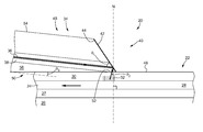
- FIG. 1 shows a schematic cross-sectional side view of an exemplary optical coupling assembly 20 according to an embodiment of the invention.
- the optical coupling assembly 20 first includes a planar waveguide 22 having a light-guiding path 24 .
- planar waveguide is understood to refer to an optical waveguide provided in a substantially integrated configuration, such as in a planar light circuit, and including a light guiding path supported by a suitable substrate. While the term “planar” suggests a flat structure, the term “planar waveguide” is also meant to encompass structures made of a plurality of flat layers.
- light-guiding path is understood to refer herein to a plane or an axis of a planar waveguide along which light can be guided.
- planar waveguide 22 may be embodied by any appropriate planar waveguide including, but not limited to, a slab waveguide, a strip waveguide, a ridge waveguide and a rib waveguide.
- the planar waveguide 22 may include a plurality of layers stacked on a substrate, one of these of layers defining the light-guiding path 24 .
- the planar waveguide 22 is a silicon-on-insulator (SOI) waveguide, that is, an integrated circuit based on SOI technology.
- SOI silicon-on-insulator
- the planar waveguide 22 therefore includes, successively, a substrate layer 26 , a lower cladding layer 27 and a core layer 28 defining the light-guiding path 24 .
- an optional upper cladding layer 30 may also be provided.
- other embodiments based on SOI technology may be provided without an upper cladding layer 30 disposed over the core layer 28 .
- SOI waveguides may be found, for instance, in U.S. Pat. No. 7,065,272 and U.S. Pat. No. 7,184,625 the contents of which are incorporated herein by reference. It is however understood that this structure is presented by way of example only and that different planar waveguide structures may be considered without departing from the scope of the present invention.
- the optical coupling assembly 20 according to embodiments of the present invention is not limited to SOI technology but may be based on various kinds of materials such as indium phosphide and gallium arsenide.
- the optical coupling assembly 20 also includes an optical fiber 34 having a light-guiding fiber core 36 surrounded by a fiber cladding 38 .
- the light-guiding fiber core 36 has preferably a refractive index higher than a refractive index of the fiber cladding 38 , so that light may be guided therealong.
- the optical fiber 34 may be made of plastic, glass, quartz, silica or the like. Additionally, the optical fiber 34 may be polarization maintaining.
- the optical fiber 34 has an angled tip 40 at one extremity thereof, the angled tip 40 making a cut angle ⁇ 1 with respect to the light-guiding fiber core 36 .
- the formation of the angled tip 40 of the optical fiber 34 may be achieved by polishing, cleaving, grinding, sawing, etching, focused-ion-beam (FIB) machining or laser machining one extremity of the optical fiber 34 at the selected cut angle ⁇ 1 .
- FIB focused-ion-beam
- the optical coupling assembly 20 further includes a reflective layer 42 provided on the angled tip 40 , thereby defining a reflection interface 44 , which is preferably substantially flat.
- the reflective layer 42 may for example be embodied by a metallic coating such as a gold, silver or aluminum coating. Alternatively, in other embodiments, the reflective layer 42 may be a dielectric coating.
- the reflective layer 42 may be deposited on the angled tip 40 using numerous techniques including, but not limited to, chemical vapor deposition (CVD), plasma-enhanced chemical vapor deposition (PECVD), ion beam deposition (evaporation coating), nanoscale growth, atomic layer deposition and molecular beam epitaxy.
- the reflective layer 42 need not cover the entire reflection interface 44 as long as it extends at least over the area on which light guided in the light-guiding fiber core 36 of the optical fiber 34 impinges. Accordingly, light traveling along the light-guiding fiber core 36 will be reflected by the reflection interface 44 regardless of whether or not the angle of incidence of light thereon exceeds the critical angle predicted by Snell's law for total internal reflection at the reflection interface 44 between the angled tip 40 and the surrounding medium.
- the optical coupling assembly 20 also includes a waveguide coupling element 32 for coupling light between the optical fiber 34 and the planar waveguide 22 .
- waveguide coupling element is understood to refer broadly to an optical element adapted for coupling light that is incident thereon from a given optical component (e.g. an optical fiber) into a waveguiding mode, and vice versa. More particularly, in the context of the coupling of light between an optical fiber and a planar waveguide, the term “waveguide coupling element” refers to an optical element capable of coupling a substantial fraction of an optical fiber mode into a waveguide mode, and vice versa.
- the waveguide coupling element 32 is a diffraction grating, which may include, within the planar waveguide 22 , linear corrugations or an embedded photonic crystal structure.
- diffraction grating may include, within the planar waveguide 22 , linear corrugations or an embedded photonic crystal structure.
- waveguide coupling element 32 is disposed in a region of the upper cladding 30 proximate to the core layer 28 in the embodiment of FIG. 1
- embodiments of the optical coupling assembly 20 are not limited by the location of the waveguide coupling element 32 within the planar waveguide 22 and various configurations are encompassed within the scope of the present invention.
- the waveguide coupling element 32 may be located completely inside the core layer 28 of the planar waveguide 22 , or partly inside the core layer 28 and one of the lower 27 and upper 30 cladding layers.
- the waveguide coupling element 32 may be provided integrally to the planar waveguide 22 , for example by inscribing the waveguide coupling element 32 within the material making up the planar waveguide 22 , or may be provided as an additional component.
- the term “light” is understood to refer to electromagnetic radiation in any appropriate region of electromagnetic spectrum and is not limited to visible light.
- the term “light” is meant to encompass electromagnetic radiation with a wavelength included in a range of between about 1520 nm to 1630 nm encompassing the C-band and L-band transmission windows for telecommunication applications, and of between about 1000 nm and 2000 nm for sensing applications.
- the optical fiber 34 extends along the planar waveguide 22 with the angled tip 40 positioned such that light propagating in the light-guiding fiber core 36 along a fiber propagation direction is reflected by the reflection interface 44 toward the waveguide coupling element 32 .
- the optical fiber 34 is positioned over the planar waveguide 22 so that the fiber cladding 38 is in direct contact with and extends contiguously from the planar waveguide 22 .
- the fiber cladding 38 and the planar waveguide 22 may be slightly spaced away from each other and may include therebetween a separation layer 45 .
- the separation layer 45 may include, without being limited to, an optically-transparent adhesive, a layer of an index-matching material, or air. It will be understood by one of ordinary skill in the art that the distance between the optical fiber 34 and the planar waveguide 22 should be minimized in order to maintain high optical power coupling efficiency therebetween.
- the optical fiber 34 is disposed over the planar waveguide 22 so as to ensure that the light-guiding fiber core 36 is parallel to the core layer 28 of the planar waveguide 22 .
- the light-guiding fiber core 36 and the core layer 28 may define a non-zero angle therebetween, as will be further described hereinbelow.
- the angle of incidence ⁇ 2 at which the light traveling along the light-guiding fiber core 36 is reflected by the reflection interface 44 toward the planar waveguide 22 depends on the cut angle ⁇ 1 and may be determined by the Snell's law which describes the behavior of light when moving between media of differing refractive indices, and by simple geometry.
- Equation (1) Upon inspection of Equation (1), one of ordinary skill in the art will understand that, in practice, the angle of incidence ⁇ 2 should be different from zero in order to avoid back-reflections due to Fresnel reflection and second-order Bragg diffraction at the top surface 46 of the planar waveguide 22 .
- the angled tip 40 of the optical fiber 34 extending along the planar waveguide 22 is positioned such that light reflected by the reflection interface 44 toward the waveguide coupling element 32 is coupled by the waveguide coupling element 32 to propagate in the light-guiding path 24 of the planar waveguide 22 along a waveguide propagation direction opposite to the fiber propagation direction.
- this condition implies that the angle of incidence ⁇ 2 , as defined above in Equation (1), should be negative. In the embodiment illustrated in FIG. 1 , this also implies that the cut angle ⁇ 1 of the angled tip 40 should therefore be greater than 45°.
- Equation (1) assumes that light reflected by the reflection interface 44 travels in straight line from the reflection interface 44 to the waveguide coupling element 32 , which, in the embodiment of FIG. 1 , will hold only if the fiber cladding 38 of the optical fiber 34 and the upper cladding layer 30 of the planar waveguide 22 have a same refractive index.
- the angle of incidence ⁇ 2 should be negative as measured in the vicinity of the waveguide coupling element 32 .
- an optical coupling assembly including a planar waveguide and an optical fiber component having, among other features, a tapered peripheral portion.
- FIGS. 2 to 5 there are shown schematic cross-sectional side views of exemplary optical coupling assemblies 20 according to embodiments of the invention.
- optical coupling assemblies 20 illustrated in FIGS. 2 to 5 share several common features with the optical coupling assembly 20 described above with reference to FIG. 1 . Therefore, the description of any common feature or variant thereof that were described above in relation to the embodiment shown in FIG. 1 will not be discussed in further detail hereinbelow.
- the optical coupling assembly 20 first includes a planar waveguide 22 having a light-guiding path 24 .
- the planar waveguide 22 may be embodied, for example, by a slab waveguide, a strip waveguide, a ridge waveguide and a rib waveguide.
- the planar waveguide 22 is a SOI waveguide and includes, successively, a substrate layer 26 , a lower cladding layer 27 and a core layer 28 defining the light-guiding path 24 .
- an optional upper cladding layer 30 may also be provided.
- other SOI waveguides 22 may be provided without an upper cladding layer 30 disposed over the core layer 28 .
- the optical coupling assembly 20 also includes an optical fiber component 48 , having a light-guiding fiber core 36 surrounded by a fiber cladding 38 .
- the optical fiber component 48 is simply an optical fiber 34 , as in the embodiment of FIG. 1 .
- the optical fiber component 48 may include additional structural elements, as will be discussed in further detail below with reference to the embodiment of FIG. 5 .
- the optical fiber component 48 also includes an angled tip 40 making a cut angle ⁇ 1 with respect to the light-guiding fiber core 36 and defining a reflection interface 44 .
- a reflective layer 42 may be provided on the angled tip 40 of the optical fiber 34 .
- the reflective layer 42 is optional and may be omitted if ⁇ 1 exceeds the critical angle predicted by Snell's law for total internal reflection at the reflection interface 44 the angled tip 40 and the surrounding medium.
- light propagating in the light-guiding fiber core 36 and impinging upon the reflection interface 44 may be reflected thereby by total internal reflection.
- the optical coupling assembly 20 further includes a waveguide coupling element 32 (e.g. a diffraction grating) for coupling light between the optical fiber 34 and the planar waveguide 22 .
- a waveguide coupling element 32 e.g. a diffraction grating
- the waveguide coupling element 28 is disposed in a region of the upper cladding proximate to the core layer 28 in the embodiment of FIG. 2
- embodiments of the optical coupling assembly 20 are not limited by the location of the waveguide coupling element 32 within the planar waveguide 22 and various configurations are encompassed within the scope of the present invention.
- the optical fiber component 48 of the embodiment of FIG. 2 also includes a tapered peripheral portion 50 tapering toward the angled tip 40 at a tapering angle ⁇ 3 .
- the tapering angle ⁇ 3 may be designed according to the geometry or configuration of the waveguide coupling element 32 provided with a particular planar waveguide 22 . Furthermore, depending on the intended application, the tapering angle ⁇ 3 may also be designed in order to minimize or maximize the contact surface between the optical fiber component 48 and the planar waveguide 22 .
- the cut angle ⁇ 1 of the angled tip 40 and the tapering angle ⁇ 3 of the tapered peripheral portion 50 may be jointly selected so that the light impinging on the reflection interface 44 and reflected thereby toward the waveguide coupling element 32 is incident on the waveguide coupling element 32 at an incidence angle ⁇ 2 of between about 5 and 20 degrees or between about ⁇ 5 and ⁇ 20 degrees with respect to the normal N to a plane of the planar waveguide 22 , that is, on either side of the normal N.
- a cut angle ⁇ 1 of 50° combined with a tapering angle ⁇ 3 of 6° together yield an incidence angle ⁇ 2 of ⁇ 16°.
- the waveguide coupling element 32 provided with the optical coupling assembly 20 illustrated in FIGS. 2 to 5 may couple light in the light-guiding path 24 of the planar waveguide 22 along a waveguide propagation direction that is either substantially the same (i.e. when ⁇ 2 >0) or opposite (i.e. when ⁇ 2 ⁇ 0) to a fiber propagation direction.
- FIG. 4 there is shown another optical coupling assembly 20 according to an embodiment of the invention, wherein light is coupled in the light-guiding 24 path of the planar waveguide 22 along a waveguide propagation direction substantially the same as the fiber propagation direction of light traveling along the light-guiding fiber core 36 of the optical fiber component 48 . More particularly, in this embodiment, the cut angle ⁇ 1 of 38° combined with the tapering angle ⁇ 3 of 6° together yield a positive incidence angle ⁇ 2 of 8°.
- the fiber cladding 38 of the optical fiber 34 preferably includes a tapered fiber cladding portion 52 defining at least part of the tapered peripheral portion 50 of the optical fiber component 48 .
- the tapered fiber cladding portion 52 defines completely the tapered peripheral portion 50 .
- the light-guiding fiber core 36 may include also a tapered fiber core portion defining part of the tapered peripheral portion 50 .
- the tapered peripheral portion 50 of the optical fiber component 48 is obtained by removing both a part of the fiber cladding 38 and a part of the light-guiding fiber core 36 .
- the optical fiber component 48 is disposed over the planar waveguide 22 with the tapered peripheral portion 50 extending therealong such that light propagating in the light-guiding fiber core 36 of the optical fiber component 48 along a fiber propagation direction is reflected by the reflection interface 44 toward the waveguide coupling element 32 and coupled thereby to propagate along a waveguide propagation direction in the light-guiding path 24 of the planar waveguide 22 .
- the tapered fiber cladding portion 52 which defines completely the tapered peripheral portion 50 of the optical fiber component 48 , is in direct contact with and extends contiguously from the cladding layer 30 of the planar waveguide 22 .
- the tapered fiber cladding portion 52 and the cladding layer 30 of the planar waveguide 22 may be slightly spaced away from each other and may include therebetween a separation layer 45 , for example an optically-transparent adhesive, a layer of an index-matching material, or air.
- optical coupling assemblies 20 of the embodiments illustrated in FIGS. 2 to 5 may be manufactured in a similar fashion than the optical coupling assemblies 20 of FIG. 1 , with an added step of removing a peripheral portion of the optical fiber component 48 by polishing, cleaving, grinding, sawing, etching, FIB machining laser machining or another appropriate means in order to define the tapered peripheral portion 50 of the optical fiber component 48 prior to disposing the same over the planar waveguide 22 .
- FIGS. 6B to 6D there are shown optical fibers provided with a tapered peripheral portion at a tapering angle of 6°, 4° and 2°.
- These tapered optical fibers illustrate advantages of the approach according to embodiments of the present invention over the prior art technique of defining a straight cut along the cladding of the fiber, which is exemplified in FIG. 6A (PRIOR ART).
- the straight cut of FIG. 6A (PRIOR ART) is difficult to produce and generally requires a complex apparatus since the removal of the fiber cladding must be very precise on a relatively long portion of the optical fiber along the axis thereof. This long portion is required to ensure a good contact between the optical fiber and the planar waveguide.
- an optical fiber with a tapered peripheral portion tapering at a tapering angle toward one extremity thereof may be performed with standard off-the-shelf polishing, grinding or dicing equipment and methods, so that no additional modification or complex equipment is required.
- the approach according to embodiments of the present invention involves no abrupt discontinuity in the thickness of the fiber cladding along the length of the optical fiber.
- the procedure is further simplified as only a limited portion of the fiber cladding needs to be polished or otherwise removed in FIGS. 6B to 6D , whereas in FIG. 6A (PRIOR ART), a portion of the fiber cladding must be removed along the whole length of the optical fiber to be disposed over the planar waveguide
- the tapered peripheral portion according to embodiments of the invention need not be fashioned directly into the fiber cladding of the optical fiber, as is the case for the embodiments of FIGS. 2 to 4 .
- FIG. 5 there is shown yet another embodiment of an optical coupling assembly 20 .
- the optical fiber component 48 further includes a fiber support 54 extending along the fiber cladding 38 proximate the angled tip 40 thereof.
- the fiber support 54 includes a tapered support portion 56 defining at least part of the tapered peripheral portion 50 .
- the fiber support 54 is an optical ferrule surrounding the fiber cladding, but other components may be used for supporting the optical fiber 34 , including a v-groove support or other appropriate holder.
- the optical ferrule 54 illustrated in FIG. 5 may be made of any appropriate material such as KovarTM, InvarTM, zirconia, borosilicate, silica or the like, and the optical fiber 34 may be assembled in the optical ferrule 54 by various attachment means such as soldering, glass solder, adhesive or mechanical crimping.
- the fiber support may be adapted to hold a plurality of optical fibers to be coupled on a given planar waveguide without departing from the scope of the present invention.
- the fiber support may be, for example, a multiple-hole optical ferrule, a v-groove array or a rectangular block having multiple holes bored therethrough.
- the optical coupling assembly 20 as exemplified in FIG. 5 may be manufactured by providing the fiber support 54 (e.g. optical ferrule) around one extremity of the optical fiber 34 and by performing two successive cuts to define the angled tip 40 and the tapered peripheral portion 50 of the optical fiber component 48 .
- the fiber support 54 e.g. optical ferrule
- a portion of the tapered peripheral portion 50 would then be cut along the fiber cladding 38 of the optical fiber 34 at one extremity thereof, thereby defining a tapered fiber cladding portion 52 .
- a fiber support such as an optical ferrule or a v-groove support for holding the optical fiber firmly while removing material from the extremity thereof would further ease the manufacturing process, and reduce the risk of chipping the extremity of the optical fiber while performing the two cuts.
Landscapes
- Physics & Mathematics (AREA)
- General Physics & Mathematics (AREA)
- Optics & Photonics (AREA)
- Optical Couplings Of Light Guides (AREA)
Abstract
Description
-
- a planar waveguide including a light-guiding path;
- an optical fiber including a light-guiding fiber core surrounded by a fiber cladding and having an angled tip;
- a reflective layer provided on the angled tip, thereby defining a reflection interface; and
- a waveguide coupling element for coupling light between the optical fiber and the planar waveguide,
- the optical fiber extending along the planar waveguide with the angled tip positioned such that light propagating in the light-guiding fiber core along a fiber propagation direction is reflected by the reflection interface toward the waveguide coupling element and coupled thereby to propagate in the light-guiding path of the waveguide along a waveguide propagation direction opposite to the fiber propagation direction.
-
- a planar waveguide including a light-guiding path;
- an optical fiber component including a light-guiding fiber core surrounded by a fiber cladding, an angled tip making a cut angle with respect to the light-guiding fiber core and defining a reflection interface, and a tapered peripheral portion tapering toward the angled tip at a tapering angle; and
- a waveguide coupling element for coupling light between the optical fiber component and the planar waveguide,
- the optical fiber component being disposed over the planar waveguide with the tapered peripheral portion extending therealong such that light propagating in the light-guiding fiber core of the optical fiber component is reflected by the reflection interface toward the waveguide coupling element and coupled thereby to propagate in the light-guiding path of the planar waveguide.
θ2=2×(45°−θ1)
θ2=2×(45°−θ1)−θ3
Claims (29)
Priority Applications (1)
| Application Number | Priority Date | Filing Date | Title |
|---|---|---|---|
| US13/550,325 US8639073B2 (en) | 2011-07-19 | 2012-07-16 | Fiber coupling technique on a waveguide |
Applications Claiming Priority (2)
| Application Number | Priority Date | Filing Date | Title |
|---|---|---|---|
| US201161509256P | 2011-07-19 | 2011-07-19 | |
| US13/550,325 US8639073B2 (en) | 2011-07-19 | 2012-07-16 | Fiber coupling technique on a waveguide |
Publications (2)
| Publication Number | Publication Date |
|---|---|
| US20130022316A1 US20130022316A1 (en) | 2013-01-24 |
| US8639073B2 true US8639073B2 (en) | 2014-01-28 |
Family
ID=47555817
Family Applications (1)
| Application Number | Title | Priority Date | Filing Date |
|---|---|---|---|
| US13/550,325 Active 2032-07-23 US8639073B2 (en) | 2011-07-19 | 2012-07-16 | Fiber coupling technique on a waveguide |
Country Status (1)
| Country | Link |
|---|---|
| US (1) | US8639073B2 (en) |
Cited By (13)
| Publication number | Priority date | Publication date | Assignee | Title |
|---|---|---|---|---|
| US20150021291A1 (en) * | 2013-07-18 | 2015-01-22 | Cisco Technology, Inc. | Coupling system for optical fibers and optical waveguides |
| US20150063745A1 (en) * | 2013-08-29 | 2015-03-05 | Industrial Technology Research Institute | Optical coupling module |
| US20150316718A1 (en) * | 2012-07-30 | 2015-11-05 | David A. Fattal | Optical coupling system and method for fabricating the same |
| US9274283B1 (en) * | 2014-09-30 | 2016-03-01 | Globalfoundries Inc. | Silicon photonics alignment tolerant vertical grating couplers |
| US9341786B1 (en) | 2015-07-28 | 2016-05-17 | Lumentum Operations Llc | Optomechanical assembly for a photonic chip |
| US9644966B2 (en) | 2014-09-11 | 2017-05-09 | Honeywell International Inc. | Integrated optic circuit with waveguides stitched at supplementary angles for reducing coherent backscatter |
| US9851521B2 (en) | 2014-07-07 | 2017-12-26 | Ciena Corporation | Connectorized optical chip assembly |
| US9941973B2 (en) | 2016-08-29 | 2018-04-10 | Ciena Corporation | Phase modulator with reduced residual amplitude modulation |
| US20180252876A1 (en) * | 2017-03-02 | 2018-09-06 | Sumitomo Electric Industries, Ltd. | Optical apparatus, stub device |
| US20190196114A1 (en) * | 2016-06-24 | 2019-06-27 | Senko Advanced Components (Hong Kong) Limited | A Parallel Optical Fiber Angled Coupling Component |
| US11112574B1 (en) | 2020-04-30 | 2021-09-07 | Hewlett Packard Enterprise Development Lp | Optoelectronic system with a wedge-shaped adapter |
| US11226504B2 (en) | 2019-07-19 | 2022-01-18 | Ciena Corporation | Free-carrier absorption variable optical attenuators and thermal phase shifters formed by an optical waveguide having multiple passes in an intrinsic region |
| US20220187544A1 (en) * | 2020-12-16 | 2022-06-16 | Md Elektronik Gmbh | Optical waveguide connector assembly |
Families Citing this family (34)
| Publication number | Priority date | Publication date | Assignee | Title |
|---|---|---|---|---|
| US10073264B2 (en) | 2007-08-03 | 2018-09-11 | Lumus Ltd. | Substrate-guide optical device |
| US10048499B2 (en) | 2005-11-08 | 2018-08-14 | Lumus Ltd. | Polarizing optical system |
| JP5376617B2 (en) * | 2011-09-13 | 2013-12-25 | 日立金属株式会社 | Photoelectric conversion module |
| US9091819B2 (en) * | 2013-04-11 | 2015-07-28 | International Business Machines Corporation | Grating edge coupler and method of forming same |
| JP6020329B2 (en) * | 2013-04-18 | 2016-11-02 | 日立金属株式会社 | Communication light detection structure, communication light detection optical connector and communication light detection optical cable having the same |
| EP2808713A1 (en) * | 2013-05-30 | 2014-12-03 | University College Cork - National University of Ireland, Cork | System and method for fiber packaging grating-coupled photonic devices |
| IL232197B (en) | 2014-04-23 | 2018-04-30 | Lumus Ltd | Compact head-mounted display system |
| US9453969B2 (en) * | 2014-04-29 | 2016-09-27 | Corning Optical Communications LLC | Grating-coupler assembly with small mode-field diameter for photonic-integrated-circuit systems |
| US9563018B2 (en) | 2014-10-09 | 2017-02-07 | International Business Machines Corporation | Tapered photonic waveguide to optical fiber proximity coupler |
| US9618698B2 (en) * | 2014-11-06 | 2017-04-11 | Huawei Technologies Co., Ltd. | Optical waveguide crossings |
| IL235642B (en) | 2014-11-11 | 2021-08-31 | Lumus Ltd | Compact head-mounted display system protected by a hyperfine structure |
| CN105242350B (en) * | 2015-10-27 | 2018-08-14 | 宁波屹诺电子科技有限公司 | A kind of silicon substrate plating metal speculum grating coupler and preparation method thereof |
| US10025033B2 (en) * | 2016-03-01 | 2018-07-17 | Advanced Semiconductor Engineering, Inc. | Optical fiber structure, optical communication apparatus and manufacturing process for manufacturing the same |
| CA2992213C (en) | 2016-10-09 | 2023-08-29 | Yochay Danziger | Aperture multiplier using a rectangular waveguide |
| KR20230084335A (en) * | 2016-11-08 | 2023-06-12 | 루머스 리미티드 | Light-guide device with optical cutoff edge and corresponding production methods |
| EP3397998A4 (en) | 2017-02-22 | 2019-04-17 | Lumus Ltd. | Light guide optical assembly |
| KR20230025946A (en) | 2017-03-22 | 2023-02-23 | 루머스 리미티드 | Overlapping facets |
| IL251645B (en) | 2017-04-06 | 2018-08-30 | Lumus Ltd | Light-guide optical element and method of its manufacture |
| JP2019003095A (en) * | 2017-06-16 | 2019-01-10 | 住友電気工業株式会社 | Optical component, optical device and manufacturing method of optical component |
| KR102537642B1 (en) | 2017-07-19 | 2023-05-26 | 루머스 리미티드 | LCOS lighting via LOE |
| US10551544B2 (en) | 2018-01-21 | 2020-02-04 | Lumus Ltd. | Light-guide optical element with multiple-axis internal aperture expansion |
| IL259518B2 (en) | 2018-05-22 | 2023-04-01 | Lumus Ltd | Optical system and method for improvement of light field uniformity |
| TWI813691B (en) | 2018-05-23 | 2023-09-01 | 以色列商魯姆斯有限公司 | Optical system including light-guide optical element with partially-reflective internal surfaces |
| US11415812B2 (en) | 2018-06-26 | 2022-08-16 | Lumus Ltd. | Compact collimating optical device and system |
| US10725244B2 (en) * | 2018-11-13 | 2020-07-28 | Institut National D'optique | Optical fiber with cladding-embedded light-converging structure for lateral optical coupling |
| US10677986B1 (en) | 2018-11-28 | 2020-06-09 | Ciena Corporation | Non-hermetic semiconductor optical amplifier integration on silicon photonics |
| JP7398131B2 (en) | 2019-03-12 | 2023-12-14 | ルムス エルティーディー. | image projector |
| CA3137994A1 (en) | 2019-06-27 | 2020-12-30 | Lumus Ltd | Apparatus and methods for eye tracking based on eye imaging via a light-guide optical element |
| KR20240059655A (en) | 2019-12-08 | 2024-05-07 | 루머스 리미티드 | Optical systems with compact image projector |
| CN116635773A (en) | 2021-03-01 | 2023-08-22 | 鲁姆斯有限公司 | Optical system with compact coupling from projector into waveguide |
| US11822088B2 (en) | 2021-05-19 | 2023-11-21 | Lumus Ltd. | Active optical engine |
| KR20230156802A (en) | 2021-07-04 | 2023-11-14 | 루머스 리미티드 | Display with stacked light guiding elements providing different parts of the field of view |
| TW202309570A (en) | 2021-08-23 | 2023-03-01 | 以色列商魯姆斯有限公司 | Methods of fabrication of compound light-guide optical elements having embedded coupling-in reflectors |
| WO2023229824A1 (en) * | 2022-05-27 | 2023-11-30 | Applied Materials, Inc. | Method to improve display efficiency and uniformity of ar waveguide |
Citations (10)
| Publication number | Priority date | Publication date | Assignee | Title |
|---|---|---|---|---|
| US5581639A (en) * | 1995-05-04 | 1996-12-03 | National Research Council Of Canada | Raman-nath diffraction grating |
| US7065272B2 (en) | 2002-04-10 | 2006-06-20 | Interuniversitair Microelektronica Centrum (Imec Vzw) | Fiber-to-waveguide coupler |
| US7162124B1 (en) | 2003-03-14 | 2007-01-09 | Luxtera, Inc. | Fiber to chip coupler |
| US7184625B2 (en) | 2003-02-11 | 2007-02-27 | Luxtera, Inc | Optical waveguide grating coupler incorporating reflective optical elements and anti-reflection elements |
| US20080002929A1 (en) * | 2006-06-30 | 2008-01-03 | Bowers John E | Electrically pumped semiconductor evanescent laser |
| US20090059988A1 (en) * | 2007-09-04 | 2009-03-05 | Fujitsu Limited | Semiconductor laser and semiconductor optical integrated device |
| US20100128576A1 (en) * | 2008-11-21 | 2010-05-27 | Fang Alexander W | Integrated magnetic recording head and near field laser |
| US8064745B2 (en) * | 2009-11-24 | 2011-11-22 | Corning Incorporated | Planar waveguide and optical fiber coupling |
| US20110299561A1 (en) * | 2009-03-05 | 2011-12-08 | Fujitsu Limited | Semiconductor laser silicon waveguide substrate, and integrated device |
| US20130215084A1 (en) * | 2010-02-08 | 2013-08-22 | Opdi Technologies A/S | Optical touch-sensitive device and method of detection of touch |
-
2012
- 2012-07-16 US US13/550,325 patent/US8639073B2/en active Active
Patent Citations (10)
| Publication number | Priority date | Publication date | Assignee | Title |
|---|---|---|---|---|
| US5581639A (en) * | 1995-05-04 | 1996-12-03 | National Research Council Of Canada | Raman-nath diffraction grating |
| US7065272B2 (en) | 2002-04-10 | 2006-06-20 | Interuniversitair Microelektronica Centrum (Imec Vzw) | Fiber-to-waveguide coupler |
| US7184625B2 (en) | 2003-02-11 | 2007-02-27 | Luxtera, Inc | Optical waveguide grating coupler incorporating reflective optical elements and anti-reflection elements |
| US7162124B1 (en) | 2003-03-14 | 2007-01-09 | Luxtera, Inc. | Fiber to chip coupler |
| US20080002929A1 (en) * | 2006-06-30 | 2008-01-03 | Bowers John E | Electrically pumped semiconductor evanescent laser |
| US20090059988A1 (en) * | 2007-09-04 | 2009-03-05 | Fujitsu Limited | Semiconductor laser and semiconductor optical integrated device |
| US20100128576A1 (en) * | 2008-11-21 | 2010-05-27 | Fang Alexander W | Integrated magnetic recording head and near field laser |
| US20110299561A1 (en) * | 2009-03-05 | 2011-12-08 | Fujitsu Limited | Semiconductor laser silicon waveguide substrate, and integrated device |
| US8064745B2 (en) * | 2009-11-24 | 2011-11-22 | Corning Incorporated | Planar waveguide and optical fiber coupling |
| US20130215084A1 (en) * | 2010-02-08 | 2013-08-22 | Opdi Technologies A/S | Optical touch-sensitive device and method of detection of touch |
Cited By (20)
| Publication number | Priority date | Publication date | Assignee | Title |
|---|---|---|---|---|
| US20150316718A1 (en) * | 2012-07-30 | 2015-11-05 | David A. Fattal | Optical coupling system and method for fabricating the same |
| US9568672B2 (en) * | 2012-07-30 | 2017-02-14 | Hewlett Packard Enterprise Development Lp | Optical coupling system and method for fabricating the same |
| US20150023631A1 (en) * | 2013-07-18 | 2015-01-22 | Cisco Technology, Inc | Coupling system for optical fibers and optical waveguides |
| US9122037B2 (en) * | 2013-07-18 | 2015-09-01 | Cisco Technology, Inc. | Coupling system for optical fibers and optical waveguides |
| US9134498B2 (en) * | 2013-07-18 | 2015-09-15 | Cisco Technology, Inc. | Coupling system for optical fibers and optical waveguides |
| US20150021291A1 (en) * | 2013-07-18 | 2015-01-22 | Cisco Technology, Inc. | Coupling system for optical fibers and optical waveguides |
| US9613886B2 (en) * | 2013-08-29 | 2017-04-04 | Industrial Technology Research Institute | Optical coupling module |
| US20150063745A1 (en) * | 2013-08-29 | 2015-03-05 | Industrial Technology Research Institute | Optical coupling module |
| US9851521B2 (en) | 2014-07-07 | 2017-12-26 | Ciena Corporation | Connectorized optical chip assembly |
| US9644966B2 (en) | 2014-09-11 | 2017-05-09 | Honeywell International Inc. | Integrated optic circuit with waveguides stitched at supplementary angles for reducing coherent backscatter |
| US9274283B1 (en) * | 2014-09-30 | 2016-03-01 | Globalfoundries Inc. | Silicon photonics alignment tolerant vertical grating couplers |
| US9341786B1 (en) | 2015-07-28 | 2016-05-17 | Lumentum Operations Llc | Optomechanical assembly for a photonic chip |
| US20190196114A1 (en) * | 2016-06-24 | 2019-06-27 | Senko Advanced Components (Hong Kong) Limited | A Parallel Optical Fiber Angled Coupling Component |
| US11415755B2 (en) * | 2016-06-24 | 2022-08-16 | Senko Advanced Components, Inc. | Parallel optical fiber angled coupling component |
| US9941973B2 (en) | 2016-08-29 | 2018-04-10 | Ciena Corporation | Phase modulator with reduced residual amplitude modulation |
| US20180252876A1 (en) * | 2017-03-02 | 2018-09-06 | Sumitomo Electric Industries, Ltd. | Optical apparatus, stub device |
| US11226504B2 (en) | 2019-07-19 | 2022-01-18 | Ciena Corporation | Free-carrier absorption variable optical attenuators and thermal phase shifters formed by an optical waveguide having multiple passes in an intrinsic region |
| US11112574B1 (en) | 2020-04-30 | 2021-09-07 | Hewlett Packard Enterprise Development Lp | Optoelectronic system with a wedge-shaped adapter |
| US20220187544A1 (en) * | 2020-12-16 | 2022-06-16 | Md Elektronik Gmbh | Optical waveguide connector assembly |
| US11592623B2 (en) * | 2020-12-16 | 2023-02-28 | Md Elektronik Gmbh | Optical waveguide connector assembly |
Also Published As
| Publication number | Publication date |
|---|---|
| US20130022316A1 (en) | 2013-01-24 |
Similar Documents
| Publication | Publication Date | Title |
|---|---|---|
| US8639073B2 (en) | Fiber coupling technique on a waveguide | |
| KR100277695B1 (en) | Method for manufacturing a substrate for hybrid optical integrated circuit using S-O optical waveguide | |
| US8503841B2 (en) | Device for coupling an optical fiber and a nanophotonic component | |
| EP3807686B1 (en) | Optical connectors and detachable optical connector assemblies for optical chips | |
| US8064745B2 (en) | Planar waveguide and optical fiber coupling | |
| US7162124B1 (en) | Fiber to chip coupler | |
| US4969712A (en) | Optoelectronic apparatus and method for its fabrication | |
| US7203390B2 (en) | Planar lightwave circuit package | |
| US9575257B2 (en) | Optical device, optical processing device, method for fabricating optical device | |
| CA3023857C (en) | Optical module | |
| KR100897887B1 (en) | Hybrid integration structure between optical active devices and planar lightwave circuit using fiber array | |
| KR100630804B1 (en) | Multi-wavelength optical tranceiver modules, multiplexer and demultiplexer using thin film filter | |
| JP2019003095A (en) | Optical component, optical device and manufacturing method of optical component | |
| EP0649038B1 (en) | Optical waveguide mirror | |
| US6892010B2 (en) | Photodetector/optical fiber apparatus with enhanced optical coupling efficiency and method for forming the same | |
| US6868210B2 (en) | Optical waveguide and their application of the optical communication system | |
| WO2004109354A1 (en) | Optical device | |
| US7260295B2 (en) | Optical waveguide and optical transmitting/receiving module | |
| WO2002031548A2 (en) | Optical component having a waveguide | |
| JP2000009953A (en) | Wavelength demultiplexer and optical transmission and reception module having the demultiplexer | |
| Rho et al. | WDM-PON module using a planar lightwave circuit with a coated WDM filter | |
| JPH0990146A (en) | Hybrid-type optical device and its manufacture | |
| JP2011090021A (en) | Method of assembling optical module | |
| JP2005134572A (en) | Optical waveguide circuit | |
| KR20070019137A (en) | Architecture of Optical WDM Filter on Planar Lightwave Circuit and Manufacturing Method thereof |
Legal Events
| Date | Code | Title | Description |
|---|---|---|---|
| AS | Assignment |
Owner name: TERAXION INC., CANADA Free format text: ASSIGNMENT OF ASSIGNORS INTEREST;ASSIGNORS:PELLETIER, FRANCOIS;ROBIDOUX, GUILLAUME;PAINCHAUD, YVES;SIGNING DATES FROM 20120808 TO 20120822;REEL/FRAME:028911/0039 |
|
| STCF | Information on status: patent grant |
Free format text: PATENTED CASE |
|
| AS | Assignment |
Owner name: CIENA CORPORATION, MARYLAND Free format text: ASSIGNMENT OF ASSIGNORS INTEREST;ASSIGNOR:CIENA CANADA, INC.;REEL/FRAME:038638/0214 Effective date: 20160505 Owner name: CIENA CANADA, INC., CANADA Free format text: ASSIGNMENT OF ASSIGNORS INTEREST;ASSIGNORS:TERAXION INC.;9333-9679 QUEBEC INC. (FORMERLY COGO OPTRONICS CANADA INC.);REEL/FRAME:038638/0153 Effective date: 20160201 |
|
| FEPP | Fee payment procedure |
Free format text: PAYOR NUMBER ASSIGNED (ORIGINAL EVENT CODE: ASPN); ENTITY STATUS OF PATENT OWNER: LARGE ENTITY Free format text: PAYER NUMBER DE-ASSIGNED (ORIGINAL EVENT CODE: RMPN); ENTITY STATUS OF PATENT OWNER: LARGE ENTITY |
|
| FEPP | Fee payment procedure |
Free format text: PAT HOLDER NO LONGER CLAIMS SMALL ENTITY STATUS, ENTITY STATUS SET TO UNDISCOUNTED (ORIGINAL EVENT CODE: STOL); ENTITY STATUS OF PATENT OWNER: LARGE ENTITY |
|
| FPAY | Fee payment |
Year of fee payment: 4 |
|
| AS | Assignment |
Owner name: CANADIAN IMPERIAL BANK OF COMMERCE, CANADA Free format text: SECURITY INTEREST;ASSIGNOR:TERAXION INC.;REEL/FRAME:050010/0398 Effective date: 20190729 |
|
| MAFP | Maintenance fee payment |
Free format text: PAYMENT OF MAINTENANCE FEE, 8TH YEAR, LARGE ENTITY (ORIGINAL EVENT CODE: M1552); ENTITY STATUS OF PATENT OWNER: LARGE ENTITY Year of fee payment: 8 |