US8438325B2 - Method and apparatus for improving small write performance in a non-volatile memory - Google Patents
Method and apparatus for improving small write performance in a non-volatile memory Download PDFInfo
- Publication number
- US8438325B2 US8438325B2 US12/248,690 US24869008A US8438325B2 US 8438325 B2 US8438325 B2 US 8438325B2 US 24869008 A US24869008 A US 24869008A US 8438325 B2 US8438325 B2 US 8438325B2
- Authority
- US
- United States
- Prior art keywords
- memory
- page
- reserve
- data
- block
- Prior art date
- Legal status (The legal status is an assumption and is not a legal conclusion. Google has not performed a legal analysis and makes no representation as to the accuracy of the status listed.)
- Expired - Fee Related, expires
Links
Images


Classifications
-
- G—PHYSICS
- G06—COMPUTING; CALCULATING OR COUNTING
- G06F—ELECTRIC DIGITAL DATA PROCESSING
- G06F12/00—Accessing, addressing or allocating within memory systems or architectures
- G06F12/02—Addressing or allocation; Relocation
- G06F12/0223—User address space allocation, e.g. contiguous or non contiguous base addressing
- G06F12/023—Free address space management
- G06F12/0238—Memory management in non-volatile memory, e.g. resistive RAM or ferroelectric memory
- G06F12/0246—Memory management in non-volatile memory, e.g. resistive RAM or ferroelectric memory in block erasable memory, e.g. flash memory
-
- G—PHYSICS
- G06—COMPUTING; CALCULATING OR COUNTING
- G06F—ELECTRIC DIGITAL DATA PROCESSING
- G06F2212/00—Indexing scheme relating to accessing, addressing or allocation within memory systems or architectures
- G06F2212/72—Details relating to flash memory management
- G06F2212/7202—Allocation control and policies
-
- G—PHYSICS
- G06—COMPUTING; CALCULATING OR COUNTING
- G06F—ELECTRIC DIGITAL DATA PROCESSING
- G06F2212/00—Indexing scheme relating to accessing, addressing or allocation within memory systems or architectures
- G06F2212/72—Details relating to flash memory management
- G06F2212/7203—Temporary buffering, e.g. using volatile buffer or dedicated buffer blocks
Definitions
- This invention relates generally to non-volatile memory, and more particularly to improving performance in block based non-volatile memory when performing random small write operations.
- Non-volatile memory is memory that stores data when power is disconnected from the system. Examples of non-volatile computer memory include Phase-change memory (PCM) and flash memory. Because non-volatile memory retains stored data even when power to the memory is turned off, non-volatile memory is widely used in battery-driven portable devices. For example, non-volatile memory often is utilized in digital audio players, digital cameras, mobile phones, and USB flash drives, which are used for general storage and transfer of data between computers.
- PCM Phase-change memory
- flash memory flash memory. Because non-volatile memory retains stored data even when power to the memory is turned off, non-volatile memory is widely used in battery-driven portable devices. For example, non-volatile memory often is utilized in digital audio players, digital cameras, mobile phones, and USB flash drives, which are used for general storage and transfer of data between computers.
- non-volatile memory systems are based on blocks of data to increase efficiency when handling large sequential streams of data.
- block based non-volatile memory systems often experience reduced efficiency when handling small and random write streams of data because unlike many other storage devices, non-volatile memory devices generally cannot be overwritten.
- the location must first be erased, then the new data written in its place.
- a memory block is the smallest element of data that can be erased in a block based non-volatile memory system.
- an entire block must be erased instead of just the particular page or pages of the block that were updated.
- non-volatile memory systems generally create an entirely new memory block having the updated data and remap the logical address of the old memory block to the new physical address of the block. Later, when time allows, the non-volatile memory system erases the old memory block containing the old data.
- FIG. 1A is a diagram showing a prior art non-volatile memory 100 .
- the non-volatile system 100 includes a plurality of memory blocks 102 , with each memory block comprising a plurality of memory pages 104 .
- the non-volatile memory controller locates a previously erased memory block, such as memory block 102 b , in which to store the data from page 104 a once updated.
- the data from memory page 104 a is transferred to the system data buffer, where the data is updated.
- the updated page data then is read from the system data buffer and written to the corresponding memory page 104 a ′ in the new memory block 102 b .
- the remainder of the memory pages from the original memory block 102 a are transferred to the new memory block 102 b , as illustrated next with reference to FIG. 1B .
- FIG. 1B is a diagram showing the prior art non-volatile memory 100 after transferring the remaining data in the original memory block 102 a to the new memory block 102 b .
- the non-volatile memory 100 includes a plurality of memory blocks 102 , with each memory block comprising a plurality of memory pages 104 .
- the update page data is written to the new memory page 102 b
- the data in the remainder of the memory pages 104 b of the original memory block 102 a needs to be transferred to the new memory block 102 b .
- FIG. 1B is a diagram showing the prior art non-volatile memory 100 after transferring the remaining data in the original memory block 102 a to the new memory block 102 b .
- the data is transferred from each old memory page 104 b to the corresponding new memory page 104 b ′ in the new memory block 102 b . Thereafter, when time permits, the original memory block 102 a can be erased.
- an exemplary memory block typically includes sixty-four memory pages
- the operations described above require: 1) 1 write of the new page data to the new page 104 a ′ in the new block 102 b, 2) 63 reads for the remaining pages in the original memory block 102 a , and 3) 63 writes of the pages to the new memory block 102 b .
- prior art memory systems generally require 127 page operations to update a single byte of data in a page of memory.
- the systems and methods should allow for effective use of memory, while improving memory performance.
- the systems and methods should reduce the amount of time required to perform small update operations by not requiring continuous read and write operations for each small random write operation.
- a method for performing write operation in non-volatile to target memory pages currently storing data.
- the method includes receiving a request to write update data to a target memory page located in a memory block when the memory page currently stores data.
- the request is processed by writing the update data to a reserve memory page located within the same memory block, thus avoiding an immediate need to copy all the pages of the memory block to a new memory block.
- a logical address associated with the physical address of the target memory page can be remapped to indicate the physical address of the reserve memory page.
- each memory block can be logically partitioned into user data memory pages and reserve memory pages.
- the user data memory pages generally are utilized to store user data
- each reserve memory page generally is utilized to store updated page data related to a particular user data memory page within the same memory block.
- the reserve memory pages in the memory block can have physical addresses near an end of a physical address range of the memory block, or dispersed throughout a physical address range of the memory block depending on the need and design of a particular system. It can sometimes occur that reserve memory pages may be unavailable at a particular time. In such cases, the update data can be written to a memory page of a new memory block when a free reserve memory page is currently unavailable in the memory block.
- multiple memory blocks are associated with a reserve memory block to improve performance during small write operations.
- the method includes associating a set of at least two memory blocks with a single reserve memory block, which comprises a plurality of reserve memory pages.
- the memory pages located within the set of memory blocks generally are user data memory pages used to store user data, while each reserve memory page is utilized to store updated page data related to a particular user data memory page within the set of memory blocks.
- a request to write update data to a target memory page is received, wherein the target memory page currently stores data and is located in one of the memory blocks of the set of memory blocks.
- the request is processed by writing the update data to a reserve memory page located in the reserve memory block. Once the update data is written to the reserve memory page, the logical address associated with the physical address of the target memory page can be remapped to indicate a physical address of the reserve memory page.
- a non-volatile memory that includes logical divisions to improve efficiency during small write operations.
- the memory pages of each memory block are logically divided into user data memory pages and reserve memory pages.
- data requested to be written to a target user data memory page in a memory block is written to a reserve memory page in the same memory block whenever the target user data memory page currently stores data, and reserve memory pages are currently available.
- the logical address associated with the physical address of the target memory page can be remapped to indicate a physical address of the reserve memory page.
- the logical address can be stored in a block table associated with the non-volatile memory and updated to indicate the actual physical address of the updated data.
- the logical address can be located within a spare area of the target user data memory page to indicate the actual physical address of the updated data.
- the logical address can be located in a spare area of the reserve memory page and can be mapped to indicate a physical address of the target user data memory page.
- FIG. 1A is a diagram showing a prior art non-volatile memory
- FIG. 1B is a diagram showing the prior art non-volatile memory after transferring remaining page data in the original memory block to a new memory block;
- FIG. 2 is a diagram showing an exemplary non-volatile memory block having reserve memory for small write operations, in accordance with an embodiment of the present invention
- FIG. 3 is a diagram showing an exemplary non-volatile memory block storing data from memory block in a continuous order, in accordance with an embodiment of the present invention
- FIG. 4 is a flowchart showing a method for improving performance during small write operates in a non-volatile memory, in accordance with an embodiment of the present invention.
- FIG. 5 is a diagram showing a plurality of associated memory blocks having a reserve memory block, in accordance with an embodiment of the present invention.
- An invention for improving performance in block based non-volatile memory when performing random small write operations.
- embodiments of the present invention improve performance by reserving memory pages for use during small write operations.
- the updated page data is written to a reserve memory page.
- the associated logical page address is temporarily remapped to the reserve page. Later, when time permits, the page data for the block can be reorganized into continuous pages in a new block.
- FIG. 2 is a diagram showing an exemplary non-volatile memory block 200 having reserve memory for small write operations, in accordance with an embodiment of the present invention.
- embodiments of the present invention reserve a plurality of memory pages, hereinafter termed reserve memory pages 204 , for use during small write operations.
- memory block 200 includes a plurality of user data memory pages 202 for use in storing user data and a plurality of reserve memory pages 204 for use in performing small write operates.
- the user data memory pages 202 and reserve memory pages 204 generally are physically the same type of memory pages utilized in non-volatile memory.
- embodiments of the present invention reserve a plurality of memory pages for use during small write operations.
- the number of pages reserved can vary depending on the particular needs of a system.
- the memory block 200 can include a total of 64 memory pages. Of these, 60 memory pages are utilized as user data memory pages 202 and four memory pages have been reserved as reserve memory pages 204 .
- any number of memory pages can be allocated as reserve memory pages 204 , for example, a memory block 200 can reserve two memory pages as reserve memory pages 204 , or if more pages are required, a particular system could reserve eight or more pages as reserve memory pages 204 .
- embodiments of the present invention allocate a predefined number of user data memory pages 202 for data and reserve a predefined number of reserve memory pages 204 for future small write updates. Then, when a request to perform a small write operation to a target memory page currently storing data, embodiments of the present invention perform the write operation to a reserve memory page 204 of the memory block 200 instead of allocating a new memory block and transferring all page data to the new block. The physical address of the selected reserve memory page 204 is then mapped to the logical address of the target memory page updated. Later, when time permits, the memory block can be reorganized to have continuous addressing.
- FIG. 2 memory block 200 includes pages 202 a and 202 b , which both currently store user data.
- the updated page data cannot be written directly to page 202 a because, in the example of FIG. 2 , page 202 a currently stores data.
- embodiments of the present invention determine whether a reserve memory page 204 is currently available in the memory block 200 . If a reserve memory page 204 is currently available, the updated page data is written to the available reserve memory page 204 and the logical address for page 202 a is updated to indicate the page data is now stored at the physical address of the reserve memory page.
- the updated page data for memory page 202 a is written to reserve memory page 204 a and the logical address of page 202 a is updated to indicate the page data is now stored at the physical address of memory page 204 a . If a second request to update page 202 a is received, the updated page data for memory page 202 a is written to reserve memory page 204 a ′ and the logical address of page 202 a is updated to indicate the page data is now stored at the physical address of memory page 204 a ′.
- the updated page data for memory page 202 b is written to reserve memory page 204 b and the logical address of page 202 b is updated to indicate the page data is now stored at the physical address of memory page 204 b.
- embodiments of the present invention can reorganize the memory block data when time permits, such as when the system is idle. For example, when time permits, a free memory block can be obtained and the data in the memory block 200 of FIG. 2 can be written to the free memory block in a continuous order, as illustrated in FIG. 3 .
- FIG. 3 is a diagram showing an exemplary non-volatile memory block 200 ′ storing data from memory block 200 in a continuous order, in accordance with an embodiment of the present invention.
- memory block 200 ′ includes a plurality of user data memory pages 202 for use in storing user data and a plurality of reserve memory pages 204 for use in performing small write operates.
- the reserve memory pages 204 of memory block 200 are written to appropriate physical addresses within the new memory block 200 ′. For example, the most up to date page data for memory page 202 a is stored in reserve memory page 204 a ′ in memory page 200 .
- the page data stored in reserve memory page 204 a ′ in memory block 200 is copied to page 202 a of the new memory block 200 ′, which corresponds to page 202 a of memory block 200 (i.e., has the same page address offset).
- the most up to date page data for memory page 202 b is stored in reserve memory page 204 b in memory block 200 .
- the page data stored in reserve memory page 204 b in memory block 200 is copied to page 202 b of the new memory block 200 ′, which corresponds to page 202 b of memory block 200 .
- the logical addresses corresponding to the memory pages 202 and 204 then are updated to indicate the corresponding pages in memory block 200 ′.
- FIG. 4 is a flowchart showing a method 400 for improving performance during small write operates in a non-volatile memory, in accordance with an embodiment of the present invention.
- preprocess operations are performed. Preprocess operations can include, for example, determining a number of memory pages to reserve in each memory block of non-volatile memory, updating data stored in non-volatile memory as requested by the system, and other preprocess operations that will be apparent to those skilled in the art after a careful reading of the present disclosure.
- a request is received to update data in a target memory page currently storing user data.
- a determination generally is made as to whether the target memory page currently stores data.
- the update data cannot be written directly to the target memory page due to limitations in the nature of non-volatile memory.
- embodiments of the present invention utilize available reserve memory pages to improve performance during the small write operation, as discussed below.
- the method 400 branches to operation 408 . Otherwise, the method 400 continues to operation 410 .
- a normal block update is performed in operation 408 .
- the non-volatile memory controller locates a new previously erased memory block in which to store the updated page data for the target page.
- the updated page data then is written to the corresponding memory page in the new memory block.
- the remaining memory pages from the original memory block are copied to corresponding memory pages of the new memory block. Thereafter, when time permits, the original memory block can be erased.
- the updated page data is written to an available reserve memory page, in operation 410 .
- the updated page data for target memory page 202 a is written to reserve memory page 204 a .
- the logical address for target memory page 202 a is updated to indicate the current page data for memory page 202 a is located at the physical address for reserve memory page 204 a.
- a plurality of methods can be utilized to determine whether a free reserve memory page is available and to remap the logical address of a target memory page to the physical address of the reserve memory page storing the updated page data. For example, in one embodiment page mapping is added to a block table residing in memory.
- the block table generally includes, among other data, data that indicates the mapping between logical addresses of user data and the actual physical addresses of user data.
- the block table In a block based system, the block table generally maps logical addresses of memory blocks to physical addresses of memory blocks within the non-volatile memory.
- page mapping data can indicate whether a particular memory page has been updated such that the current page data is stored in a reserve memory page.
- the page offset data can indicate whether a particular memory page has been updated such that the current page data is stored in a reserve memory page. For example, a page entry having a value of zero can indicate the related memory page has not been updated and the valid memory page is the original memory within the related memory block.
- a non-zero value for a page entry can indicate the offset to the particular reserve memory page within the memory block storing the current updated page data for the related memory page.
- Further embodiments can utilize a flag associate with each memory block in the block table.
- the flag can indicate whether a particular memory block includes current data stored in reserve memory pages, thus resulting in pages that are “out of order” with respect to the logical page addresses within the same memory block. This allows for faster processing of blocks that do not have “out of order” pages because subsequent address processing is not required for these pages.
- non-volatile memory pages often include a data area and a spare area.
- the data area is used to store user data within the memory page, while the spare area often is used to store error detection data, such as error correction codes (ECC) for the page.
- ECC error correction codes
- an offset to the original user data memory page can be included in the spare area of a reserve memory page if the reserve memory page stores updated page data for the original user data memory page.
- the spare areas of the reserve memory pages are examined to determine whether the reserve memory page stores valid data for a particular user data memory page in the memory block. If the reserve memory page stores valid data for a particular user data memory page, the offset data stored in the spare area of the reserve memory page indicates the offset to the original user data memory page related to the updated page data.
- Post process operations are performed in operation 412 .
- Post process operations can include updating related logical address to physical address mapping for the non-volatile memory, reordering of the page data during system idle periods, and other post process operations as will be apparent to those skilled in the art after a careful reading of the preset disclosure.
- the data for a memory block may no longer be in continuous addresses because of the use of the reserve memory pages.
- time permits such as when the system is idle, a free memory block can be obtained and the data in stored in the target memory block can be written to the free memory block in a continuous order.
- the reserve memory pages 204 of memory block 200 are written to appropriate physical addresses within the new memory block 200 ′.
- the most up to date page data for memory page 202 a is stored in reserve memory page 204 a ′ in memory page 200 .
- the page data stored in reserve memory page 204 a ′ in memory block 200 is copied to page 202 a of the new memory block 200 ′, which corresponds to page 202 a of memory block 200 .
- the page data stored in reserve memory page 204 b in memory block 200 is copied to page 202 b of the new memory block 200 ′, which corresponds to page 202 b of memory block 200 .
- the logical addresses corresponding to the memory pages 202 and 204 then are updated to indicate the corresponding pages in memory block 200 ′.
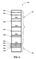
- FIG. 5 is a diagram showing a plurality of associated memory blocks 500 , in accordance with an embodiment of the present invention.
- the plurality of associated memory blocks 500 includes a plurality of user data memory blocks 502 and an associated reserve memory block 504 .
- Each user data memory block 502 includes a plurality of user data memory pages, similar to the user data memory pages of FIG. 2 .
- the user data memory blocks 502 generally do not include reserve memory pages, which generally are included in the reserve memory block 504 .
- the reserve memory block 504 generally includes only reserve memory pages.
- embodiments can be implemented that include reserve memory pages in user data memory blocks and user data memory pages in reserve memory blocks, depending on the needs of a particular system.
- embodiments of the present invention perform the write operation to a reserve memory page in the reserve memory block 504 associated with the user data memory block 502 including the target memory page.
- the physical address of the selected reserve memory page then is mapped to the logical address of the particular target memory page that was updated. Later, when time permits, the target memory block is reorganized to have continuous addressing.
- the exemplary associated memory blocks 500 of FIG. 5 include four user data memory blocks 502 a - 502 d associated with a reserve memory block 504 .
- FIG. 5 illustrates a memory block set 502 having four user data memory blocks, it should be noted that any number of user data memory blocks 500 can be associated with a reserve memory block 504 to form a set of associated memory blocks 500 .
- user data memory pages 506 a , 506 a ′, 506 b , 506 c , and 506 d all currently store user data, and as such cannot be directly overwritten with new data until erased.
- embodiments of the present invention determine whether a reserve memory page is currently available in the reserve memory block 504 . If a reserve memory page is currently available, the updated page data is written to the available reserve memory page and the logical address for page 506 a is updated to indicate the page data is now stored at the physical address of the selected reserve memory page in the reserve memory block.
- the updated page data for memory page 506 a in user data memory block 502 a is written to reserve memory page 508 a in the reserve memory block 504 and the logical address of page 506 a is updated to indicate the page data is now stored at the physical address of reserve memory page 508 a in the reserve memory block 504 .
- the updated page data for memory page 506 a ′ is written to reserve memory page 508 a ′ in the reserve memory block 504 and the logical address of page 506 a ′ is updated to indicate the page data is now stored at the physical address of memory page 508 a ′ in the reserve memory block 504 .
- the updated page data for memory page 506 b also is written to the reserve memory block 504 , at reserve memory page 508 b .
- an update to page 506 c is written to reserve memory page 508 c in the reserve memory block 504
- an update to page 506 d is written to reserve memory page 508 d in the reserve memory block 504
- an update to page 506 d is written to reserve memory page 508 d in the reserve memory block 504 .
- embodiments of the present invention reorganize the memory block data when time permits, such as when the system is idle. For example, when time permits, a free set of memory blocks can be obtained and the data in the user data memory blocks 502 of FIG. 5 written to the free memory blocks in a continuous order, substituting the updated page data in the reserve memory pages of the reserve memory block 504 for corresponding offset page addresses in the new memory block.
Abstract
Description
Claims (12)
Priority Applications (1)
| Application Number | Priority Date | Filing Date | Title |
|---|---|---|---|
| US12/248,690 US8438325B2 (en) | 2008-10-09 | 2008-10-09 | Method and apparatus for improving small write performance in a non-volatile memory |
Applications Claiming Priority (1)
| Application Number | Priority Date | Filing Date | Title |
|---|---|---|---|
| US12/248,690 US8438325B2 (en) | 2008-10-09 | 2008-10-09 | Method and apparatus for improving small write performance in a non-volatile memory |
Publications (2)
| Publication Number | Publication Date |
|---|---|
| US20100095046A1 US20100095046A1 (en) | 2010-04-15 |
| US8438325B2 true US8438325B2 (en) | 2013-05-07 |
Family
ID=42099925
Family Applications (1)
| Application Number | Title | Priority Date | Filing Date |
|---|---|---|---|
| US12/248,690 Expired - Fee Related US8438325B2 (en) | 2008-10-09 | 2008-10-09 | Method and apparatus for improving small write performance in a non-volatile memory |
Country Status (1)
| Country | Link |
|---|---|
| US (1) | US8438325B2 (en) |
Cited By (3)
| Publication number | Priority date | Publication date | Assignee | Title |
|---|---|---|---|---|
| US9606911B2 (en) * | 2010-05-24 | 2017-03-28 | Silicon Motion, Inc. | Apparatuses for managing and accessing flash memory module |
| US9886197B2 (en) | 2016-05-18 | 2018-02-06 | SK Hynix Inc. | Memory system and write and read operation method for the same |
| US11397545B1 (en) | 2021-01-20 | 2022-07-26 | Pure Storage, Inc. | Emulating persistent reservations in a cloud-based storage system |
Families Citing this family (9)
| Publication number | Priority date | Publication date | Assignee | Title |
|---|---|---|---|---|
| TWI514136B (en) * | 2010-12-28 | 2015-12-21 | Silicon Motion Inc | Flash memory device and data writing method thereof |
| US9152501B2 (en) | 2012-12-19 | 2015-10-06 | International Business Machines Corporation | Write performance in fault-tolerant clustered storage systems |
| US9678966B2 (en) * | 2013-11-08 | 2017-06-13 | Samsung Electronics Co., Ltd. | Swat command and API for atomic swap and trim of LBAs |
| US10068639B2 (en) | 2014-04-29 | 2018-09-04 | International Business Machines Corporation | Out-of-place presetting based on indirection table |
| WO2015196470A1 (en) * | 2014-06-27 | 2015-12-30 | 华为技术有限公司 | Method for writing data into flash memory device, flash memory device and storage system |
| TWI601141B (en) * | 2015-08-21 | 2017-10-01 | 晨星半導體股份有限公司 | Access method of flash memory and associated memory controller and electronic device |
| US11354420B2 (en) * | 2017-07-21 | 2022-06-07 | Red Hat, Inc. | Re-duplication of de-duplicated encrypted memory |
| KR20200089547A (en) * | 2019-01-17 | 2020-07-27 | 에스케이하이닉스 주식회사 | Storage device and operating method thereof |
| US11614956B2 (en) | 2019-12-06 | 2023-03-28 | Red Hat, Inc. | Multicast live migration for encrypted virtual machines |
Citations (10)
| Publication number | Priority date | Publication date | Assignee | Title |
|---|---|---|---|---|
| US20030101327A1 (en) * | 2001-11-16 | 2003-05-29 | Samsung Electronics Co., Ltd. | Flash memory management method |
| US20030165076A1 (en) * | 2001-09-28 | 2003-09-04 | Gorobets Sergey Anatolievich | Method of writing data to non-volatile memory |
| US20050144358A1 (en) * | 2003-12-30 | 2005-06-30 | Conley Kevin M. | Management of non-volatile memory systems having large erase blocks |
| US20060031627A1 (en) * | 2001-01-19 | 2006-02-09 | Conley Kevin M | Partial block data programming and reading operations in a non-volatile memory |
| US20070094440A1 (en) * | 2005-10-20 | 2007-04-26 | Simpletech, Inc. | Enhanced data access in a storage device |
| US20070245181A1 (en) * | 2005-09-29 | 2007-10-18 | Takaya Suda | Memory system and method of writing into nonvolatile semiconductor memory |
| US20080071970A1 (en) * | 2006-09-15 | 2008-03-20 | Lin Jason T | Non-Volatile Memory With Class-Based Update Block Replacement Rules |
| US20080189490A1 (en) * | 2007-02-06 | 2008-08-07 | Samsung Electronics Co., Ltd. | Memory mapping |
| US20090164705A1 (en) * | 2007-12-21 | 2009-06-25 | Gorobets Sergey A | System and Method for Implementing Extensions to Intelligently Manage Resources of a Mass Storage System |
| US20100095186A1 (en) * | 2008-08-20 | 2010-04-15 | Hanan Weingarten | Reprogramming non volatile memory portions |
-
2008
- 2008-10-09 US US12/248,690 patent/US8438325B2/en not_active Expired - Fee Related
Patent Citations (10)
| Publication number | Priority date | Publication date | Assignee | Title |
|---|---|---|---|---|
| US20060031627A1 (en) * | 2001-01-19 | 2006-02-09 | Conley Kevin M | Partial block data programming and reading operations in a non-volatile memory |
| US20030165076A1 (en) * | 2001-09-28 | 2003-09-04 | Gorobets Sergey Anatolievich | Method of writing data to non-volatile memory |
| US20030101327A1 (en) * | 2001-11-16 | 2003-05-29 | Samsung Electronics Co., Ltd. | Flash memory management method |
| US20050144358A1 (en) * | 2003-12-30 | 2005-06-30 | Conley Kevin M. | Management of non-volatile memory systems having large erase blocks |
| US20070245181A1 (en) * | 2005-09-29 | 2007-10-18 | Takaya Suda | Memory system and method of writing into nonvolatile semiconductor memory |
| US20070094440A1 (en) * | 2005-10-20 | 2007-04-26 | Simpletech, Inc. | Enhanced data access in a storage device |
| US20080071970A1 (en) * | 2006-09-15 | 2008-03-20 | Lin Jason T | Non-Volatile Memory With Class-Based Update Block Replacement Rules |
| US20080189490A1 (en) * | 2007-02-06 | 2008-08-07 | Samsung Electronics Co., Ltd. | Memory mapping |
| US20090164705A1 (en) * | 2007-12-21 | 2009-06-25 | Gorobets Sergey A | System and Method for Implementing Extensions to Intelligently Manage Resources of a Mass Storage System |
| US20100095186A1 (en) * | 2008-08-20 | 2010-04-15 | Hanan Weingarten | Reprogramming non volatile memory portions |
Non-Patent Citations (2)
| Title |
|---|
| Lee et al., A Log Buffer-Based Flash Translation Layer Using Fully-Associative Sector Translation, ACM Transactions on Embedded Computing Systems, Jul. 2007, vol. 6, No. 3, Article 18, pp. 18-es, US. |
| Lee et al., Last: Locality-Aware Sector Translation for NAND Flash Memory-Based Storage Systems, ACM Operating System Review, Oct. 2008, vol. 42, Issue 6, pp. 36-42, US. |
Cited By (4)
| Publication number | Priority date | Publication date | Assignee | Title |
|---|---|---|---|---|
| US9606911B2 (en) * | 2010-05-24 | 2017-03-28 | Silicon Motion, Inc. | Apparatuses for managing and accessing flash memory module |
| US9886197B2 (en) | 2016-05-18 | 2018-02-06 | SK Hynix Inc. | Memory system and write and read operation method for the same |
| US11397545B1 (en) | 2021-01-20 | 2022-07-26 | Pure Storage, Inc. | Emulating persistent reservations in a cloud-based storage system |
| US11693604B2 (en) | 2021-01-20 | 2023-07-04 | Pure Storage, Inc. | Administering storage access in a cloud-based storage system |
Also Published As
| Publication number | Publication date |
|---|---|
| US20100095046A1 (en) | 2010-04-15 |
Similar Documents
| Publication | Publication Date | Title |
|---|---|---|
| US8438325B2 (en) | Method and apparatus for improving small write performance in a non-volatile memory | |
| US10657047B2 (en) | Data storage device and method of performing partial garbage collection | |
| US9753847B2 (en) | Non-volatile semiconductor memory segregating sequential, random, and system data to reduce garbage collection for page based mapping | |
| US7814265B2 (en) | Single sector write operation in flash memory | |
| US8453021B2 (en) | Wear leveling in solid-state device | |
| US9529709B2 (en) | Apparatuses for managing and accessing flash memory module | |
| US8341371B2 (en) | Method of managing copy operations in flash memories | |
| US8180955B2 (en) | Computing systems and methods for managing flash memory device | |
| US11232041B2 (en) | Memory addressing | |
| US7844772B2 (en) | Device driver including a flash memory file system and method thereof and a flash memory device and method thereof | |
| US20080189490A1 (en) | Memory mapping | |
| US20080120488A1 (en) | Apparatus and method of managing nonvolatile memory | |
| US7287117B2 (en) | Flash memory and mapping control apparatus and method for flash memory | |
| US8521947B2 (en) | Method for writing data into flash memory | |
| US9122586B2 (en) | Physical-to-logical address map to speed up a recycle operation in a solid state drive | |
| US20140331024A1 (en) | Method of Dynamically Adjusting Mapping Manner in Non-Volatile Memory and Non-Volatile Storage Device Using the Same | |
| US7945762B2 (en) | Method and apparatus for memory management in a non-volatile memory system using a block table | |
| US7058784B2 (en) | Method for managing access operation on nonvolatile memory and block structure thereof | |
| US20050169058A1 (en) | Data management apparatus and method used for flash memory | |
| JP2012068765A (en) | Memory controller, flash memory system with memory controller, and control method of flash memory | |
| US20220164135A1 (en) | Apparatus, method and computer program for managing memory page updates within non-volatile memory | |
| JP2012037971A (en) | Memory controller, nonvolatile memory system provided with memory controller, and method for controlling nonvolatile memory |
Legal Events
| Date | Code | Title | Description |
|---|---|---|---|
| AS | Assignment |
Owner name: DENALI SOFTWARE, INC.,CALIFORNIA Free format text: ASSIGNMENT OF ASSIGNORS INTEREST;ASSIGNORS:REID, ROBERT ALAN;SHRADER, STEVEN L.;REEL/FRAME:021663/0117 Effective date: 20081002 Owner name: DENALI SOFTWARE, INC., CALIFORNIA Free format text: ASSIGNMENT OF ASSIGNORS INTEREST;ASSIGNORS:REID, ROBERT ALAN;SHRADER, STEVEN L.;REEL/FRAME:021663/0117 Effective date: 20081002 |
|
| AS | Assignment |
Owner name: CADENCE DESIGN SYSTEMS, INC, CALIFORNIA Free format text: ASSIGNMENT OF ASSIGNORS INTEREST;ASSIGNOR:NVELO, INC.;REEL/FRAME:026012/0094 Effective date: 20101027 |
|
| AS | Assignment |
Owner name: CADENCE DESIGN SYSTEMS, INC., CALIFORNIA Free format text: ASSIGNMENT OF ASSIGNORS INTEREST;ASSIGNOR:DENALI SOFTWARE, INC.;REEL/FRAME:026044/0090 Effective date: 20110328 |
|
| REMI | Maintenance fee reminder mailed | ||
| LAPS | Lapse for failure to pay maintenance fees | ||
| STCH | Information on status: patent discontinuation |
Free format text: PATENT EXPIRED DUE TO NONPAYMENT OF MAINTENANCE FEES UNDER 37 CFR 1.362 |
|
| FP | Lapsed due to failure to pay maintenance fee |
Effective date: 20170507 |