US8415200B2 - Method for manufacturing semiconductor package - Google Patents
Method for manufacturing semiconductor package Download PDFInfo
- Publication number
- US8415200B2 US8415200B2 US13/007,444 US201113007444A US8415200B2 US 8415200 B2 US8415200 B2 US 8415200B2 US 201113007444 A US201113007444 A US 201113007444A US 8415200 B2 US8415200 B2 US 8415200B2
- Authority
- US
- United States
- Prior art keywords
- layer
- metal
- metal layer
- semiconductor package
- manufacturing
- Prior art date
- Legal status (The legal status is an assumption and is not a legal conclusion. Google has not performed a legal analysis and makes no representation as to the accuracy of the status listed.)
- Expired - Fee Related
Links
- 238000000034 method Methods 0.000 title claims abstract description 65
- 239000004065 semiconductor Substances 0.000 title claims abstract description 61
- 238000004519 manufacturing process Methods 0.000 title claims abstract description 49
- 239000002184 metal Substances 0.000 claims abstract description 172
- 229910052751 metal Inorganic materials 0.000 claims abstract description 172
- 229910000679 solder Inorganic materials 0.000 claims abstract description 40
- 239000000853 adhesive Substances 0.000 claims abstract description 15
- 230000001070 adhesive effect Effects 0.000 claims abstract description 15
- 230000004888 barrier function Effects 0.000 claims abstract description 15
- 238000012545 processing Methods 0.000 claims abstract description 11
- 238000005530 etching Methods 0.000 claims description 39
- PXHVJJICTQNCMI-UHFFFAOYSA-N Nickel Chemical compound [Ni] PXHVJJICTQNCMI-UHFFFAOYSA-N 0.000 claims description 26
- 239000010949 copper Substances 0.000 claims description 20
- RYGMFSIKBFXOCR-UHFFFAOYSA-N Copper Chemical compound [Cu] RYGMFSIKBFXOCR-UHFFFAOYSA-N 0.000 claims description 18
- 229910052802 copper Inorganic materials 0.000 claims description 18
- 229910052759 nickel Inorganic materials 0.000 claims description 12
- 238000000059 patterning Methods 0.000 claims description 12
- 238000010030 laminating Methods 0.000 claims description 6
- 239000010410 layer Substances 0.000 abstract description 166
- 238000007747 plating Methods 0.000 abstract description 9
- 239000011229 interlayer Substances 0.000 abstract description 4
- 239000000758 substrate Substances 0.000 abstract description 2
- 229920005989 resin Polymers 0.000 description 4
- 239000011347 resin Substances 0.000 description 4
- 230000008901 benefit Effects 0.000 description 3
- 239000000126 substance Substances 0.000 description 3
- 239000004593 Epoxy Substances 0.000 description 2
- 238000007792 addition Methods 0.000 description 2
- 238000005553 drilling Methods 0.000 description 2
- 230000000694 effects Effects 0.000 description 2
- 238000005516 engineering process Methods 0.000 description 2
- 238000012986 modification Methods 0.000 description 2
- 230000004048 modification Effects 0.000 description 2
- 238000005498 polishing Methods 0.000 description 2
- 239000002952 polymeric resin Substances 0.000 description 2
- 238000006467 substitution reaction Methods 0.000 description 2
- 229920003002 synthetic resin Polymers 0.000 description 2
- 239000002253 acid Substances 0.000 description 1
- 239000000919 ceramic Substances 0.000 description 1
- 238000011161 development Methods 0.000 description 1
- 239000000463 material Substances 0.000 description 1
- 238000012536 packaging technology Methods 0.000 description 1
- 238000002203 pretreatment Methods 0.000 description 1
- 238000011160 research Methods 0.000 description 1
- 238000005201 scrubbing Methods 0.000 description 1
Images


Classifications
-
- H—ELECTRICITY
- H01—ELECTRIC ELEMENTS
- H01L—SEMICONDUCTOR DEVICES NOT COVERED BY CLASS H10
- H01L23/00—Details of semiconductor or other solid state devices
- H01L23/48—Arrangements for conducting electric current to or from the solid state body in operation, e.g. leads, terminal arrangements ; Selection of materials therefor
- H01L23/488—Arrangements for conducting electric current to or from the solid state body in operation, e.g. leads, terminal arrangements ; Selection of materials therefor consisting of soldered or bonded constructions
- H01L23/498—Leads, i.e. metallisations or lead-frames on insulating substrates, e.g. chip carriers
- H01L23/49827—Via connections through the substrates, e.g. pins going through the substrate, coaxial cables
-
- H—ELECTRICITY
- H01—ELECTRIC ELEMENTS
- H01L—SEMICONDUCTOR DEVICES NOT COVERED BY CLASS H10
- H01L21/00—Processes or apparatus adapted for the manufacture or treatment of semiconductor or solid state devices or of parts thereof
- H01L21/02—Manufacture or treatment of semiconductor devices or of parts thereof
- H01L21/04—Manufacture or treatment of semiconductor devices or of parts thereof the devices having potential barriers, e.g. a PN junction, depletion layer or carrier concentration layer
- H01L21/48—Manufacture or treatment of parts, e.g. containers, prior to assembly of the devices, using processes not provided for in a single one of the subgroups H01L21/06 - H01L21/326
- H01L21/4814—Conductive parts
- H01L21/4846—Leads on or in insulating or insulated substrates, e.g. metallisation
- H01L21/486—Via connections through the substrate with or without pins
-
- H—ELECTRICITY
- H01—ELECTRIC ELEMENTS
- H01L—SEMICONDUCTOR DEVICES NOT COVERED BY CLASS H10
- H01L23/00—Details of semiconductor or other solid state devices
- H01L23/48—Arrangements for conducting electric current to or from the solid state body in operation, e.g. leads, terminal arrangements ; Selection of materials therefor
- H01L23/488—Arrangements for conducting electric current to or from the solid state body in operation, e.g. leads, terminal arrangements ; Selection of materials therefor consisting of soldered or bonded constructions
- H01L23/498—Leads, i.e. metallisations or lead-frames on insulating substrates, e.g. chip carriers
- H01L23/49866—Leads, i.e. metallisations or lead-frames on insulating substrates, e.g. chip carriers characterised by the materials
- H01L23/49894—Materials of the insulating layers or coatings
-
- H—ELECTRICITY
- H05—ELECTRIC TECHNIQUES NOT OTHERWISE PROVIDED FOR
- H05K—PRINTED CIRCUITS; CASINGS OR CONSTRUCTIONAL DETAILS OF ELECTRIC APPARATUS; MANUFACTURE OF ASSEMBLAGES OF ELECTRICAL COMPONENTS
- H05K3/00—Apparatus or processes for manufacturing printed circuits
- H05K3/40—Forming printed elements for providing electric connections to or between printed circuits
- H05K3/4038—Through-connections; Vertical interconnect access [VIA] connections
-
- H—ELECTRICITY
- H01—ELECTRIC ELEMENTS
- H01L—SEMICONDUCTOR DEVICES NOT COVERED BY CLASS H10
- H01L2224/00—Indexing scheme for arrangements for connecting or disconnecting semiconductor or solid-state bodies and methods related thereto as covered by H01L24/00
- H01L2224/01—Means for bonding being attached to, or being formed on, the surface to be connected, e.g. chip-to-package, die-attach, "first-level" interconnects; Manufacturing methods related thereto
- H01L2224/10—Bump connectors; Manufacturing methods related thereto
- H01L2224/12—Structure, shape, material or disposition of the bump connectors prior to the connecting process
- H01L2224/13—Structure, shape, material or disposition of the bump connectors prior to the connecting process of an individual bump connector
- H01L2224/13001—Core members of the bump connector
- H01L2224/13099—Material
- H01L2224/131—Material with a principal constituent of the material being a metal or a metalloid, e.g. boron [B], silicon [Si], germanium [Ge], arsenic [As], antimony [Sb], tellurium [Te] and polonium [Po], and alloys thereof
-
- H—ELECTRICITY
- H01—ELECTRIC ELEMENTS
- H01L—SEMICONDUCTOR DEVICES NOT COVERED BY CLASS H10
- H01L2224/00—Indexing scheme for arrangements for connecting or disconnecting semiconductor or solid-state bodies and methods related thereto as covered by H01L24/00
- H01L2224/01—Means for bonding being attached to, or being formed on, the surface to be connected, e.g. chip-to-package, die-attach, "first-level" interconnects; Manufacturing methods related thereto
- H01L2224/10—Bump connectors; Manufacturing methods related thereto
- H01L2224/15—Structure, shape, material or disposition of the bump connectors after the connecting process
- H01L2224/16—Structure, shape, material or disposition of the bump connectors after the connecting process of an individual bump connector
- H01L2224/161—Disposition
- H01L2224/16151—Disposition the bump connector connecting between a semiconductor or solid-state body and an item not being a semiconductor or solid-state body, e.g. chip-to-substrate, chip-to-passive
- H01L2224/16221—Disposition the bump connector connecting between a semiconductor or solid-state body and an item not being a semiconductor or solid-state body, e.g. chip-to-substrate, chip-to-passive the body and the item being stacked
- H01L2224/16225—Disposition the bump connector connecting between a semiconductor or solid-state body and an item not being a semiconductor or solid-state body, e.g. chip-to-substrate, chip-to-passive the body and the item being stacked the item being non-metallic, e.g. insulating substrate with or without metallisation
- H01L2224/16237—Disposition the bump connector connecting between a semiconductor or solid-state body and an item not being a semiconductor or solid-state body, e.g. chip-to-substrate, chip-to-passive the body and the item being stacked the item being non-metallic, e.g. insulating substrate with or without metallisation the bump connector connecting to a bonding area disposed in a recess of the surface of the item
-
- H—ELECTRICITY
- H01—ELECTRIC ELEMENTS
- H01L—SEMICONDUCTOR DEVICES NOT COVERED BY CLASS H10
- H01L2224/00—Indexing scheme for arrangements for connecting or disconnecting semiconductor or solid-state bodies and methods related thereto as covered by H01L24/00
- H01L2224/01—Means for bonding being attached to, or being formed on, the surface to be connected, e.g. chip-to-package, die-attach, "first-level" interconnects; Manufacturing methods related thereto
- H01L2224/42—Wire connectors; Manufacturing methods related thereto
- H01L2224/47—Structure, shape, material or disposition of the wire connectors after the connecting process
- H01L2224/48—Structure, shape, material or disposition of the wire connectors after the connecting process of an individual wire connector
- H01L2224/4805—Shape
- H01L2224/4809—Loop shape
- H01L2224/48091—Arched
-
- H—ELECTRICITY
- H01—ELECTRIC ELEMENTS
- H01L—SEMICONDUCTOR DEVICES NOT COVERED BY CLASS H10
- H01L2224/00—Indexing scheme for arrangements for connecting or disconnecting semiconductor or solid-state bodies and methods related thereto as covered by H01L24/00
- H01L2224/01—Means for bonding being attached to, or being formed on, the surface to be connected, e.g. chip-to-package, die-attach, "first-level" interconnects; Manufacturing methods related thereto
- H01L2224/42—Wire connectors; Manufacturing methods related thereto
- H01L2224/47—Structure, shape, material or disposition of the wire connectors after the connecting process
- H01L2224/48—Structure, shape, material or disposition of the wire connectors after the connecting process of an individual wire connector
- H01L2224/481—Disposition
- H01L2224/48151—Connecting between a semiconductor or solid-state body and an item not being a semiconductor or solid-state body, e.g. chip-to-substrate, chip-to-passive
- H01L2224/48221—Connecting between a semiconductor or solid-state body and an item not being a semiconductor or solid-state body, e.g. chip-to-substrate, chip-to-passive the body and the item being stacked
- H01L2224/48225—Connecting between a semiconductor or solid-state body and an item not being a semiconductor or solid-state body, e.g. chip-to-substrate, chip-to-passive the body and the item being stacked the item being non-metallic, e.g. insulating substrate with or without metallisation
- H01L2224/4824—Connecting between the body and an opposite side of the item with respect to the body
-
- H—ELECTRICITY
- H01—ELECTRIC ELEMENTS
- H01L—SEMICONDUCTOR DEVICES NOT COVERED BY CLASS H10
- H01L2224/00—Indexing scheme for arrangements for connecting or disconnecting semiconductor or solid-state bodies and methods related thereto as covered by H01L24/00
- H01L2224/73—Means for bonding being of different types provided for in two or more of groups H01L2224/10, H01L2224/18, H01L2224/26, H01L2224/34, H01L2224/42, H01L2224/50, H01L2224/63, H01L2224/71
- H01L2224/732—Location after the connecting process
- H01L2224/73201—Location after the connecting process on the same surface
- H01L2224/73215—Layer and wire connectors
-
- H—ELECTRICITY
- H01—ELECTRIC ELEMENTS
- H01L—SEMICONDUCTOR DEVICES NOT COVERED BY CLASS H10
- H01L2224/00—Indexing scheme for arrangements for connecting or disconnecting semiconductor or solid-state bodies and methods related thereto as covered by H01L24/00
- H01L2224/80—Methods for connecting semiconductor or other solid state bodies using means for bonding being attached to, or being formed on, the surface to be connected
- H01L2224/81—Methods for connecting semiconductor or other solid state bodies using means for bonding being attached to, or being formed on, the surface to be connected using a bump connector
- H01L2224/8119—Arrangement of the bump connectors prior to mounting
- H01L2224/81192—Arrangement of the bump connectors prior to mounting wherein the bump connectors are disposed only on another item or body to be connected to the semiconductor or solid-state body
-
- H—ELECTRICITY
- H01—ELECTRIC ELEMENTS
- H01L—SEMICONDUCTOR DEVICES NOT COVERED BY CLASS H10
- H01L2224/00—Indexing scheme for arrangements for connecting or disconnecting semiconductor or solid-state bodies and methods related thereto as covered by H01L24/00
- H01L2224/80—Methods for connecting semiconductor or other solid state bodies using means for bonding being attached to, or being formed on, the surface to be connected
- H01L2224/81—Methods for connecting semiconductor or other solid state bodies using means for bonding being attached to, or being formed on, the surface to be connected using a bump connector
- H01L2224/8138—Bonding interfaces outside the semiconductor or solid-state body
- H01L2224/81385—Shape, e.g. interlocking features
-
- H—ELECTRICITY
- H01—ELECTRIC ELEMENTS
- H01L—SEMICONDUCTOR DEVICES NOT COVERED BY CLASS H10
- H01L2224/00—Indexing scheme for arrangements for connecting or disconnecting semiconductor or solid-state bodies and methods related thereto as covered by H01L24/00
- H01L2224/80—Methods for connecting semiconductor or other solid state bodies using means for bonding being attached to, or being formed on, the surface to be connected
- H01L2224/81—Methods for connecting semiconductor or other solid state bodies using means for bonding being attached to, or being formed on, the surface to be connected using a bump connector
- H01L2224/818—Bonding techniques
- H01L2224/81801—Soldering or alloying
- H01L2224/81815—Reflow soldering
-
- H—ELECTRICITY
- H01—ELECTRIC ELEMENTS
- H01L—SEMICONDUCTOR DEVICES NOT COVERED BY CLASS H10
- H01L23/00—Details of semiconductor or other solid state devices
- H01L23/48—Arrangements for conducting electric current to or from the solid state body in operation, e.g. leads, terminal arrangements ; Selection of materials therefor
- H01L23/488—Arrangements for conducting electric current to or from the solid state body in operation, e.g. leads, terminal arrangements ; Selection of materials therefor consisting of soldered or bonded constructions
- H01L23/498—Leads, i.e. metallisations or lead-frames on insulating substrates, e.g. chip carriers
- H01L23/49811—Additional leads joined to the metallisation on the insulating substrate, e.g. pins, bumps, wires, flat leads
- H01L23/49816—Spherical bumps on the substrate for external connection, e.g. ball grid arrays [BGA]
-
- H—ELECTRICITY
- H01—ELECTRIC ELEMENTS
- H01L—SEMICONDUCTOR DEVICES NOT COVERED BY CLASS H10
- H01L24/00—Arrangements for connecting or disconnecting semiconductor or solid-state bodies; Methods or apparatus related thereto
- H01L24/01—Means for bonding being attached to, or being formed on, the surface to be connected, e.g. chip-to-package, die-attach, "first-level" interconnects; Manufacturing methods related thereto
- H01L24/10—Bump connectors ; Manufacturing methods related thereto
- H01L24/15—Structure, shape, material or disposition of the bump connectors after the connecting process
- H01L24/16—Structure, shape, material or disposition of the bump connectors after the connecting process of an individual bump connector
-
- H—ELECTRICITY
- H01—ELECTRIC ELEMENTS
- H01L—SEMICONDUCTOR DEVICES NOT COVERED BY CLASS H10
- H01L24/00—Arrangements for connecting or disconnecting semiconductor or solid-state bodies; Methods or apparatus related thereto
- H01L24/01—Means for bonding being attached to, or being formed on, the surface to be connected, e.g. chip-to-package, die-attach, "first-level" interconnects; Manufacturing methods related thereto
- H01L24/42—Wire connectors; Manufacturing methods related thereto
- H01L24/47—Structure, shape, material or disposition of the wire connectors after the connecting process
- H01L24/48—Structure, shape, material or disposition of the wire connectors after the connecting process of an individual wire connector
-
- H—ELECTRICITY
- H01—ELECTRIC ELEMENTS
- H01L—SEMICONDUCTOR DEVICES NOT COVERED BY CLASS H10
- H01L24/00—Arrangements for connecting or disconnecting semiconductor or solid-state bodies; Methods or apparatus related thereto
- H01L24/80—Methods for connecting semiconductor or other solid state bodies using means for bonding being attached to, or being formed on, the surface to be connected
- H01L24/81—Methods for connecting semiconductor or other solid state bodies using means for bonding being attached to, or being formed on, the surface to be connected using a bump connector
-
- H—ELECTRICITY
- H01—ELECTRIC ELEMENTS
- H01L—SEMICONDUCTOR DEVICES NOT COVERED BY CLASS H10
- H01L2924/00—Indexing scheme for arrangements or methods for connecting or disconnecting semiconductor or solid-state bodies as covered by H01L24/00
- H01L2924/0001—Technical content checked by a classifier
- H01L2924/00014—Technical content checked by a classifier the subject-matter covered by the group, the symbol of which is combined with the symbol of this group, being disclosed without further technical details
-
- H—ELECTRICITY
- H01—ELECTRIC ELEMENTS
- H01L—SEMICONDUCTOR DEVICES NOT COVERED BY CLASS H10
- H01L2924/00—Indexing scheme for arrangements or methods for connecting or disconnecting semiconductor or solid-state bodies as covered by H01L24/00
- H01L2924/01—Chemical elements
- H01L2924/01087—Francium [Fr]
-
- H—ELECTRICITY
- H01—ELECTRIC ELEMENTS
- H01L—SEMICONDUCTOR DEVICES NOT COVERED BY CLASS H10
- H01L2924/00—Indexing scheme for arrangements or methods for connecting or disconnecting semiconductor or solid-state bodies as covered by H01L24/00
- H01L2924/15—Details of package parts other than the semiconductor or other solid state devices to be connected
- H01L2924/151—Die mounting substrate
- H01L2924/153—Connection portion
- H01L2924/1531—Connection portion the connection portion being formed only on the surface of the substrate opposite to the die mounting surface
- H01L2924/15311—Connection portion the connection portion being formed only on the surface of the substrate opposite to the die mounting surface being a ball array, e.g. BGA
-
- H—ELECTRICITY
- H05—ELECTRIC TECHNIQUES NOT OTHERWISE PROVIDED FOR
- H05K—PRINTED CIRCUITS; CASINGS OR CONSTRUCTIONAL DETAILS OF ELECTRIC APPARATUS; MANUFACTURE OF ASSEMBLAGES OF ELECTRICAL COMPONENTS
- H05K2203/00—Indexing scheme relating to apparatus or processes for manufacturing printed circuits covered by H05K3/00
- H05K2203/03—Metal processing
- H05K2203/0384—Etch stop layer, i.e. a buried barrier layer for preventing etching of layers under the etch stop layer
-
- H—ELECTRICITY
- H05—ELECTRIC TECHNIQUES NOT OTHERWISE PROVIDED FOR
- H05K—PRINTED CIRCUITS; CASINGS OR CONSTRUCTIONAL DETAILS OF ELECTRIC APPARATUS; MANUFACTURE OF ASSEMBLAGES OF ELECTRICAL COMPONENTS
- H05K3/00—Apparatus or processes for manufacturing printed circuits
- H05K3/02—Apparatus or processes for manufacturing printed circuits in which the conductive material is applied to the surface of the insulating support and is thereafter removed from such areas of the surface which are not intended for current conducting or shielding
- H05K3/06—Apparatus or processes for manufacturing printed circuits in which the conductive material is applied to the surface of the insulating support and is thereafter removed from such areas of the surface which are not intended for current conducting or shielding the conductive material being removed chemically or electrolytically, e.g. by photo-etch process
-
- H—ELECTRICITY
- H05—ELECTRIC TECHNIQUES NOT OTHERWISE PROVIDED FOR
- H05K—PRINTED CIRCUITS; CASINGS OR CONSTRUCTIONAL DETAILS OF ELECTRIC APPARATUS; MANUFACTURE OF ASSEMBLAGES OF ELECTRICAL COMPONENTS
- H05K3/00—Apparatus or processes for manufacturing printed circuits
- H05K3/46—Manufacturing multilayer circuits
- H05K3/4644—Manufacturing multilayer circuits by building the multilayer layer by layer, i.e. build-up multilayer circuits
- H05K3/4647—Manufacturing multilayer circuits by building the multilayer layer by layer, i.e. build-up multilayer circuits by applying an insulating layer around previously made via studs
Definitions
- the present invention relates to a method for manufacturing a semiconductor package.
- the semiconductor package may be designed only with a printed circuit board that includes only a single metal layer, and as a result, is in a superior position in terms of price competitiveness of a semiconductor package.
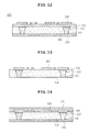
- FIGS. 1 to 6 are cross-sectional views showing a method for manufacturing a semiconductor package according to the prior art in a process sequence.
- a copper clad laminate configured of an insulating layer 1 and a copper layer 2 is provided and a through hole 3 is machined on the copper clad laminate for interlayer conduction.
- the through hole is generally formed using CNC drilling or laser drilling.
- a chemical copper plating process and an electrical copper plating process are performed, thereby forming a copper plating layer 4 over the copper clad laminate.
- the inside of the through hole 3 is filled with a plugging ink 5 and a plating is performed on the panel, thereby forming a plating layer 6 that is to be thick.
- the plating layer 6 is selectively etched, thereby forming a circuit pattern 7 .
- a solder resist 8 is applied to both surfaces of the copper clad laminate formed with the circuit pattern 7 and an opening part is formed so that a portion of the circuit pattern 7 is opened.
- a solder ball 10 is formed on a pad part of the circuit pattern 7 and a semiconductor chip 20 is mounted on the substrate using the wire 30 , thereby implementing a semiconductor package 50 .
- the through hole should be formed on the copper clad laminate for interlayer conduction and the electrical/chemical copper plating processes should also be performed, which causes increase in manufacturing costs.
- the present invention has been made in an effort to provide a method for manufacturing a semiconductor package capable of being implemented in a high-density package at low manufacturing costs.
- a method for manufacturing a semiconductor package including: (A) preparing a metal member in which a first metal layer, a barrier layer, and a second metal layer are stacked in sequence; (B) forming a metal post by selectively etching the second metal layer; (C) removing the exposed bather layer from the metal post and laminating an insulating layer on the first metal layer through which the metal post is penetrated; and (D) patterning the first metal layer contacting one surface of the insulating layer to form a circuit layer.
- the first metal layer and the second metal layer may be made of copper, and the bather layer may be made of nickel.
- the second metal layer may have a thickness in the range of 50 to 300 ⁇ m.
- Step (B) may include: (B1) applying an etching resist to a surface of the second metal layer; and (B2) after patterning the etching resist, selectively etching the second metal layer before the bather layer to form the metal post.
- the metal post at step (B) may have a diameter increased in a direction towards the bather layer.
- the method for manufacturing a semiconductor package may further include, after step (C), (C′) polishing an exposed surface of the insulating layer to form a roughness.
- Step (D) may include: (D1) applying an etching resist to a surface of the first metal layer; and (D2) after patterning the etching resist, selectively etching the first metal layer to form a circuit layer.
- the method for manufacturing a semiconductor package may further include, after step (D), (E) after applying a solder resist to both surfaces of the insulating layer, forming a first opening by processing the solder resist so that a pad part of the circuit layer formed on one surface of the insulating layer is exposed and forming a second opening by processing the solder resist so that the metal post formed on the other surface of the insulating layer is exposed.
- the method for manufacturing a semiconductor package may further include, after step (E), (F) mounting a semiconductor chip on the pad part exposed by the first opening through a solder bump and forming a solder ball on the metal post exposed by the second opening.
- a method for manufacturing a semiconductor package including: (A) preparing a base member in which a first metal layer, a barrier layer, and a second metal layer are stacked on both surfaces thereof in sequence based on an adhesive member; (B) forming a metal post by selectively etching the second metal layer; (C) removing the exposed bather layer from the metal post, laminating an insulating layer on the first metal layer through which the metal post is penetrated, and then, separating the first metal layer from the adhesive member; and (D) patterning the first metal layer contacting one surface of the insulating layer to form a circuit layer.
- the first metal layer and the second metal layer may be made of copper, and the bather layer may be made of nickel.
- the second metal layer may have a thickness in the range of 50 to 300 ⁇ m.
- Step (B) may include: (B1) applying an etching resist to a surface of the second metal layer; and (B2) after patterning the etching resist, selectively etching the second metal layer before the bather layer to form the metal post.
- the metal post at step (B) may have a diameter increased in a direction towards the bather layer.
- the method for manufacturing a semiconductor package may further include, after step (C), (C′) polishing an exposed surface of the insulating layer to form a roughness.
- Step (D) may include: (D1) applying an etching resist to a surface of the first metal layer; and (D2) after patterning the etching resist, selectively etching the first metal layer to form a circuit layer.
- the method for manufacturing a semiconductor package may further include, after step (D), (E) after applying a solder resist to both surfaces of the insulating layer, forming a first opening by processing the solder resist so that a pad part of the circuit layer formed on one surface of the insulating layer is exposed and forming a second opening by processing the solder resist so that the metal post formed on the other surface of the insulating layer is exposed.
- the method for manufacturing a semiconductor package may further include, after step (E), (F) mounting a semiconductor chip on the pad part exposed by the first opening through a solder bump and forming a solder ball on the metal post exposed by the second opening.
- FIGS. 1 to 6 are cross-sectional views showing a method for manufacturing a semiconductor package according to the prior art in a process sequence
- FIGS. 7 to 16 are cross-sectional views showing a method for manufacturing a semiconductor package according to a first preferred embodiment of the present invention in a process sequence.
- FIGS. 17 to 27 are cross-sectional views showing a method for manufacturing a semiconductor package according to a second preferred embodiment of the present invention in a process sequence.
- FIGS. 7 to 16 are cross-sectional views showing a method for manufacturing a semiconductor package according to a first preferred embodiment of the present invention in a process sequence.
- a method for manufacturing a semiconductor package according to the present embodiment will be described with reference to the accompanying drawings.
- a metal member 100 is provided, the metal member 100 in which a first metal layer 113 , a bather layer 115 , and a second metal layer 117 are stacked in sequence.
- the first metal layer 113 and the second metal layer 117 are made of copper (Cu).
- the first metal layer 113 is patterned to be formed as a circuit layer 160 and the second metal layer 117 is selectively etched to be formed as a metal post 140 .
- the second metal layer 117 may be selected to have a thickness in the range of 50 to 300 ⁇ m, and the first metal layer 113 may have a thickness thinner than that of the second metal layer 117 .
- the bather layer 115 is interposed between the first metal layer 113 and the second metal layer 117 and has no limit in configuration components thereof, but may be preferably made of nickel (Ni).
- the bather layer 115 is not willing to react with an etchant during a process of forming the metal post 140 by etching the second metal layer 117 , thereby protecting the first metal layer 113 from the etchant.
- the second metal layer 117 is selectively etched, thereby forming the metal post 140 .
- a process of forming the metal post 140 will be described in detail.
- An etching resist 130 is applied to the surface of the second metal layer 117 formed at the outer side of the metal member 100 and then is patterned, thereby forming an etching resist pattern (see FIG. 8 ). Thereafter, the second metal layer 117 is selectively etched before the bather layer 115 by applying a tenting method to form the metal post 140 having a pillar shape, and the etching resist pattern is removed (see FIG. 9 ).
- the diameter and the shape of the metal post 140 may be variously formed according to the thickness of the second metal layer 117 and the set condition of the etchant. However, the metal post 140 generally has a shape in which its diameter is increased in a direction towards the barrier layer 115 .
- the exposed bather layer 115 formed by etching the second metal layer 117 is etched to be removed from the metal post 140 .
- the bather layer 115 is made of nickel
- the bather layer 115 is removed using a nickel etchant.
- the nickel etchant is not reactive with copper, such that the metal post 140 and the first metal layer 113 are not etched.
- an insulating layer 150 is stacked on the first metal layer 113 through which the metal post 140 is penetrated.
- the insulating layer 150 may, for example, include a polymer resin such as prepreg (PPG) or an epoxy-based resin such as FR-4, BT, or the like. Thereafter, a desmear process is performed so as to remove resin residues on the penetrated metal post 140 .
- the first metal layer 113 in contact with one surface of the insulating layer 150 is patterned to form a circuit layer 160 , and an exposed surface of the insulating layer 150 is polished to form a roughness.
- the etching resist 130 is applied to the surface of the first metal layer 113 and then is patterned, thereby forming an etching resist pattern (see FIG. 12 ).
- the first metal layer 113 is selectively etched by applying a tenting method to form the circuit layer 160 , and the etching resist pattern is removed (see FIG. 13 ).
- the exposed surface of the insulating layer 150 is polished to form a roughness, thereby generating anchor effects (see FIG. 13 ).
- the method of forming a roughness may use one or two or more methods of a group consisting of etching, CZ pre-treatment, black oxide, brown oxide, acid base chemical (ABC), ceramic buff, and Z-scrubbing treatment; however, well-known methods by those skilled in the art may not be particularly limited thereto but be applied.
- solder resist 170 is applied to both surfaces of the insulating layer 150 .
- a first opening 180 is formed in the solder resist 170 so that a pad part 165 of the circuit layer 160 formed on one surface of the insulating layer 150 is exposed, and a second opening 190 is formed in the solder resist 170 so that the metal post 140 formed on the other surface of the insulating layer 150 is exposed.
- a solder bump 250 is formed on the pad part 165 exposed by the first opening 180 and then, a semiconductor chip 300 is mounted on the solder resist 170 .
- the semiconductor chip 300 is electrically connected to the pad part 165 of the circuit layer 160 through the solder bump 250 .
- a solder ball 200 is formed on the metal post 140 exposed by the second opening 190 .
- FIGS. 17 to 27 are cross-sectional views showing a method for manufacturing a semiconductor package according to a second preferred embodiment of the present invention in a process sequence.
- a method for manufacturing a semiconductor package according to the present embodiment will be described with reference to the accompanying drawings.
- a base member 120 is provided, the base member 120 in which a first metal layer 113 , a barrier layer 115 , and a second metal layer 117 are each stacked on both surfaces of a adhesive member 111 in sequence based on the adhesive member 111 .
- the base member 120 may be provided by laminating a first metal layer 113 , a bather layer 115 , and a second metal layer 117 on both surfaces of an adhesive member 111 in sequence based on the adhesive member 111 . Furthermore, the base member 120 may be provided by preparing a pair of three-layer metal members 100 configured of a first metal layer 113 , a bather layer 115 , and a second metal layer 117 , disposing the pair of metal members 100 so that their first metal layers 113 face each other, and then bonding the pair of metal members 110 to both surfaces of the adhesive member 111 .
- the adhesive member 111 serves to temporarily bond the pair of metal members 100 and is separated from the metal members 100 , after the manufacturing the metal post 140 , the removing the bather layer 115 , and the laminating the insulating layer 150 are performed. If this material is well-known by those skilled in the art, it may be selectively applied, without being particularly limited.
- the first metal layer 113 and the second metal layer 117 are made of copper (Cu).
- the first metal layer 113 is patterned to be formed as a circuit layer 160 and the second metal layer 117 is selectively etched to be formed as a metal post 140 .
- the second metal layer 117 may be selected to have a thickness in the range of 50 to 300 ⁇ m, and the first metal layer 113 may have a thickness thinner than that of the second metal layer 117 .
- the bather layer 115 is interposed between the first metal layer 113 and the second metal layer 117 and has no limit in configuring the components thereof, but may be preferably made of nickel (Ni).
- the bather layer 115 is not willing to react with an etchant during a process of forming the metal post 140 by etching the second metal layer 117 , thereby protecting the first metal layer 113 from the etchant.
- the second metal layer 117 is selectively etched, thereby forming the metal post 140 .
- the metal post 140 may have a shape in which its diameter is increase in a direction towards the bather layer 115 .
- the process of forming the metal post 140 is the same as that of forming the metal post 140 in the first preferred embodiment of the present invention and thus, a detailed description thereof will be omitted.
- the exposed bather layer 115 formed by etching the second metal layer 117 is etched to be removed from the metal post 140 .
- the bather layer 115 is made of nickel
- the bather layer 115 is removed using a nickel etchant.
- the nickel etchant is not reactive with copper, such that the metal post 140 and the first metal layer 113 are not etched.
- an insulating layer 150 is stacked on the first metal layer 113 through which the metal post 140 is penetrated.
- the insulating layer 150 may, for example, include a polymer resin such as prepreg (PPG) or an epoxy-based resin such as FR-4, BT, or the like. Thereafter, a desmear process is performed so as to remove resin residues on the penetrated metal post 140 .
- the first metal layer 113 is separated from the adhesive member 11 , thereby accomplishing a pair of structures 125 .
- the pair of structures 125 are simultaneously formed, the structures 125 configured of the first metal layer 113 , the bather layer 115 , the metal post 140 , and the insulating layer 150 , thereby making it possible to reduce manufacturing costs.
- the first metal layer 113 formed on one surface of each of the structures 125 is patterned to form a circuit layer 160 , and an exposed surface of the insulating layer 150 is polished to form a roughness.
- the process of forming the circuit layer 160 is the same as that of forming the circuit layer 160 in the first preferred embodiment of the present invention and thus, a detailed description thereof will be omitted (see FIG. 23 ).
- the exposed surface of the insulating layer 150 is polished to form a roughness, thereby generating anchor effects (see FIG. 24 ).
- the process of forming the roughness is the same as that of forming the roughness in the first preferred embodiment of the present invention and thus, a detailed description thereof will be omitted.
- solder resist 170 is applied to both surfaces of the insulating layer 150 .
- a first opening 180 is formed in the solder resist 170 so that a pad part 165 of the circuit layer 160 formed on one surface of the insulating layer 150 is exposed, and a second opening 190 is formed in the solder resist 170 so that the metal post 140 formed on the other surface of the insulating layer 150 is exposed.
- a solder bump 250 is formed on the pad part 165 exposed by the first opening 180 and then, a semiconductor chip 300 is mounted on the solder resist 170 .
- the semiconductor chip 300 is electrically connected to the pad part 165 of the circuit layer 160 through the solder bump 250 .
- a solder ball 200 is formed on the metal post 140 exposed by the second opening 190 .
- the semiconductor chip is electrically connected to the printed circuit board using a solder bump rather than a wire bonding, thereby making it possible to implement a high density package.
- the metal post is formed instead of the through hole required in the interlayer circuit connection, thereby making it possible to reduce costs required during the processing/plating of the through hole.
- the present invention uses the base member in which the first metal layer, the bather layer, and the second metal layer are stacked on both surfaces thereof in sequence based on the adhesive member. Therefore, if the first metal layer is separated from the adhesive member after processing a series of manufacturing processes, two printed circuit boards are simultaneously formed, thereby making it possible to improve manufacturing efficiency.
Landscapes
- Engineering & Computer Science (AREA)
- Microelectronics & Electronic Packaging (AREA)
- Physics & Mathematics (AREA)
- Condensed Matter Physics & Semiconductors (AREA)
- General Physics & Mathematics (AREA)
- Computer Hardware Design (AREA)
- Power Engineering (AREA)
- Manufacturing & Machinery (AREA)
- Ceramic Engineering (AREA)
- Production Of Multi-Layered Print Wiring Board (AREA)
- Internal Circuitry In Semiconductor Integrated Circuit Devices (AREA)
- Printing Elements For Providing Electric Connections Between Printed Circuits (AREA)
Abstract
Disclosed herein is a method for manufacturing a semiconductor package which uses a base member 120 in which a first metal layer 113, a barrier layer 115, and a second metal layer 117 are stacked on both surface thereof in sequence based on an adhesive member 111 to simultaneously manufacture two printed circuit boards through a single sheet process, thereby making it possible to improve manufacturing efficiency; electrically connects a semiconductor chip 300 to a printed circuit board through a solder bump 250, thereby making it possible to implement a high-density package substrate; and forms a metal post 140 instead of a through hole to required in an interlayer circuit connection, thereby making it possible to reduce costs required in the processing/plating of the through hole.
Description
This application claims the benefit of Korean Patent Application No. 10-2010-0098850, filed on Oct. 11, 2010, entitled “Method For Manufacturing Semiconductor Package” which is hereby incorporated by reference in its entirety into this application.
1. Technical Field
The present invention relates to a method for manufacturing a semiconductor package.
2. Description of the Related Art
Recently, the electronic industry has developed slim, thin and light products having multi-function and high performance at low costs. One of the technologies accomplishing such trends is a packaging technology. With the development in the electronic industry, the usage of a package of electronic equipment mounted with a semiconductor chip has been abruptly increased and research into a package technology related thereto has been actively conducted.
At this time, most of the semiconductor packages have been accomplished such that one package is made by connecting a semiconductor chip to a printed circuit board by a wire bonding. This board is called a board on chip (BOC). In such a BOC structure, the semiconductor package may be designed only with a printed circuit board that includes only a single metal layer, and as a result, is in a superior position in terms of price competitiveness of a semiconductor package.
As shown in FIG. 1 , a copper clad laminate configured of an insulating layer 1 and a copper layer 2 is provided and a through hole 3 is machined on the copper clad laminate for interlayer conduction. The through hole is generally formed using CNC drilling or laser drilling.
Thereafter, as shown in FIG. 2 , a chemical copper plating process and an electrical copper plating process are performed, thereby forming a copper plating layer 4 over the copper clad laminate.
Then, as shown in FIG. 3 , the inside of the through hole 3 is filled with a plugging ink 5 and a plating is performed on the panel, thereby forming a plating layer 6 that is to be thick.
Then, as shown in FIG. 4 , the plating layer 6 is selectively etched, thereby forming a circuit pattern 7.
Then, as shown in FIG. 5 , a solder resist 8 is applied to both surfaces of the copper clad laminate formed with the circuit pattern 7 and an opening part is formed so that a portion of the circuit pattern 7 is opened.
Then, as shown in FIG. 6 , after a slot 9 into which a wire 30 is to be inserted is machined, a solder ball 10 is formed on a pad part of the circuit pattern 7 and a semiconductor chip 20 is mounted on the substrate using the wire 30, thereby implementing a semiconductor package 50.
In order to implement the semiconductor package according to the prior art, the through hole should be formed on the copper clad laminate for interlayer conduction and the electrical/chemical copper plating processes should also be performed, which causes increase in manufacturing costs.
In addition, when a semiconductor chip is connected to a printed circuit board using a wire to implement a high-volume/high-density semiconductor package, there is a limit in receiving density of semiconductor chips and an increase in the manufacturing costs of a printed circuit board due to a demand for a BOC of two-layer or more.
The present invention has been made in an effort to provide a method for manufacturing a semiconductor package capable of being implemented in a high-density package at low manufacturing costs.
According to a first preferred embodiment of the present invention, there is provided a method for manufacturing a semiconductor package, including: (A) preparing a metal member in which a first metal layer, a barrier layer, and a second metal layer are stacked in sequence; (B) forming a metal post by selectively etching the second metal layer; (C) removing the exposed bather layer from the metal post and laminating an insulating layer on the first metal layer through which the metal post is penetrated; and (D) patterning the first metal layer contacting one surface of the insulating layer to form a circuit layer.
Herein, the first metal layer and the second metal layer may be made of copper, and the bather layer may be made of nickel.
The second metal layer may have a thickness in the range of 50 to 300 μm.
Step (B) may include: (B1) applying an etching resist to a surface of the second metal layer; and (B2) after patterning the etching resist, selectively etching the second metal layer before the bather layer to form the metal post.
The metal post at step (B) may have a diameter increased in a direction towards the bather layer.
The method for manufacturing a semiconductor package may further include, after step (C), (C′) polishing an exposed surface of the insulating layer to form a roughness.
Step (D) may include: (D1) applying an etching resist to a surface of the first metal layer; and (D2) after patterning the etching resist, selectively etching the first metal layer to form a circuit layer.
The method for manufacturing a semiconductor package may further include, after step (D), (E) after applying a solder resist to both surfaces of the insulating layer, forming a first opening by processing the solder resist so that a pad part of the circuit layer formed on one surface of the insulating layer is exposed and forming a second opening by processing the solder resist so that the metal post formed on the other surface of the insulating layer is exposed.
The method for manufacturing a semiconductor package may further include, after step (E), (F) mounting a semiconductor chip on the pad part exposed by the first opening through a solder bump and forming a solder ball on the metal post exposed by the second opening.
According to a second preferred embodiment of the present invention, there is provided a method for manufacturing a semiconductor package, including: (A) preparing a base member in which a first metal layer, a barrier layer, and a second metal layer are stacked on both surfaces thereof in sequence based on an adhesive member; (B) forming a metal post by selectively etching the second metal layer; (C) removing the exposed bather layer from the metal post, laminating an insulating layer on the first metal layer through which the metal post is penetrated, and then, separating the first metal layer from the adhesive member; and (D) patterning the first metal layer contacting one surface of the insulating layer to form a circuit layer.
Herein, the first metal layer and the second metal layer may be made of copper, and the bather layer may be made of nickel.
The second metal layer may have a thickness in the range of 50 to 300 μm.
Step (B) may include: (B1) applying an etching resist to a surface of the second metal layer; and (B2) after patterning the etching resist, selectively etching the second metal layer before the bather layer to form the metal post.
The metal post at step (B) may have a diameter increased in a direction towards the bather layer.
The method for manufacturing a semiconductor package may further include, after step (C), (C′) polishing an exposed surface of the insulating layer to form a roughness.
Step (D) may include: (D1) applying an etching resist to a surface of the first metal layer; and (D2) after patterning the etching resist, selectively etching the first metal layer to form a circuit layer.
The method for manufacturing a semiconductor package may further include, after step (D), (E) after applying a solder resist to both surfaces of the insulating layer, forming a first opening by processing the solder resist so that a pad part of the circuit layer formed on one surface of the insulating layer is exposed and forming a second opening by processing the solder resist so that the metal post formed on the other surface of the insulating layer is exposed.
The method for manufacturing a semiconductor package may further include, after step (E), (F) mounting a semiconductor chip on the pad part exposed by the first opening through a solder bump and forming a solder ball on the metal post exposed by the second opening.
Various objects, advantages and features of the invention will become apparent from the following description of embodiments with reference to the accompanying drawings.
The terms and words used in the present specification and claims should not be interpreted as being limited to typical meanings or dictionary definitions, but should be interpreted as having meanings and concepts relevant to the technical scope of the present invention based on the rule according to which an inventor can appropriately define the concept of the term to describe most appropriately the best method he or she knows for carrying out the invention.
The above and other objects, features and advantages of the present invention will be more clearly understood from the following detailed description taken in conjunction with the accompanying drawings. In the specification, in adding reference numerals to components throughout the drawings, it is to be noted that like reference numerals designate like components even though components are shown in different drawings. Further, when it is determined that the detailed description of the known art related to the present invention may obscure the gist of the present invention, the detailed description thereof will be omitted.
First, as shown in FIG. 7 , a metal member 100 is provided, the metal member 100 in which a first metal layer 113, a bather layer 115, and a second metal layer 117 are stacked in sequence.
Herein, the first metal layer 113 and the second metal layer 117 are made of copper (Cu). In a process described below, the first metal layer 113 is patterned to be formed as a circuit layer 160 and the second metal layer 117 is selectively etched to be formed as a metal post 140. In addition, the second metal layer 117 may be selected to have a thickness in the range of 50 to 300 μm, and the first metal layer 113 may have a thickness thinner than that of the second metal layer 117.
In addition, the bather layer 115 is interposed between the first metal layer 113 and the second metal layer 117 and has no limit in configuration components thereof, but may be preferably made of nickel (Ni). The bather layer 115 is not willing to react with an etchant during a process of forming the metal post 140 by etching the second metal layer 117, thereby protecting the first metal layer 113 from the etchant.
Then, as shown in FIGS. 8 and 9 , the second metal layer 117 is selectively etched, thereby forming the metal post 140. A process of forming the metal post 140 will be described in detail.
An etching resist 130 is applied to the surface of the second metal layer 117 formed at the outer side of the metal member 100 and then is patterned, thereby forming an etching resist pattern (see FIG. 8 ). Thereafter, the second metal layer 117 is selectively etched before the bather layer 115 by applying a tenting method to form the metal post 140 having a pillar shape, and the etching resist pattern is removed (see FIG. 9 ). Herein, the diameter and the shape of the metal post 140 may be variously formed according to the thickness of the second metal layer 117 and the set condition of the etchant. However, the metal post 140 generally has a shape in which its diameter is increased in a direction towards the barrier layer 115.
Then, as shown in FIG. 10 , the exposed bather layer 115 formed by etching the second metal layer 117 is etched to be removed from the metal post 140. When the bather layer 115 is made of nickel, the bather layer 115 is removed using a nickel etchant. In this case, the nickel etchant is not reactive with copper, such that the metal post 140 and the first metal layer 113 are not etched.
Then, as shown in FIG. 11 , an insulating layer 150 is stacked on the first metal layer 113 through which the metal post 140 is penetrated. Herein, the insulating layer 150 may, for example, include a polymer resin such as prepreg (PPG) or an epoxy-based resin such as FR-4, BT, or the like. Thereafter, a desmear process is performed so as to remove resin residues on the penetrated metal post 140.
Then, as shown in FIGS. 12 and 13 , the first metal layer 113 in contact with one surface of the insulating layer 150 is patterned to form a circuit layer 160, and an exposed surface of the insulating layer 150 is polished to form a roughness.
First, the etching resist 130 is applied to the surface of the first metal layer 113 and then is patterned, thereby forming an etching resist pattern (see FIG. 12 ).
Thereafter, the first metal layer 113 is selectively etched by applying a tenting method to form the circuit layer 160, and the etching resist pattern is removed (see FIG. 13 ).
Then, in order to enhance adhesion between the insulating layer 150 and the solder resist 170 (see FIG. 14 ), the exposed surface of the insulating layer 150 is polished to form a roughness, thereby generating anchor effects (see FIG. 13 ). The method of forming a roughness may use one or two or more methods of a group consisting of etching, CZ pre-treatment, black oxide, brown oxide, acid base chemical (ABC), ceramic buff, and Z-scrubbing treatment; however, well-known methods by those skilled in the art may not be particularly limited thereto but be applied.
Then, as shown in FIG. 14 , a solder resist 170 is applied to both surfaces of the insulating layer 150.
Then, as shown in FIG. 15 , a first opening 180 is formed in the solder resist 170 so that a pad part 165 of the circuit layer 160 formed on one surface of the insulating layer 150 is exposed, and a second opening 190 is formed in the solder resist 170 so that the metal post 140 formed on the other surface of the insulating layer 150 is exposed.
Then, as shown in FIG. 16 , a solder bump 250 is formed on the pad part 165 exposed by the first opening 180 and then, a semiconductor chip 300 is mounted on the solder resist 170. The semiconductor chip 300 is electrically connected to the pad part 165 of the circuit layer 160 through the solder bump 250. In addition, a solder ball 200 is formed on the metal post 140 exposed by the second opening 190.
First, as shown in FIG. 17 , a base member 120 is provided, the base member 120 in which a first metal layer 113, a barrier layer 115, and a second metal layer 117 are each stacked on both surfaces of a adhesive member 111 in sequence based on the adhesive member 111.
The base member 120 may be provided by laminating a first metal layer 113, a bather layer 115, and a second metal layer 117 on both surfaces of an adhesive member 111 in sequence based on the adhesive member 111. Furthermore, the base member 120 may be provided by preparing a pair of three-layer metal members 100 configured of a first metal layer 113, a bather layer 115, and a second metal layer 117, disposing the pair of metal members 100 so that their first metal layers 113 face each other, and then bonding the pair of metal members 110 to both surfaces of the adhesive member 111.
The adhesive member 111 serves to temporarily bond the pair of metal members 100 and is separated from the metal members 100, after the manufacturing the metal post 140, the removing the bather layer 115, and the laminating the insulating layer 150 are performed. If this material is well-known by those skilled in the art, it may be selectively applied, without being particularly limited.
Herein, the first metal layer 113 and the second metal layer 117 are made of copper (Cu). In the same manner as in the first embodiment, the first metal layer 113 is patterned to be formed as a circuit layer 160 and the second metal layer 117 is selectively etched to be formed as a metal post 140. In addition, the second metal layer 117 may be selected to have a thickness in the range of 50 to 300 μm, and the first metal layer 113 may have a thickness thinner than that of the second metal layer 117.
In addition, the bather layer 115 is interposed between the first metal layer 113 and the second metal layer 117 and has no limit in configuring the components thereof, but may be preferably made of nickel (Ni). The bather layer 115 is not willing to react with an etchant during a process of forming the metal post 140 by etching the second metal layer 117, thereby protecting the first metal layer 113 from the etchant.
Then, as shown in FIGS. 18 and 19 , the second metal layer 117 is selectively etched, thereby forming the metal post 140. In this case, the metal post 140 may have a shape in which its diameter is increase in a direction towards the bather layer 115. The process of forming the metal post 140 is the same as that of forming the metal post 140 in the first preferred embodiment of the present invention and thus, a detailed description thereof will be omitted.
Then, as shown in FIG. 20 , the exposed bather layer 115 formed by etching the second metal layer 117 is etched to be removed from the metal post 140. When the bather layer 115 is made of nickel, the bather layer 115 is removed using a nickel etchant. In this case, the nickel etchant is not reactive with copper, such that the metal post 140 and the first metal layer 113 are not etched.
Then, as shown in FIG. 21 , an insulating layer 150 is stacked on the first metal layer 113 through which the metal post 140 is penetrated. Herein, the insulating layer 150 may, for example, include a polymer resin such as prepreg (PPG) or an epoxy-based resin such as FR-4, BT, or the like. Thereafter, a desmear process is performed so as to remove resin residues on the penetrated metal post 140.
Then, as shown in FIG. 22 , the first metal layer 113 is separated from the adhesive member 11, thereby accomplishing a pair of structures 125. In other words, after the first metal layer 113 is separated from the adhesive member 111, the pair of structures 125 are simultaneously formed, the structures 125 configured of the first metal layer 113, the bather layer 115, the metal post 140, and the insulating layer 150, thereby making it possible to reduce manufacturing costs.
Then, as shown in FIGS. 23 and 24 , the first metal layer 113 formed on one surface of each of the structures 125 is patterned to form a circuit layer 160, and an exposed surface of the insulating layer 150 is polished to form a roughness.
First, the process of forming the circuit layer 160 is the same as that of forming the circuit layer 160 in the first preferred embodiment of the present invention and thus, a detailed description thereof will be omitted (see FIG. 23 ).
Then, in order to enhance adhesion between the insulating layer 150 and the solder resist 170 (see FIG. 25 ), the exposed surface of the insulating layer 150 is polished to form a roughness, thereby generating anchor effects (see FIG. 24 ). The process of forming the roughness is the same as that of forming the roughness in the first preferred embodiment of the present invention and thus, a detailed description thereof will be omitted.
Then, as shown in FIG. 25 , the solder resist 170 is applied to both surfaces of the insulating layer 150.
Then, as shown in FIG. 26 , a first opening 180 is formed in the solder resist 170 so that a pad part 165 of the circuit layer 160 formed on one surface of the insulating layer 150 is exposed, and a second opening 190 is formed in the solder resist 170 so that the metal post 140 formed on the other surface of the insulating layer 150 is exposed.
Then, as shown in FIG. 27 , a solder bump 250 is formed on the pad part 165 exposed by the first opening 180 and then, a semiconductor chip 300 is mounted on the solder resist 170. The semiconductor chip 300 is electrically connected to the pad part 165 of the circuit layer 160 through the solder bump 250. In addition, a solder ball 200 is formed on the metal post 140 exposed by the second opening 190.
According to the method for manufacturing a semiconductor package according to the present invention, the semiconductor chip is electrically connected to the printed circuit board using a solder bump rather than a wire bonding, thereby making it possible to implement a high density package.
According to the present invention, the metal post is formed instead of the through hole required in the interlayer circuit connection, thereby making it possible to reduce costs required during the processing/plating of the through hole.
In addition, the present invention uses the base member in which the first metal layer, the bather layer, and the second metal layer are stacked on both surfaces thereof in sequence based on the adhesive member. Therefore, if the first metal layer is separated from the adhesive member after processing a series of manufacturing processes, two printed circuit boards are simultaneously formed, thereby making it possible to improve manufacturing efficiency.
Although the preferred embodiments of the present invention have been disclosed for illustrative purposes, they are for specifically explaining the present invention and thus a method for manufacturing a semiconductor package according to the present invention is not limited thereto, but those skilled in the art will appreciate that various modifications, additions and substitutions are possible, without departing from the scope and spirit of the invention as disclosed in the accompanying claims.
Accordingly, such modifications, additions and substitutions should also be understood to fall within the scope of the present invention.
Claims (17)
1. A method for manufacturing a semiconductor package, comprising:
(A) preparing a metal member in which a first metal layer, a barrier layer, and a second metal layer are stacked in sequence;
(B) forming a metal post by selectively etching the second metal layer;
(C) removing the exposed barrier layer from the metal post and laminating an insulating layer on the first metal layer through which the metal post is penetrated; and
(D) patterning the first metal layer contacting one surface of the insulating layer to form a circuit layer: and,
(E) after applying a solder resist to both surfaces of the insulating layer, forming a first opening by processing the solder resist so that a pad part of the circuit layer formed on one surface of the insulating layer is exposed and forming a second opening by processing the solder resist so that the metal post formed on the other surface of the insulating layer is exposed.
2. The method for manufacturing a semiconductor package as set forth in claim 1 , wherein the first metal layer and the second metal layer are made of copper, and the barrier layer is made of nickel.
3. The method for manufacturing a semiconductor package as set forth in claim 1 , wherein the second metal layer has a thickness in the range of 50 to 300 μm.
4. The method for manufacturing a semiconductor package as set forth in claim 1 , wherein step (B) includes:
(B1) applying an etching resist to a surface of the second metal layer; and
(B2) after patterning the etching resist, selectively etching the second metal layer before the barrier layer to form the metal post.
5. The method for manufacturing a semiconductor package as set forth in claim 1 , wherein the metal post at step (B) has a diameter increased in a direction towards the barrier layer.
6. The method for manufacturing a semiconductor package as set forth in claim 1 , further comprising, after step (C), (C′) treating an exposed surface of the insulating layer to form a roughness.
7. The method for manufacturing a semiconductor package as set forth in claim 1 , step (D) includes:
(D1) applying an etching resist to a surface of the first metal layer; and
(D2) after patterning the etching resist, selectively etching the first metal layer to form a circuit layer.
8. The method for manufacturing a semiconductor package as set forth in claim 1 , further comprising, after step (E), (F) mounting a semiconductor chip on the pad part exposed by the first opening through a solder bump and forming a solder ball on the metal post exposed by the second opening.
9. A method for manufacturing a semiconductor package, comprising:
(A) preparing a base member in which a first metal layer, a barrier layer, and a second metal layer are stacked on both surfaces thereof in sequence based on an adhesive member;
(B) forming a metal post by selectively etching the second metal layer;
(C) removing the exposed barrier layer from the metal post, laminating an insulating layer on the first metal layer through which the metal post is penetrated, and then, separating the first metal layer from the adhesive member; and
(D) patterning the first metal layer contacting one surface of the insulating layer to form a circuit layer.
10. The method for manufacturing a semiconductor package as set forth in claim 9 , wherein the first metal layer and the second metal layer are made of copper, and the barrier layer is made of nickel.
11. The method for manufacturing a semiconductor package as set forth in claim 9 , wherein the second metal layer has a thickness in the range of 50 to 300 μm.
12. The method for manufacturing a semiconductor package as set forth in claim 9 , wherein step (B) includes:
(B1) applying an etching resist to a surface of the second metal layer; and
(B2) after patterning the etching resist, selectively etching the second metal layer before the barrier layer to form the metal post.
13. The method for manufacturing a semiconductor package as set forth in claim 9 , wherein the metal post at step (B) has a diameter increased in a direction towards the barrier layer.
14. The method for manufacturing a semiconductor package as set forth in claim 9 , further comprising, after step (C), (C′) treating an exposed surface of the insulating layer to form a roughness.
15. The method for manufacturing a semiconductor package as set forth in claim 9 , step (D) includes:
(D1) applying an etching resist to a surface of the first metal layer; and
(D2) after patterning the etching resist, selectively etching the first metal layer to form a circuit layer.
16. The method for manufacturing a semiconductor package as set forth in claim 9 , further comprising, after step (D), (E) after applying a solder resist to both surfaces of the insulating layer, forming a first opening by processing the solder resist so that a pad part of the circuit layer formed on one surface of the insulating layer is exposed and forming a second opening by processing the solder resist so that the metal post formed on the other surface of the insulating layer is exposed.
17. The method for manufacturing a semiconductor package as set forth in claim 16 , further comprising, after step (E), (F) mounting a semiconductor chip on the pad part exposed by the first opening through a solder bump and forming a solder ball on the metal post exposed by the second opening.
Applications Claiming Priority (2)
| Application Number | Priority Date | Filing Date | Title |
|---|---|---|---|
| KR10-2010-0098850 | 2010-10-11 | ||
| KR1020100098850A KR101167429B1 (en) | 2010-10-11 | 2010-10-11 | Method for manufacturing the semiconductor package |
Publications (2)
| Publication Number | Publication Date |
|---|---|
| US20120088334A1 US20120088334A1 (en) | 2012-04-12 |
| US8415200B2 true US8415200B2 (en) | 2013-04-09 |
Family
ID=45925454
Family Applications (1)
| Application Number | Title | Priority Date | Filing Date |
|---|---|---|---|
| US13/007,444 Expired - Fee Related US8415200B2 (en) | 2010-10-11 | 2011-01-14 | Method for manufacturing semiconductor package |
Country Status (5)
| Country | Link |
|---|---|
| US (1) | US8415200B2 (en) |
| JP (1) | JP2012084826A (en) |
| KR (1) | KR101167429B1 (en) |
| CN (1) | CN102446772B (en) |
| TW (1) | TWI442528B (en) |
Families Citing this family (5)
| Publication number | Priority date | Publication date | Assignee | Title |
|---|---|---|---|---|
| US20140001622A1 (en) * | 2012-06-27 | 2014-01-02 | Infineon Technologies Ag | Chip packages, chip arrangements, a circuit board, and methods for manufacturing chip packages |
| CN102933031A (en) * | 2012-11-14 | 2013-02-13 | 东莞市五株电子科技有限公司 | Printed circuit board and fabrication process of printed circuit board |
| KR101565690B1 (en) * | 2014-04-10 | 2015-11-03 | 삼성전기주식회사 | Circuit board, method for menufacturing of circuit board, electronic component package and method for menufacturing of electronic component package |
| FR3062515B1 (en) * | 2017-01-30 | 2019-11-01 | Primo1D | METHOD OF INSERTING A WIRE INTO A GROOVE OF A SEMICONDUCTOR CHIP, AND EQUIPMENT FOR IMPLEMENTING SUCH A METHOD |
| CN110915305B (en) * | 2018-04-09 | 2023-08-18 | 北京比特大陆科技有限公司 | Circuit board, chip, series circuit, circuit board and electronic device |
Citations (7)
| Publication number | Priority date | Publication date | Assignee | Title |
|---|---|---|---|---|
| JP2002222894A (en) | 2001-01-29 | 2002-08-09 | Hitachi Metals Ltd | Package for semiconductor |
| JP2003309214A (en) | 2002-04-17 | 2003-10-31 | Shinko Electric Ind Co Ltd | Method of manufacturing wiring board |
| JP2004063742A (en) | 2002-07-29 | 2004-02-26 | Hitachi Chem Co Ltd | Wiring board, semiconductor package and method for manufacturing them |
| KR20040086783A (en) | 2003-03-31 | 2004-10-12 | 가부시키가이샤 노스 | Wiring circuit board, manufacturing method for the wiring circuit board, and circuit module |
| JP2005183590A (en) | 2003-12-18 | 2005-07-07 | Hitachi Chem Co Ltd | Wiring member, semiconductor package board, and manufacturing method for wiring plate and wiring member |
| US20090115047A1 (en) * | 2007-10-10 | 2009-05-07 | Tessera, Inc. | Robust multi-layer wiring elements and assemblies with embedded microelectronic elements |
| KR20100052835A (en) | 2008-11-11 | 2010-05-20 | 삼성전기주식회사 | Copper clad laminating substrate used for manufacturing a pcb by copper direct laser method, and manufacturing method of a pcb therewith |
Family Cites Families (7)
| Publication number | Priority date | Publication date | Assignee | Title |
|---|---|---|---|---|
| AU2003220938A1 (en) * | 2002-05-28 | 2003-12-12 | Hitachi Chemical Co., Ltd. | Substrate, wiring board, semiconductor package-use substrate, semiconductor package and production methods for them |
| CN101408688B (en) * | 2003-03-31 | 2011-10-12 | 德塞拉互连材料股份有限公司 | Wiring circuit board, manufacturing method for the wiring circuit board, and circuit module |
| JP4379693B2 (en) * | 2003-11-10 | 2009-12-09 | カシオ計算機株式会社 | Semiconductor device and manufacturing method thereof |
| IL171378A (en) * | 2005-10-11 | 2010-11-30 | Dror Hurwitz | Integrated circuit support structures and the fabrication thereof |
| KR100973949B1 (en) * | 2005-12-20 | 2010-08-05 | 이비덴 가부시키가이샤 | Method for manufacturing printed wiring board |
| JP2007173622A (en) * | 2005-12-22 | 2007-07-05 | Kyocer Slc Technologies Corp | Method for manufacturing wiring board |
| WO2010049852A1 (en) * | 2008-10-30 | 2010-05-06 | Nxp B.V. | Through-substrate via and redistribution layer with metal paste |
-
2010
- 2010-10-11 KR KR1020100098850A patent/KR101167429B1/en not_active IP Right Cessation
- 2010-12-14 JP JP2010278422A patent/JP2012084826A/en active Pending
- 2010-12-30 CN CN201010624425.1A patent/CN102446772B/en not_active Expired - Fee Related
-
2011
- 2011-01-14 US US13/007,444 patent/US8415200B2/en not_active Expired - Fee Related
- 2011-08-30 TW TW100131054A patent/TWI442528B/en not_active IP Right Cessation
Patent Citations (7)
| Publication number | Priority date | Publication date | Assignee | Title |
|---|---|---|---|---|
| JP2002222894A (en) | 2001-01-29 | 2002-08-09 | Hitachi Metals Ltd | Package for semiconductor |
| JP2003309214A (en) | 2002-04-17 | 2003-10-31 | Shinko Electric Ind Co Ltd | Method of manufacturing wiring board |
| JP2004063742A (en) | 2002-07-29 | 2004-02-26 | Hitachi Chem Co Ltd | Wiring board, semiconductor package and method for manufacturing them |
| KR20040086783A (en) | 2003-03-31 | 2004-10-12 | 가부시키가이샤 노스 | Wiring circuit board, manufacturing method for the wiring circuit board, and circuit module |
| JP2005183590A (en) | 2003-12-18 | 2005-07-07 | Hitachi Chem Co Ltd | Wiring member, semiconductor package board, and manufacturing method for wiring plate and wiring member |
| US20090115047A1 (en) * | 2007-10-10 | 2009-05-07 | Tessera, Inc. | Robust multi-layer wiring elements and assemblies with embedded microelectronic elements |
| KR20100052835A (en) | 2008-11-11 | 2010-05-20 | 삼성전기주식회사 | Copper clad laminating substrate used for manufacturing a pcb by copper direct laser method, and manufacturing method of a pcb therewith |
Non-Patent Citations (2)
| Title |
|---|
| Office Action from counterpart Japanese Patent Application No. 2010-278422, mailed Oct. 2, 2012, 7 pages, English Summary included. |
| Office Action from counterpart Korean Patent Application No. 10-2010-0098550, Feb. 14, 2012, 8 pages. |
Also Published As
| Publication number | Publication date |
|---|---|
| CN102446772A (en) | 2012-05-09 |
| KR101167429B1 (en) | 2012-07-19 |
| TWI442528B (en) | 2014-06-21 |
| CN102446772B (en) | 2015-11-25 |
| JP2012084826A (en) | 2012-04-26 |
| TW201236121A (en) | 2012-09-01 |
| US20120088334A1 (en) | 2012-04-12 |
| KR20120037219A (en) | 2012-04-19 |
Similar Documents
| Publication | Publication Date | Title |
|---|---|---|
| US9723729B2 (en) | Printed wiring board | |
| US8445790B2 (en) | Coreless substrate having filled via pad and method of manufacturing the same | |
| JP6711509B2 (en) | Printed circuit board, semiconductor package and manufacturing method thereof | |
| US9793250B2 (en) | Package board, method for manufacturing the same and package on package having the same | |
| TWI659677B (en) | Wiring board and manufacturing method thereof | |
| US9894764B2 (en) | Printed circuit board and method of manufacturing the same | |
| JP2007059452A (en) | Interposer, its manufacturing method, and electronic device | |
| KR102186148B1 (en) | Embedded board and method of manufacturing the same | |
| JP5989814B2 (en) | Embedded substrate, printed circuit board, and manufacturing method thereof | |
| US10306778B2 (en) | Printed circuit board with dam around cavity and manufacturing method thereof | |
| US8415200B2 (en) | Method for manufacturing semiconductor package | |
| US20160143137A1 (en) | Printed circuit board and method of manufacturing the same, and electronic component module | |
| JP5989329B2 (en) | Method for manufacturing printed circuit board | |
| KR20170067481A (en) | Printed circuit board, eletronic device package the same and method for manufacturing for printed circuit board | |
| KR20150135046A (en) | Package board, method for manufacturing the same and package on packaage having the thereof | |
| US20140014398A1 (en) | Coreless subtrate and method of manufacturing the same | |
| US20150075845A1 (en) | Printed circuit board and method of manufacturing the same | |
| US20130335928A1 (en) | Carrier and method for fabricating coreless packaging substrate | |
| US9578740B2 (en) | Copper clad laminate, printed circuit board, and method of manufacturing the same | |
| US20160021736A1 (en) | Printed circuit board and method of manufacturing the same | |
| KR101140882B1 (en) | A printed circuit board having a bump and a method of manufacturing the same | |
| US20150101852A1 (en) | Printed circuit board and method of manufacturing the same | |
| KR101119380B1 (en) | A carrier member for manufacturing a substrate and a method of manufacturing a substrate using the same | |
| WO2023189540A1 (en) | Glass wiring board, manufacturing method therefor, and imaging device | |
| KR101044104B1 (en) | Printed circuit board for semi-conductor package and method of manufacturing the same |
Legal Events
| Date | Code | Title | Description |
|---|---|---|---|
| AS | Assignment |
Owner name: SAMSUNG ELECTRO-MECHANICS CO., LTD., KOREA, REPUBL Free format text: ASSIGNMENT OF ASSIGNORS INTEREST;ASSIGNORS:HWANG, MI SUN;SOHN, KEUNG JIN;LEE, EUNG SUEK;AND OTHERS;SIGNING DATES FROM 20101201 TO 20101208;REEL/FRAME:027014/0826 |
|
| FEPP | Fee payment procedure |
Free format text: PAYOR NUMBER ASSIGNED (ORIGINAL EVENT CODE: ASPN); ENTITY STATUS OF PATENT OWNER: LARGE ENTITY |
|
| REMI | Maintenance fee reminder mailed | ||
| LAPS | Lapse for failure to pay maintenance fees | ||
| STCH | Information on status: patent discontinuation |
Free format text: PATENT EXPIRED DUE TO NONPAYMENT OF MAINTENANCE FEES UNDER 37 CFR 1.362 |
|
| FP | Lapsed due to failure to pay maintenance fee |
Effective date: 20170409 |