US8406621B2 - Method and apparatus for measuring a factor characterizing a balanced detection device - Google Patents
Method and apparatus for measuring a factor characterizing a balanced detection device Download PDFInfo
- Publication number
- US8406621B2 US8406621B2 US12/916,137 US91613710A US8406621B2 US 8406621 B2 US8406621 B2 US 8406621B2 US 91613710 A US91613710 A US 91613710A US 8406621 B2 US8406621 B2 US 8406621B2
- Authority
- US
- United States
- Prior art keywords
- differential output
- port
- output current
- dual
- signal
- Prior art date
- Legal status (The legal status is an assumption and is not a legal conclusion. Google has not performed a legal analysis and makes no representation as to the accuracy of the status listed.)
- Active, expires
Links
- 238000001514 detection method Methods 0.000 title claims abstract description 68
- 238000000034 method Methods 0.000 title claims abstract description 50
- 230000003287 optical effect Effects 0.000 claims description 128
- 238000012360 testing method Methods 0.000 claims description 66
- 230000008878 coupling Effects 0.000 claims description 6
- 238000010168 coupling process Methods 0.000 claims description 6
- 238000005859 coupling reaction Methods 0.000 claims description 6
- 238000005286 illumination Methods 0.000 abstract description 22
- 230000010287 polarization Effects 0.000 description 30
- 230000001427 coherent effect Effects 0.000 description 17
- 230000014509 gene expression Effects 0.000 description 7
- 238000005259 measurement Methods 0.000 description 7
- 230000004044 response Effects 0.000 description 7
- 230000005540 biological transmission Effects 0.000 description 6
- 230000001419 dependent effect Effects 0.000 description 5
- 238000013459 approach Methods 0.000 description 3
- 230000008901 benefit Effects 0.000 description 3
- 230000006735 deficit Effects 0.000 description 3
- 239000013307 optical fiber Substances 0.000 description 3
- 230000008569 process Effects 0.000 description 3
- 230000000903 blocking effect Effects 0.000 description 2
- 238000004364 calculation method Methods 0.000 description 2
- 238000010276 construction Methods 0.000 description 2
- 238000013461 design Methods 0.000 description 2
- 239000000835 fiber Substances 0.000 description 2
- 230000002452 interceptive effect Effects 0.000 description 2
- 230000001360 synchronised effect Effects 0.000 description 2
- FQPFAHBPWDRTLU-UHFFFAOYSA-N aminophylline Chemical compound NCCN.O=C1N(C)C(=O)N(C)C2=C1NC=N2.O=C1N(C)C(=O)N(C)C2=C1NC=N2 FQPFAHBPWDRTLU-UHFFFAOYSA-N 0.000 description 1
- 230000035559 beat frequency Effects 0.000 description 1
- 238000012512 characterization method Methods 0.000 description 1
- 238000004891 communication Methods 0.000 description 1
- 230000007547 defect Effects 0.000 description 1
- 230000001934 delay Effects 0.000 description 1
- 238000011161 development Methods 0.000 description 1
- 230000003292 diminished effect Effects 0.000 description 1
- 230000009977 dual effect Effects 0.000 description 1
- 230000000694 effects Effects 0.000 description 1
- 238000011835 investigation Methods 0.000 description 1
- GQYHUHYESMUTHG-UHFFFAOYSA-N lithium niobate Chemical compound [Li+].[O-][Nb](=O)=O GQYHUHYESMUTHG-UHFFFAOYSA-N 0.000 description 1
- 239000000463 material Substances 0.000 description 1
- 230000000116 mitigating effect Effects 0.000 description 1
- 238000012986 modification Methods 0.000 description 1
- 230000004048 modification Effects 0.000 description 1
- 230000005693 optoelectronics Effects 0.000 description 1
- 230000000737 periodic effect Effects 0.000 description 1
- 238000012545 processing Methods 0.000 description 1
- 238000012797 qualification Methods 0.000 description 1
- 238000009877 rendering Methods 0.000 description 1
- 230000003362 replicative effect Effects 0.000 description 1
- 239000004065 semiconductor Substances 0.000 description 1
- 238000004088 simulation Methods 0.000 description 1
- 230000003595 spectral effect Effects 0.000 description 1
Images


Classifications
-
- H—ELECTRICITY
- H04—ELECTRIC COMMUNICATION TECHNIQUE
- H04B—TRANSMISSION
- H04B10/00—Transmission systems employing electromagnetic waves other than radio-waves, e.g. infrared, visible or ultraviolet light, or employing corpuscular radiation, e.g. quantum communication
- H04B10/60—Receivers
- H04B10/66—Non-coherent receivers, e.g. using direct detection
- H04B10/67—Optical arrangements in the receiver
- H04B10/676—Optical arrangements in the receiver for all-optical demodulation of the input optical signal
Definitions
- the present invention relates to the field of coherent detection and more particularly concerns a method for characterizing a balanced detection device.
- the present invention also encompasses an apparatus for testing and qualifying optical receivers using balanced detection.
- the optical signal is demodulated by mixing with a reference, the ensuing beats being detected by photodiodes [K. Kikuchi, “Coherent optical communication systems,” Chapter 3 of Optical Fiber Telecommunications V, Volume B, by I. P. Kaminow, T. Li and A. E. Willner, Elsevier (2008)].
- the resulting electrical signals are further digitized and processed in the electrical domain.
- the mixing and detection are achieved using an assembly of optical and optoelectronics components such as shown in FIG. 1 . This assembly is referred to as the optical front-end (OFE) of the coherent receiver.
- OFE optical front-end
- the purpose of the optical front end illustrated in FIG. 1 is to provide four electrical signals allowing the determination of the amplitude, phase and polarization of the optical signal E s . It separates the incoming signal E s and a reference field produced by a local oscillator E LO into x and y polarization components that are properly aligned for maximum interference and fed into two 90° optical hybrid mixers. These mixers provide in-phase and quadrature signals allowing unambiguous determination of the amplitude and phase of each polarization component E sx and E sy . The beats between the signal polarization components and the reference field are detected by photodiodes.
- Resulting photocurrents are amplified and converted to output voltages (I x , Q x , I y , Q y ) using linear trans-impedance amplifiers (TIA). These voltages can then be digitized and processed to mitigate transmission impairments and decode the incoming signal.
- TIA linear trans-impedance amplifiers
- the polarization management function is illustrated schematically by two polarization beam splitters in the drawing of FIG. 1 .
- the signal LO from the local oscillator is in general linearly polarized and can be separated into linearly polarized components of equal amplitude by a 3 dB splitter. Further components may be required to ensure proper alignment of the signal and reference fields.
- the polarization management and mixing functions can be intertwined to some extent.
- the reference field can be transformed into a circularly polarized field in order to ensure the quadrature condition.
- two beat signals in quadrature are sufficient to unambiguously determine the amplitude and phase of an optical field.
- Two optical outputs from each hybrid with beats in quadrature e.g E sx +E LO and E sx +jE LO
- E sx +E LO and E sx +jE LO could each be detected with a single photodiode to determine the amplitude and phase of the signal.
- important noise terms are not eliminated through this process, and careful adjustment of the signal and local oscillator powers is necessary to avoid severe system impairment [see U.S. Pat. No. 6,859,586 (EPWORTH et al) and Carena, V. Curri, P. Poggiolini and F.
- the intensity resulting from the mixing of two optical fields is given by the sum of the individual field intensities and a beat signal carrying the useful phase information.
- the detection process should reject the individual intensity contributions and retain only the useful beat intensities. This is realized with balanced detection as illustrated in FIG. 1 .
- Mixed optical intensities carrying the same individual intensities but beats that are out of phase by ⁇ are detected differentially by balanced photo-detectors. Individual intensities are thus subtracted, whereas the beat intensities are added, doubling the amplitude of the meaningful photocurrent.
- Balanced detection thus allows using all of the received signal power for detection, while rejecting common-mode signals. Compared to single-ended detection, the use of balanced detection provides higher optical power dynamic range and longer reaches.
- CMRR common mode rejection ratio
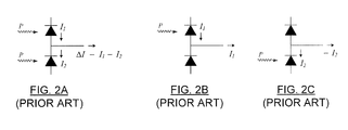
- FIG. 2A , 2 B and 2 C depicts the three illumination conditions required to measure the CMRR.
- a weak photocurrent ⁇ I is measured while strong photocurrents I 1 and ⁇ I 2 are detected under single-photodiode illumination ( FIGS. 2B and 2C ).
- the CMRR is defined here as the ratio of these values:
- CMRR ⁇ ⁇ ⁇ ⁇ I ⁇ ⁇ I 1 ⁇ + ⁇ I 2 ⁇ ( 1 )
- CMRR complementary metal-oxide-semiconductor
- CMRR complementary metal-oxide-semiconductor
- the balanced detection device is understood to include a pair of input waveguides, a pair of output waveguides respectively connected to a pair of photodiodes coupled to generate a differential output current, and an optical mixing element coupling light between the input waveguides and the output waveguides.
- the method includes the following steps of:
- the method above is particularly appropriate for characterizing coherent receivers where the optical mixing element is embodied by an optical hybrid mixer.
- an apparatus for measuring a factor characterizing a balanced detection device including a pair of input waveguides, a pair of output waveguides respectively connected to a pair of photodiodes coupled to generate a differential output current, and an optical mixing element coupling light between the input waveguides and the output waveguides.
- the apparatus includes an optical assembly having a light source assembly for generating a modulated seed light signal, a splitter for splitting the modulated seed light signal into two light components thereof, first and second signal branches having inputs connected to the splitter for respectively receiving the components of the modulated seed light signal therefrom and outputs operatively connectable the pair of input waveguides of the balanced detection device.
- the optical assembly further includes a phase modulator provided in one of the first and second branches for varying a phase of the light component therein.
- the apparatus further includes a controller connectable to the balanced detection device to receive therefrom the differential output current.
- the controller controls the optical assembly to perform the following steps:
- FIG. 1 is a schematic representation of a typical optical front-end (OFE) such as found in a coherent receiver.
- OFE optical front-end
- FIGS. 2A , 2 B and 2 C schematically illustrates the illumination conditions for determining the CMRR of a pair of balanced photodiodes, respectively under dual-photodiode illumination ( FIG. 2A ) and single-photodiode illumination ( FIGS. 2B and 2C ).
- FIG. 3 schematically illustrates a balanced detection device of simple configuration.
- FIG. 4 illustrates a step of injecting a single-port test signal in the balanced detection device of FIG. 3 .
- FIG. 5 illustrates a step of injecting dual-port test signals in the balanced detection device of FIG. 3 .
- FIG. 6 schematically illustrates another embodiment of a balanced detection device where signals are mixed by a 90° optical hybrid mixer.
- FIG. 7 is a graph showing SPRR as a function of the frequency for different imbalance and skew, according to simulations.
- FIG. 8A illustrates an apparatus for measuring the SPRR of an optical front end and the use of this apparatus within a step of injecting dual-port test signals in the optical front end;
- FIG. 8B illustrates the use of the same apparatus within a step of injecting a single-port test signal in the optical front end.
- FIG. 9 is a graph showing the RF power of the differential output current as a function of the modulation frequency using the configuration in FIG. 8A for two successive scans and maximum curve over 18 successive scans.
- FIGS. 10A and 10B are graphs showing the RF power of the differential output current as a function of the modulation frequency using the configuration in FIG. 8A for a single scan ( FIG. 10A ) and maximum curve over 18 successive scans ( FIG. 10B ), and a comparison with the RF power measured when only one photodetector is connected ( FIG. 10B ).
- FIG. 11 is a graph showing the RF power of the differential output current as a function of the modulation frequency using the configuration in FIG. 8B .
- FIG. 12 is a graph comparing the measured SPRR, the theoretical SPRR and the measured CMRR as a function of the frequency.
- the present invention generally relates to a method an apparatus for characterizing a balanced detection device.
- balanced detection device is understood to refer to any assembly of components where a pair of input signals are combined to produce a pair of output signals carrying the same individual intensities but beats that are out of phase, the output signals being detected differentially by balanced photodiodes. Individual intensities are thus subtracted, whereas the beat intensities are added, doubling the amplitude of the meaningful photocurrent. Balanced detection thus allows using all of the received signal power for detection, while rejecting common-mode signals.
- the balanced detection device 20 includes a pair of input waveguides 22 a and 22 b , a pair of output waveguides 24 a and 24 b respectively connected to a pair of photodiodes 26 a and 26 b coupled to generate a differential output current 28 .
- An optical mixing element 30 couples light between the input waveguides 22 a and 22 b and the output waveguides 24 a and 24 b .
- the light outputted by each output waveguide 24 a and 24 b is a mix of the signal injected in both input waveguides 22 a and 22 b .
- the optical mixing element 30 is a 3 dB coupler in which an optical signal of interest E s (t) is mixed with a local oscillator field E LO (t).
- balanced detection devices such as those used for coherent detection can differ from the simple embodiment shown in FIG. 3 .
- the illustrated balanced detection device includes a plurality of pairs of input waveguides 22 a and 22 b , output waveguides 24 a and 24 b and photodiodes 26 a and 26 b , mixed in various fashions by two optical mixing elements 30 here embodied by 90° optical hybrid mixers.
- the method of the present invention may be applied to any and all combinations of pairs of input waveguides 22 a and 22 b and output waveguides 24 a and 24 b of such a balanced detection device 30 coupled together by one of the optical mixing elements 30 .
- waveguide is understood herein to refer any appropriate light-guiding structures such as optical fibers or planar or channel waveguides.
- the photodiodes may be embodied by any device apt to convert light into an electrical current.
- the optical mixing element may be embodied by any device or assembly of devices combining input light signals to provide mixed output light signals, such as optical couplers and hybrid mixers.
- the output photocurrents measured by the photodiodes 26 a and 26 b are respectively given by:
- Each photocurrent comprises three contributions.
- the first two are proportional to the individual power of each interfering field, while the third one is proportional to an interference term dependent on the relative phase between the fields.
- this interference term oscillates at the beat frequency ⁇ s - ⁇ LO .
- Ideal balanced detection thus doubles the photocurrent associated to the interference beats while rejecting those associated to the individual optical field powers.
- photocurrents I 1 and I 2 of individual photodiodes 26 a and 26 b cannot be measured without blocking the light in one output waveguide 24 a and 24 b of the device 20 .
- This is not possible, in general, when characterizing a coherent receiver OFE in which the photodiodes 26 a and 26 b and the optical mixing element 30 are integrated and individually inaccessible. It is more convenient to compare the weak signal measured under the configuration shown in FIG. 4 to the strong signal measured under the configuration shown in FIG. 5 . In this new configuration, two optical fields having the same amplitude are launched into the coupler. Depending on their relative phase, a strong output signal can be generated.
- the relative phase ⁇ can be adjusted such that all the light reaches a single photodiode, thus replicating the conditions of the single-photodiode illumination of FIG. 2 .
- the optical field amplitude in FIG. 5 is half that in FIG. 4 in order to illuminate the photodiodes with the same optical power.
- the differential output current ⁇ I dual is somewhere between two extreme values of strong amplitude: ⁇
- a single-port rejection ratio is defined as the ratio of the weak photocurrent under single-port, ⁇ I 0 , illumination to the strong measurable photocurrents ⁇ I 1 and ⁇ I 2 under dual-port illumination:
- the SPRR is representative not only of unequal responsivities of the photodiodes, but also of an uneven split of the input power by the coupler. Furthermore, the SPRR measured with one input port is not necessarily equal to that measured with the other input port. For example, it may happen that unequal photodiode responsivities compensate for an uneven split by the coupler such that the differential current ⁇ I 0 measured from one input port vanishes. Both defects will however add-up when measuring ⁇ I 0 from the other input port. Finally, the SPRR is better adapted to coherent detection in that, referring to Eqs.
- a method for measuring a factor characterizing a balanced detection device i.e. the SPRR explained above.
- a simple embodiment of this method is best understood with reference to FIGS. 4 and 5 , where a balanced detection device 20 of a same construction as the device 20 of FIG. 3 , is shown, and therefore includes a pair of input waveguides 22 a and 22 b , a pair of output waveguides 24 a and 24 b respectively connected to a pair of photodiodes 26 a and 26 b coupled to generate a differential output current 28 , and an optical mixing element 30 coupling light between the input waveguides 22 a and 22 b and the output waveguides 24 a and 24 b.
- the method includes a step of injecting a pair of modulated dual-port test signals 32 a and 32 b in the pair of input waveguides 22 a and 22 b , respectively.
- This injecting can be performed by any appropriate optical assembly, i.e. any device or combination of devices which is apt to generate light, modify its optical properties as may be required, and input such light within the balanced detection device for propagation into the input waveguides 22 a and 22 b .
- the dual-port test signals 32 a and 32 b have equivalent optical field amplitudes E/2 and a relative phase ⁇ therebetween.
- the differential output current 28 of the photodiodes 26 a and 26 b is then measured, by any appropriate current detector as well known in the art, for values of the relative phase ⁇ corresponding to light primarily reaching each one of the photodiodes 26 a and 26 b .
- the maximized differential output currents ⁇ I 1 and ⁇ I 2 can be obtained as corresponding to the largest positive and negative values respectively.
- the method also includes injecting, via the optical assembly, a modulated single-port test signal 34 in a single one of the input waveguides, shown as input waveguide 22 a in the illustrated example.
- the single-port test signal 34 has an optical field amplitude E corresponding to twice the optical field amplitude E/2 of the dual-port test signals 32 a and 32 b .
- E optical field amplitude
- the single-port test signal 34 corresponds to an optical power for the single-port test signal 34 which is four times the optical power of each dual-port test signal 32 a or 32 b , since, by definition, the optical power corresponds to the square of the optical field amplitude. This ensures illuminating the photodiodes with the same optical powers as in FIG. 2 in the particular case where the optical phase ⁇ in the setup of FIG. 5 is adjusted such as transmitting all the optical power to only one of the photodiode.
- the corresponding differential output current 28 is measured, thereby obtaining a single-port differential output current ⁇ I 0 .
- the single-port rejection ratio SPRR can then be calculated according to equation (8) above, i.e. calculating the ratio of the single-port differential output current ⁇ I 0 to the sum of the maximized differential output currents ⁇ I 1 and ⁇ I 2 .
- the single-port rejection ratio is representative of the ratio of the weak photocurrent under illumination of a single-port, i.e. a single input waveguide, to the strong measurable photocurrents under illumination of both input waveguides. It will therefore be understood that the value obtained for the SPRR is directly associated to the input waveguide in which the single-port test signal is injected.
- the method preferably includes performing, sequentially, the step of injecting a single-port test signal 34 in each of the input waveguide 22 a and 22 b , and performing the calculating of the SPRR using each of the measured single-port differential output current 28 . A value for the SPRR associated with each input waveguide 22 a and 22 b is therefore obtained.
- the SPRR is explained above with reference to the simple design of the balanced detection device of FIGS. 3 to 5 , it also applies to more complex designs, such as the complete optical front-end (OFE) shown in FIG. 1 , which includes a plurality of pairs of input waveguides 22 a and 22 b , output waveguides 24 a and 24 b and photodiodes 26 a and 26 b , connected to two optical hybrid mixers respectively associated with x and y polarization stages.
- OFFE optical front-end
- each of these SPRR values can be obtained using the steps of the method defined above.
- the notion of “port” differs from the notion of “input waveguide”, as the signal from each input port S and LO is divided into two input waveguides (input waveguides 22 a for port S and input waveguides 22 b for port LO) respectively connected to one of the two optical mixing elements 30 of the device.
- One skilled in the art will know to adapt the power of the dual-port test signals and single-port test signal to take this factor into consideration and ensure the proper ratio of the power of the signals actually injected in the input waveguides.
- the mixing and splitting of the input optical signals is performed by the 90° optical hybrid mixers, embodying mixing elements 30 of the balanced detection device 20 more complex than the one of FIG. 3 .
- This part of the OFE is replicated in FIG. 6 , where E 1 (t) to E 4 (t) represent the optical fields at the photodiodes 26 a and 26 b of a given pair for the input conditions shown.
- the input waveguides 22 a and 22 b respectively receive optical signals from input ports S and LO of the OFE, embodying the dual-port test signals 32 a and 32 b of the method described above.
- the phase ⁇ can be chosen to maximize or minimize the differential output current 28 .
- ⁇ I 1 ( t ) R ⁇
- ⁇ I 2 ( t ) R ⁇
- Equations (18) and (19) provide expressions for the two strong photocurrents discussed above, thus allowing calculation of the denominator of the SPRR as defined in Eq. (8).
- this can be represented by Eq. (14) in which field E s is doubled and coefficients a Li are put to 0.
- the SPRR can be calculated according to definition (8).
- FIGS. 8A and 8B An apparatus 36 which can be used to implement this method is also shown.
- the apparatus 36 preferably includes an optical assembly 37 , in which is provided a light source assembly 38 for generating a modulated seed light signal 43 .
- the light source assembly 38 is here shown as including a laser source 39 , such as for example a semiconductor laser generating a seed light signal 40 and followed by an amplitude modulator 41 which imposes a modulation to the seed light signal 40 , thereby obtaining the modulated seed light signal 43 .
- the modulation may be sinusoidal, although other periodic forms or a pulsing modulation could be used without departing from the scope of the invention.
- the optical assembly further includes a splitter 42 , such as a 50/50 beamsplitter for splitting the modulated seed light signal 43 into two light components 44 a and 44 b .
- First and second signal branches 46 a and 46 b having inputs 48 a and 48 b are connected to the splitter 42 for respectively receiving the components 44 a and 44 b of the modulated seed light signal 43 therefrom and have outputs 50 a and 50 b operatively connectable to the pair of input waveguides 22 a and 22 b of the balanced detection device 30 .
- the outputs 50 a and 50 b can only be connected to the ports S and LO of the OFE, whose internal components lead portions of the light received at each port to one of the optical hybrid mixers 30 .
- a phase modulator 52 is provided in one of the first and second branches 46 a or 46 b for varying the phase of the light component 44 a or 44 b circulating in this branch.
- the phase modulator may be embodied by a material providing a linear electro-optic effect.
- the phase modulator 52 is shown in the second branch 46 b in the illustrated embodiment, connected to the port LO of the OFE, one skilled in the art will readily understand that the phase modulator 52 could alternatively be provided in the first branch 46 a , or that in another alternative two phase modulators may be provided, one in each branch.
- the optical assembly 37 may also include, in one or both branches 46 a and 46 b , a variable optical attenuator 56 and a variable delay line 58 .
- a polarisation controller 54 is further preferably provided in the first branch 46 a , connected to port S of the OFE. The function of these components will become apparent from the description below of the operation of the apparatus 36 .
- the apparatus 36 finally includes a controller 60 .
- the controller has an input connectable to the balanced detection device 20 to receive therefrom the differential output current 28 , and various outputs connected to the various components of the optical assembly 37 .
- the controller sends appropriate signals to the optical assembly 37 to control the same to perform the steps of the method according to the invention.
- the controller 60 may be embodied by a variety of devices or systems including multiple devices as well known in the art.
- the controller may also have a user input 62 for receiving instructions from a user, for example through knobs, keys, a keyboard or any other appropriate interface.
- the user input 62 may alternatively or additionally be connected to other devices providing the controller 60 with control parameters for one or more of the devices of the optical assembly 37 .
- FIG. 8A illustrates the setup used to inject the dual-port test signals 32 a and 32 b into the respective input waveguides 22 a and 22 b of one of the optical hybrid mixers of the OFE embodying the optical mixing element 30 .
- the laser source 39 generates the seed signal 40 which is then modulated by the amplitude modulator 41 , according to a sinusoidal modulation.
- the resulting modulated seed signal 43 is then separated by the splitter 42 so that two equivalent components of the modulated seed light signal 43 propagate in the first and second branches 46 a and 46 b .
- “equivalent” light components it is understood that they are coherent and both have the same optical characteristics.
- the initial power in the modulated seed light signal 43 is split evenly between the two light components, although this is not necessary in the illustrated embodiment, as will become apparent from the description below.
- the first to branch 46 a is connected to the port S of the OFE while the second branch 46 b is connected to the port LO.
- the LO port is destined, in usual operation, to receive a reference signal LO of is a known polarization state.
- the LO signal is evenly split into two equal LO signals of orthogonal polarization, each sent as input to one of the x and y polarization stages associated with the optical hybrid mixers.
- the power launched at port LO is equally split among the two polarization stages.
- the power of the signal reaching the optical mixing element 30 of the x polarization stage through the input waveguide 22 b will be a fourth of the initial power of the modulated seed light signal 43 , also assuming an even split of the modulated seed light signal 43 between the two branches 46 a and 46 b.
- the port S is destined, in usual operation, to receive a signal S of unknown polarization.
- the S signal is split into its two orthogonal x and y polarization components, each sent as input to one of the polarization stages associated with the optical hybrid mixers.
- the power inputted at the port S is randomly distributed between the two polarization stages, this factor having no significant impact of the measure to be made.
- the VOA 56 a in the first branch 46 a can be used to attenuate the signal therein until the measured output of the first branch 46 a correspond to half the output of the second branch 46 b .
- another VOA can also be provided in the second branch 46 b to perform other adjustments, in which case the overall power in both branches would be diminished accordingly.
- the outputs 50 a and 50 b of both branches 46 a and 46 b can be temporarily connected to appropriate light detectors (not shown) for this purpose.
- the method preferably includes using the polarization controller 54 in the first branch 46 a .
- the polarization controller 54 is preferably controlled to adjust the polarisation state of the light in the first branch 46 a such that all the light signal is transmitted to the polarisation stage under investigation (the x polarisation stage in the case of the illustration shown in FIG. 8A ).
- the corresponding variation of the differential output current 28 is measured during this process.
- the differential current varies between two maxima as the phase of the light is varied by the phase modulator 52 .
- the amplitude of these maxima also varies from a highest value, corresponding to all the light from port S going to the x polarisation stage, to a lowest value (i.e. null) corresponding to all the light from port S going to the y polarisation stage.
- the polarisation state of the light in the first branch 46 a can therefore be fixed by the polarisation controller 54 to a state for which the differential output current is maximum.
- the technique described above provides, in the input waveguide 22 a and 22 b , the dual-port test signals 32 a and 32 b of equal power required by the method according to embodiments if the invention.
- the relative phase of these test signals must also be adjusted, sequentially, in order to ensure that light primarily reaches each one of the photodiodes 26 a and 26 b , in order to measure the corresponding maximized differential output currents ⁇ I 1 and ⁇ I 2 .
- This may for example be accomplished by using the phase modulator 52 .
- the optical phase of the light component in the second branch 46 b is gradually shifted over time with the phase modulator 52 to vary the relative phase ⁇ so as to produce a differential output current 28 with varying amplitude.
- the shifting of the relative phase should be performed significantly slower than the amplitude modulation provided by the intensity modulator 41 .
- the variation of the differential output current 28 is measured as a function of the relative phase ⁇ . From equation (6) above, wherein the relative phase corresponds to the difference between the individual phase terms ⁇ s (t) ⁇ LO (t), it can be seen that the differential output current 28 will theoretically oscillate between two maxima, corresponding to the cases where all the light goes to each photodiode 26 a or 26 b , respectively. These two maxima therefore provide the value of the dual-port differential output currents ⁇ I 1 and ⁇ I 2 , respectively.
- the method may involve simply identifying a single maximum in the variation of the differential output current 28 , and setting both maximized differential output currents ⁇ I 1 and ⁇ I 2 to this value.
- the method may involve delaying the light component in one or both of the branches 46 a and 46 b , using a variable delay line 58 a or 58 b in the corresponding branch 46 a or 46 b .
- the dual-port test signals 32 a and 32 b are modulated, it may be preferable to ensure that they are fully synchronized at the input of the optical mixing element 30 .
- This synchronization is optimized when the differential delay between both light paths between the splitter 42 and the mixing element 30 is minimized. It can be adjusted by ensuring that the differential output current 28 of maximum amplitude over the phase modulator cycle is the largest possible.
- variable delay lines 58 a and 58 b can therefore be used to vary the relative delay between the dual-port test signals 32 a and 32 b .
- a measure of the variation of the differential output current 28 as a function of the delay imposed by the variable delay lines 58 a and 58 b can provide the delay for which this differential output current 28 is maximum, corresponding to the best achievable synchronization between the two is dual-port test signals.
- 32 a and 32 b For better adjustment, this synchronisation is better performed at a high frequency of the modulation provided by the intensity modulator 41 .
- the measure of the single-port differential output current ⁇ I 0 is simpler than the measure of the maximized differential output currents ⁇ I 1 and ⁇ I 2 , since synchronization is not an issue with a single test signal.
- FIG. 8B there is shown an example of a setup using the same apparatus 36 as the one of FIG. 8A , where the first branch 46 a is used to inject the single-port test signal into the port S, and therefore the first waveguide 22 a .
- the polarization controller 54 is kept adjusted in the same manner as for the previous step such that one can still assume that most of the power launched into port S is directed to the polarization stage under test.
- the VOA in the first branch 46 a must be adjusted such that the power launched into the OFE is increased by a factor of 4 with respect to the previous step, in order for the single-port test signal 34 to have four times the power of the individual dual-port test signals.
- the differential output current 28 can then be used directly as the single-port differential output current ⁇ I 0 , and the SPRR calculated using equation (8) above.
- the SPRR for the second waveguide 22 b of the same hybrid mixer 30 can be obtained by following the same procedure with the output one of the first branch and second branches 46 a or 46 b connected to the port LO, adjusting the optical power and phase accordingly.
- the same procedure can be followed using the differential output signal 28 ′ for the other set of photodiodes of the x polarization stage, as well as for both sets of photodiodes of the y polarization stage, yielding the 8 SPRR values associated with the OFE.
- the SPRR provides valuable information on the performance of the is tested balanced detection device.
- the value of the SPRR should be zero, as the differential output current of the device should be zero if the light from the characterized input waveguide is perfectly split between the two output waveguides and if both photodiodes have exactly the same responsitivity.
- the CMRR of balanced photodiodes is usually specified as a function of frequency, since their frequency responses may differ.
- the SPRR calculated from expressions (18)-(20) can still present a frequency dependence. This is so because of a possible skew between the propagation times from an input port to each photodiode of a pair of balanced detectors. Rejection of a modulated input power can be degraded, especially if this skew becomes comparable to the characteristic period of the modulation.
- the SPRR definition in Eq. (8) is transformed into:
- Eq. (21) only the amplitude of the complex expressions resulting from the Fourier transforms are taken, which corresponds to considering only the amplitude of the photocurrents and not their phases.
- the notation in Eq. (22) is also a reminder that such SPRR parameter is required to characterize the rejection of each input power by each pair of balanced detectors.
- Four parameters are thus required in the case of the hybrid shown in FIG. 6 , whereas eight parameters are needed in the case of an OFE with polarization diversity.
- the delay ⁇ represents the skew between the two output paths and should ideally be zero.
- the SPRR is shown on a log scale as a function of frequency, as calculated with Eq. (22) for different combinations of skew ⁇ and imbalance ⁇ sI .
- the SPRR is found to depend very weakly on ⁇ LI and ⁇ I , which have been set to 0 and 1 respectively in the calculations shown in FIG. 7 .
- the skew is responsible for the frequency dependence of the SPRR.
- the 90° optical hybrid mixer has a strong impact on the level of rejection achieved with the balanced detection.
- the following describes a particular experimental setup constructed to test the method proposed for the measurement of the SPRR.
- the following can also be viewed as a preferred embodiment of an apparatus implementing the method described above.
- a Lightwave Components Analyzer (LCA) model 8703A from Agilent fed with a DFB laser provided the intensity modulated optical signal at a frequency scanned from 130 MHz to 20 GHz together with the detection system.
- LCA Lightwave Components Analyzer
- the configuration in FIG. 8 a was built using a 3 dB fiber coupler, two VOAs, and a lithium niobate phase modulator. Fiber patch cords of adjusted lengths were used as delay lines.
- the FSR of the interferometer formed by the measurement setup was measured to be 250 GHz, thus corresponding to a differential delay of 4 ps between the two arms.
- the optical powers were adjusted to 17 ⁇ W in both the S and LO ports.
- the phase modulator was fed with a triangular wave at a frequency of 1 Hz and an amplitude slightly larger than required to produce a phase modulation of ⁇ .
- a polarization controller on arm S was adjusted to maximize the interference signal.
- FIG. 9 shows the RF power of the measured output modulated signal as a function of the frequency during two successive scans, as well as the curve of maximum values over 18 successive scans.
- FIG. 9 shows the frequency response over a limited range of 5 GHz to better show the difference from scan to scan.
- FIGS. 10A and 10B the whole frequency response is shown from 0 to 20 GHz for a single scan as well as for the maximum over 18 scans.
- the phase of the measured modulation could serve at distinguishing between the strong photocurrents ⁇ I 1 and ⁇ I 2 , only the maximum between these two was selected and used as the denominator of the SPRR.
- Arm LO of the interferometer was disconnected as per FIG. 8 b .
- the VOA in arm S was adjusted to 68 ⁇ W in port S, thus a factor 4 larger than the power used in the dual-port measurement.
- the resulting output signal RF power as a function of the modulation frequency is shown in FIG. 11 and was used as the numerator of the SPRR.
- FIG. 12 Shown in FIG. 12 is the SPRR taken as the ratio of the curve in FIG. 11 and twice the maximum curve in FIG. 10B , together with a fit to Eq. (22).
- photocurrents I 1 and I 2 on individual photodiodes were also measured using a successive disconnection of the fiber-connected photodiodes in the setup in FIG. 8 b .
- the RF powers measured under this single-port illumination (and single-photodiode as well) are also shown in FIG. 10B .
- the sum of these two photocurrents was used as the denominator of the CMRR, which is also shown in FIG. 12 .
- the SPRR a parameter that can be measured end-to-end on the OFE provides virtually the same information as the well known CMRR which requires disconnection inside the OFE to access the photocurrents of individual photodiodes.
- the CMRR and SPRR shown in FIG. 12 contains the same noise, which is mainly determined by their common numerator, i.e. the signal shown in FIG. 11 .
- the good match with the theoretical expression is an indication that in this case, the performance of the balanced detection was mainly determined by the characteristics of the 90° optical hybrid mixer.
- methods and instruments according to embodiments of the invention can be used to qualify coherent receivers making use of balanced detection or more generally any type of optical receivers making use of balanced detection.
- Such qualification can assess whether the receiver meets the specifications for the SPRR (pass/fail test) or any other parameter that can be deduced from the SPRR (imbalance, skew, frequency response, etc.).
- the measurement the SPRR gives information on the imbalance (difference in electrical current generated in each photodiode due to optical loss, responsitivity, polarization dependent loss, etc.) and skew (difference in optical path length from the input to each photodetector). The measurement can thus serve to trim either of these two parameters or both and improve the performance of the balanced receiver.
- the receiver can afterwards be qualified as described in the previous point.
Abstract
Description
- a) injecting a pair of modulated dual-port test signals in the pair of input waveguides, respectively. The dual-port test signals have a same optical power and have a relative phase φ therebetween;
- b) measuring the differential output current of the photodiodes for values of the relative phase φ corresponding to light primarily reaching each one of the photodiodes. In this manner, maximized differential output currents ΔI1 and ΔI2 are obtained;
- c) injecting a modulated single-port test signal in a single one of the input waveguides. The single-port test signal has an optical power corresponding to four times the optical power of each of the dual-port test signals. The corresponding differential output current is then measured, and a single-port differential output current ΔI0 is obtained; and
- d) calculating a single-port rejection ratio SPRR corresponding to the ratio of the single-port differential output current ΔI0 to the sum of the maximized differential output currents ΔI1 and ΔI2.
- a) injecting, via an optical assembly, a pair of modulated dual-ports test signals in the pair of input waveguides, respectively, the dual-ports test signals having a same optical power and a relative phase φ therebetween;
- b) measuring the differential output current of the photodiodes for values of the relative phase φ corresponding to light primarily reaching each one of the photodiodes, thereby obtaining maximized differential output currents ΔI1 and ΔI2;
- c) injecting, via said optical assembly, a modulated single-port test signal in a single one of the input waveguides, the single-port test signal having an optical power corresponding to four times the optical power of each of the dual-port test signals, and measuring the corresponding differential output current, thereby obtaining a single-port differential output current ΔI0; and
- d) calculating a single-port rejection ratio SPRR corresponding to the ratio of the single-port differential output current ΔI0 to the sum of the maximized differential output currents ΔI1 and ΔI2.
E s(t)=√{square root over (P s(t))}·exp(jφ s(t))·exp(jω s t), (2)
E LO(t)=√{square root over (P LO(t))}·exp(jφ LO(t))·exp(jω LO t) (3)
ΔI(t)=I 1(t)−I 2(t)=2R√{square root over (P s(t)P LO(t))}{square root over (P s(t)P LO(t))}·sin((ωs−ωLO)·t+φ s(t)−φLO(t)). (6)
−|ΔI2|≦ΔIdual≦|ΔI1|, (7)
where ΔI1 or ΔI2 is the differential output current measured when φ is such that the power incident on the corresponding photodiode is maximized.
E 1(t)=a s1 E s(t−τ s1)+a L1 e jφ E s(t−τ−τ L1), (9)
E 2(t)=a s2 E s(t−τ s2)+a L2 e jφ E s(t−τ−τ L2), (10)
E 3(t)=a s3 E s(t−τ s3)+a L3 e jφ E s(t−τ−τ L3), (11)
E 4(t)=a s4 E s(t−τ s4)+a L4 e jφ E s(t−τ−τ L4), (12)
where asi and aLi are coupling coefficients between input ports S or LO and the four output ports, whereas τsi and τLi are the time delays from input port S or LO to the four outputs. It is to be noted that is such a configuration, the optical hybrid mixer couples light from two
τ+τLi=τsi, (13)
for all paths simultaneously.
ΔI(t)=R|E s(t−τ s1)|2·(|a s1|2 +|a L1|22|a s1 ∥a L1|cos θ)−R|E s(t−τ s2)|2·(|a s2|2 +|a L2|22|a s2 ∥a L2|cos θ) (14)
where
θ=φ+arg(a L1)−arg(a s1)=φ+arg(a L2)−arg(a s2). (15)
ΔI 1(t)=R{|E s(t−τ s1)|2·(|a s1 |+|a L1|)2 −|E s(t−τ s2)|2·(|a s2 |−|a L2|)2}, (16)
ΔI 2(t)=R{|E s(t−τ s1)|2·(|a s1 |+|a L1|)2 −|E s(t−τ s2)|2·(|a s2 |−|a L2|)2}. (17)
ΔI 1(t)≈R·|E s(t−τ s1)|2·(|a s1 |+|a L1|)2, (18)
ΔI 2(t)≈R·|E s(t−τ s2)|2·(|a s2 |+|a L2|)2. (19)
ΔI 0(t)=4R·{|a s1|2 ·|E s(t−τ s1)|2 −|a s2|2 ·|E s(t−τ s2)|2}. (20)
where it now characterizes the rejection of a sinusoidal power modulation at frequency f. Using the amplitude of the Fourier transform of Eqs. (18) to (20) as the frequency-dependent photocurrents, one obtains:
Claims (17)
Priority Applications (1)
| Application Number | Priority Date | Filing Date | Title |
|---|---|---|---|
| US12/916,137 US8406621B2 (en) | 2009-10-29 | 2010-10-29 | Method and apparatus for measuring a factor characterizing a balanced detection device |
Applications Claiming Priority (2)
| Application Number | Priority Date | Filing Date | Title |
|---|---|---|---|
| US25602609P | 2009-10-29 | 2009-10-29 | |
| US12/916,137 US8406621B2 (en) | 2009-10-29 | 2010-10-29 | Method and apparatus for measuring a factor characterizing a balanced detection device |
Publications (2)
| Publication Number | Publication Date |
|---|---|
| US20110129213A1 US20110129213A1 (en) | 2011-06-02 |
| US8406621B2 true US8406621B2 (en) | 2013-03-26 |
Family
ID=44068993
Family Applications (1)
| Application Number | Title | Priority Date | Filing Date |
|---|---|---|---|
| US12/916,137 Active 2031-09-27 US8406621B2 (en) | 2009-10-29 | 2010-10-29 | Method and apparatus for measuring a factor characterizing a balanced detection device |
Country Status (1)
| Country | Link |
|---|---|
| US (1) | US8406621B2 (en) |
Cited By (15)
| Publication number | Priority date | Publication date | Assignee | Title |
|---|---|---|---|---|
| US20120020669A1 (en) * | 2010-07-20 | 2012-01-26 | U2T Photonics Ag | Method and system for characterizing an optical device |
| US20140205280A1 (en) * | 2013-01-22 | 2014-07-24 | Electronics And Telecommunications Research Institute | Measuring device and method of measuring signal transmission time difference thereof |
| US9106334B2 (en) | 2013-05-16 | 2015-08-11 | Exfo Inc. | Method and system for common-mode-rejection-ratio (CMRR) characterization of an integrated coherent receiver |
| US9806806B1 (en) | 2016-07-07 | 2017-10-31 | Elenion Technologies, Llc | Coherent optical receiver testing |
| US9806822B1 (en) | 2016-07-07 | 2017-10-31 | Elenion Technologies, Llc | Coherent optical receiver testing |
| US9941973B2 (en) | 2016-08-29 | 2018-04-10 | Ciena Corporation | Phase modulator with reduced residual amplitude modulation |
| US10014955B1 (en) * | 2015-04-24 | 2018-07-03 | Vencore Labs, Inc. | Signal processing circuit with optical local oscillator signal |
| CN109450529A (en) * | 2018-12-06 | 2019-03-08 | 南京牧镭激光科技有限公司 | Detection device and detection method |
| US20190379462A1 (en) * | 2018-06-08 | 2019-12-12 | Maxim Integrated Products, Inc. | Systems and methods for polarization control using blind source separation |
| US11022825B2 (en) | 2018-09-03 | 2021-06-01 | Ciena Corporation | Silicon photonics modulator using TM mode and with a modified rib geometry |
| US11226504B2 (en) | 2019-07-19 | 2022-01-18 | Ciena Corporation | Free-carrier absorption variable optical attenuators and thermal phase shifters formed by an optical waveguide having multiple passes in an intrinsic region |
| US20220158726A1 (en) * | 2013-03-15 | 2022-05-19 | Nec Corporation | Optical transmission/reception device, optical communications system and optical transmission/reception method |
| US11683092B2 (en) | 2020-02-24 | 2023-06-20 | Ciena Corporation | Loss-based wavelength meter |
| US20230194906A1 (en) * | 2017-12-29 | 2023-06-22 | Lumentum Technology Uk Limited | Balancing losses in semiconductor optical waveguides |
| US11768391B2 (en) | 2021-02-05 | 2023-09-26 | Ciena Corporation | Carrier depletion-based silicon photonic modulator using capacitive coupling |
Families Citing this family (11)
| Publication number | Priority date | Publication date | Assignee | Title |
|---|---|---|---|---|
| KR20130068156A (en) | 2011-12-14 | 2013-06-26 | 한국전자통신연구원 | Apparatus for measurement of coherent optical receiver |
| CN103840889B (en) * | 2014-03-24 | 2016-06-08 | 武汉光迅科技股份有限公司 | A kind of tests polarization multiplexing balanced coherent receives the device and method of machine common mode rejection ratio |
| GB2524566B (en) * | 2014-03-27 | 2020-05-06 | Oxley Dev Company Ltd | Light assembly with integrated test facility |
| US9768864B2 (en) * | 2014-11-21 | 2017-09-19 | Tektronix, Inc. | Test and measurement device for measuring integrated coherent optical receiver |
| US9841447B2 (en) * | 2014-11-21 | 2017-12-12 | Tektronix, Inc. | Apparatus enabling use of a reference diode to compare against a device under test in relative amplitude and phase measurements |
| CN106160847B (en) * | 2016-06-29 | 2018-12-25 | 武汉光迅科技股份有限公司 | A kind of tests polarization is multiplexed the device and method of integrated coherent receiver photoelectricity bandwidth |
| CN106411399B (en) * | 2016-08-31 | 2019-02-19 | 武汉光迅科技股份有限公司 | The automatic test approach and device of two-in-parallel MZI type electrooptic modulator optical loss |
| US10651947B2 (en) * | 2018-02-20 | 2020-05-12 | Futurewei Technologies, Inc. | Coherent detection with remotely delivered local oscillators |
| CN109194411B (en) * | 2018-09-27 | 2020-12-01 | 武汉光迅科技股份有限公司 | Device and method for measuring photoelectric responsivity of silicon optical coherent receiver |
| US11209459B2 (en) | 2019-02-15 | 2021-12-28 | Texas Instruments Incorporated | Common mode rejection ratio test system and method |
| US20230299855A1 (en) * | 2022-03-17 | 2023-09-21 | Ciena Corporation | Coherent receiver having low VOA-induced phase changes |
Citations (4)
| Publication number | Priority date | Publication date | Assignee | Title |
|---|---|---|---|---|
| US5463461A (en) * | 1991-03-06 | 1995-10-31 | Kokusai Denshin Denwa Company, Ltd. | Coherent optical receiver having optically amplified local oscillator signal |
| US6859586B2 (en) | 2002-06-28 | 2005-02-22 | Nortel Networks Limited | 3 Fibre I and Q coupler |
| US20050135489A1 (en) * | 2003-12-17 | 2005-06-23 | Andrew Ho | Noise-tolerant signaling schemes supporting simplified timing and data recovery |
| US20110228280A1 (en) * | 2010-03-17 | 2011-09-22 | Lightlab Imaging, Inc. | Intensity Noise Reduction Methods and Apparatus for Interferometric Sensing and Imaging Systems |
-
2010
- 2010-10-29 US US12/916,137 patent/US8406621B2/en active Active
Patent Citations (5)
| Publication number | Priority date | Publication date | Assignee | Title |
|---|---|---|---|---|
| US5463461A (en) * | 1991-03-06 | 1995-10-31 | Kokusai Denshin Denwa Company, Ltd. | Coherent optical receiver having optically amplified local oscillator signal |
| US6859586B2 (en) | 2002-06-28 | 2005-02-22 | Nortel Networks Limited | 3 Fibre I and Q coupler |
| US20050135489A1 (en) * | 2003-12-17 | 2005-06-23 | Andrew Ho | Noise-tolerant signaling schemes supporting simplified timing and data recovery |
| US20070297520A1 (en) * | 2003-12-17 | 2007-12-27 | Rambus Inc. | Noise-tolerant signaling schemes supporting simplified timing and data recovery |
| US20110228280A1 (en) * | 2010-03-17 | 2011-09-22 | Lightlab Imaging, Inc. | Intensity Noise Reduction Methods and Apparatus for Interferometric Sensing and Imaging Systems |
Non-Patent Citations (13)
| Title |
|---|
| 107-Gb/s full-ETDM transmission over field installed fiber using vestigial sideband modulation S. L. Jansen, R. H. Derksen, C. Schubert, X. Zhou, M. Birk, C.-J. Weiske, M. Bohn, D. van den Borne, P. M. Krummrich, M. Möller, F. Horst, B. J. Offrein, H. de Waardt, G. D. Khoe and A. Kirstädter Optical Society of America, 2006, 3 pages. |
| Bach: "Ultra-broadband photodiodes and balanced detectors towards 100 Gbit/s and beyond", Proc. of SPIE, vol. 6014 60140B, 2005, pp. 1-13. * |
| Coherent Equalization and POLMUX-RZ-DQPSK for Robust 100-GE Transmission Chris R. S. Fludger, Thomas Duthel, Dirk van den Borne, Christoph Schulien, Ernst-Dieter Schmidt, Torsten Wuth, Jonas Geyer, Erik De Man, Giok-Djan Khoe and Huug de Waardt Journal of Lightwave Technology, vol. 26, No. 1, Jan. 1, 2008, pp. 64-72. |
| Coherent optical communication systems Kazuro Kikuchi Chapter 3 of Optical Fiber Telecommunications V, vol. B, by I.P. Kaminow, T. Li and A. E. Willner, Elsevier (2008) pp. 95-129. |
| Digital Signal Processing Options in Long Haul Transmission Seb J. Savory Optical Society of America, 2007, 3 pages. |
| Dynamic Range of Single-Ended Detection Receivers for 100GE Coherent PM-QPSK A. Carena, V. Curri, P. Poggiolini and F. Forghieri IEEE Photonics Technology Letters, vol. 20, No. 15, Aug. 1, 2008, pp. 1281-1283. |
| Experimental Analysis of 100Gb/s Coherent PDM-QPSK Long-Haul Transmission under Constraints of Typical Terrestrial Networks J. Renaudier, G. Charlet, O. Bertran Pardo, H. Mardoyan, P. Tran, M. Salsi and S. Bigo ECOC 2008, vol. 4, Brussels, Belgium, Sep. 21-25, 2008, pp. 61-62. |
| Multi-Rate (111-Gb/s, 2x43-Gb/s, and 8x10.7-Gb/s) Transmission at 50-GHz Channel Spacing over 1040-km Field-Deployed Fiber. T.J. Xia, G. Wellbrock, D. Peterson, W. Lee, M. Pollock, B. Basch, D. Chen, M. Freiberger, M. Alfiad, H. de Waardt, M. Kuschnerov, B. Lankl, T. Wuth, E.D. Schmidt, B. Spinnler, C.J. Weiske, E. de Man, C. Xie, D. van den Borne, M. Finkenzeller, S. Spaelter, R. Derksen, M. Rehman, J. Behel, J. Stachowiak and M. Chbat, ECOC 2008, vol. 4, Brussels, Belgium, Sep. 21-25, 2008, pp. 107-110. |
| Performance of balanced detection in a coherent receiver Yves Painchaud, Michel Poulin, Michel Morin and Michel Têtu Optics Express, vol. 17, No. 5, Mar. 2, 2009, pp. 3659-3672. |
| Phase-Diversity Homodyne Detection of Multilevel Optical Modulation With Digital Carrier Phase Estimation Kazuro Kikuchi IEEE Journal of Selected Topics in Quantum Electronics, vol. 12, No. 4, Jul./Aug. 2006, pp. 563-570. |
| Polarization Demultiplexing Based on Independent Component Analysis in Optical Coherent Receivers H. Zhang, Z. Tao, L. Liu, S. Oda, T. Hoshida, J. C. Rasmussen ECOC 2008, vol. 1, Brussels, Belgium, Sep. 21-25, 2008, pp. 41-42. |
| Transmission of 107-Gb/s DQPSK over Verizon 504-km Commercial LambdaXtreme® Transport System T. J. Xia, G. Wellbrock, W. Lee, G. Lyons, P. Hofmann, T. Fisk, B. Basch, W. Kluge, J. Gatewood, P. J. Winzer, G. Raybon, T. Kissel, T. Carenza, A. H. Gnauck, A. Adamiecki, D. A. Fishman, N. M. Denkin, C. R. Doerr, M. Duelk, T. Kawanishi, K. Higuma, Y. Painchaud and C. Paquet. OFC/NFOEC, 2008, 4 pages. |
| Ultra-broadband photodiodes and balanced detectors towards 100 Gbit/s and beyond H.-G. Bach Proc. of SPIE, vol. 6014 60140B-1, 2005, pp. 1-13. |
Cited By (23)
| Publication number | Priority date | Publication date | Assignee | Title |
|---|---|---|---|---|
| US8630551B2 (en) * | 2010-07-20 | 2014-01-14 | U2T Photonics Ag | Method and system for characterizing an optical device |
| US20120020669A1 (en) * | 2010-07-20 | 2012-01-26 | U2T Photonics Ag | Method and system for characterizing an optical device |
| US20140205280A1 (en) * | 2013-01-22 | 2014-07-24 | Electronics And Telecommunications Research Institute | Measuring device and method of measuring signal transmission time difference thereof |
| US9031421B2 (en) * | 2013-01-22 | 2015-05-12 | Electronics And Telecommunications Research Institute | Measuring device and method of measuring signal transmission time difference thereof |
| US20220158726A1 (en) * | 2013-03-15 | 2022-05-19 | Nec Corporation | Optical transmission/reception device, optical communications system and optical transmission/reception method |
| US9106334B2 (en) | 2013-05-16 | 2015-08-11 | Exfo Inc. | Method and system for common-mode-rejection-ratio (CMRR) characterization of an integrated coherent receiver |
| US10014955B1 (en) * | 2015-04-24 | 2018-07-03 | Vencore Labs, Inc. | Signal processing circuit with optical local oscillator signal |
| US10218437B2 (en) | 2016-07-07 | 2019-02-26 | Elenion Technologies, Llc | Coherent optical receiver testing |
| US10097279B2 (en) | 2016-07-07 | 2018-10-09 | Elenion Technologies, Llc | Coherent optical receiver testing |
| US9806822B1 (en) | 2016-07-07 | 2017-10-31 | Elenion Technologies, Llc | Coherent optical receiver testing |
| US9806806B1 (en) | 2016-07-07 | 2017-10-31 | Elenion Technologies, Llc | Coherent optical receiver testing |
| US9941973B2 (en) | 2016-08-29 | 2018-04-10 | Ciena Corporation | Phase modulator with reduced residual amplitude modulation |
| US11899291B2 (en) * | 2017-12-29 | 2024-02-13 | Lumentum Technology Uk Limited | Balancing losses in semiconductor optical waveguides |
| US20230194906A1 (en) * | 2017-12-29 | 2023-06-22 | Lumentum Technology Uk Limited | Balancing losses in semiconductor optical waveguides |
| US10985843B2 (en) * | 2018-06-08 | 2021-04-20 | Maxim Integrated Products, Inc. | Systems and methods for polarization control using blind source separation |
| US10680717B2 (en) * | 2018-06-08 | 2020-06-09 | Maxim Integrated Products, Inc. | Systems and methods for polarization control using blind source separation |
| US20190379462A1 (en) * | 2018-06-08 | 2019-12-12 | Maxim Integrated Products, Inc. | Systems and methods for polarization control using blind source separation |
| US11022825B2 (en) | 2018-09-03 | 2021-06-01 | Ciena Corporation | Silicon photonics modulator using TM mode and with a modified rib geometry |
| US11586059B2 (en) | 2018-09-03 | 2023-02-21 | Ciena Corporation | Silicon photonics modulator using TM mode and with a modified rib geometry |
| CN109450529A (en) * | 2018-12-06 | 2019-03-08 | 南京牧镭激光科技有限公司 | Detection device and detection method |
| US11226504B2 (en) | 2019-07-19 | 2022-01-18 | Ciena Corporation | Free-carrier absorption variable optical attenuators and thermal phase shifters formed by an optical waveguide having multiple passes in an intrinsic region |
| US11683092B2 (en) | 2020-02-24 | 2023-06-20 | Ciena Corporation | Loss-based wavelength meter |
| US11768391B2 (en) | 2021-02-05 | 2023-09-26 | Ciena Corporation | Carrier depletion-based silicon photonic modulator using capacitive coupling |
Also Published As
| Publication number | Publication date |
|---|---|
| US20110129213A1 (en) | 2011-06-02 |
Similar Documents
| Publication | Publication Date | Title |
|---|---|---|
| US8406621B2 (en) | Method and apparatus for measuring a factor characterizing a balanced detection device | |
| Painchaud et al. | Performance of balanced detection in a coherent receiver | |
| CN104168068B (en) | The method and system that common-mode rejection ratio for integrating coherent receiver characterizes | |
| Pan et al. | Ultrahigh-resolution optical vector analysis based on optical single-sideband modulation | |
| US9923631B1 (en) | Optical signal processing characterization of microwave and electro-optic devices | |
| VanWiggeren et al. | Single-scan interferometric component analyzer | |
| US7426021B2 (en) | Interferometric optical analyzer and method for measuring the linear response of an optical component | |
| US6807321B2 (en) | Apparatus and method for measurement and adaptive control of polarization mode dispersion in optical fiber transmission systems | |
| US20070146721A1 (en) | System and method for measurement of optical parameters and characterization of multiport optical devices | |
| US6515276B2 (en) | Heterodyne optical spectrum analyzer with provisions for intensity noise subtraction | |
| US6362874B1 (en) | Polarization mode dispersion measurement using phase-sensitive sideband detection | |
| CN113098595B (en) | Method, system and device for measuring group delay of few-mode optical fiber differential mode | |
| US10608748B2 (en) | Common mode rejection ratio measurement device for coherent optical receiver, and measurement method | |
| JP2016099358A (en) | Phase adjustor, phase adjustment method, and test system | |
| Iezekiel | Measurement of microwave behavior in optical links | |
| CN113346948A (en) | Ultralow phase noise detection technology based on millimeter wave signal generated by optical frequency comb | |
| JPH09229820A (en) | Optical pulse tester | |
| US7253906B2 (en) | Polarization state frequency multiplexing | |
| US6894780B2 (en) | Pilot tone multiplexing of polarization states in heterodyne optical component analysis | |
| GB2425351A (en) | Optical signal analysis system | |
| Xue et al. | Ultrahigh-resolution optoelectronic vector analysis for characterization of high-speed integrated coherent receivers | |
| Baney et al. | Elementary matrix method for dispersion analysis in optical systems | |
| Lapointe-Leclerc et al. | Local Oscillator Phase and Frequency Monitoring for Coherent Optical Spectrum Analyzer on a Chip | |
| Chen et al. | High-Order Electrical Spectrum Method for Measuring the Chirp of a Silicon Mach–Zehnder Modulator | |
| Lu et al. | Photonic-based Instantaneous frequency measurement with improved measurement range and resolution |
Legal Events
| Date | Code | Title | Description |
|---|---|---|---|
| AS | Assignment |
Owner name: TERAXION INC., CANADA Free format text: ASSIGNMENT OF ASSIGNORS INTEREST;ASSIGNORS:PAINCHAUD, YVES;POULIN, MICHEL;MORIN, MICHEL;REEL/FRAME:025711/0370 Effective date: 20110110 |
|
| STCF | Information on status: patent grant |
Free format text: PATENTED CASE |
|
| FEPP | Fee payment procedure |
Free format text: PAT HOLDER NO LONGER CLAIMS SMALL ENTITY STATUS, ENTITY STATUS SET TO UNDISCOUNTED (ORIGINAL EVENT CODE: STOL); ENTITY STATUS OF PATENT OWNER: LARGE ENTITY |
|
| AS | Assignment |
Owner name: CIENA CORPORATION, MARYLAND Free format text: ASSIGNMENT OF ASSIGNORS INTEREST;ASSIGNOR:CIENA CANADA, INC.;REEL/FRAME:038637/0717 Effective date: 20160505 Owner name: CIENA CANADA, INC., CANADA Free format text: ASSIGNMENT OF ASSIGNORS INTEREST;ASSIGNORS:TERAXION INC.;9333-9679 QUEBEC INC. (FORMERLY COGO OPTRONICS CANADA INC.);REEL/FRAME:038637/0689 Effective date: 20160201 |
|
| FPAY | Fee payment |
Year of fee payment: 4 |
|
| FEPP | Fee payment procedure |
Free format text: PAYOR NUMBER ASSIGNED (ORIGINAL EVENT CODE: ASPN); ENTITY STATUS OF PATENT OWNER: LARGE ENTITY Free format text: PAYER NUMBER DE-ASSIGNED (ORIGINAL EVENT CODE: RMPN); ENTITY STATUS OF PATENT OWNER: LARGE ENTITY |
|
| AS | Assignment |
Owner name: CANADIAN IMPERIAL BANK OF COMMERCE, CANADA Free format text: SECURITY INTEREST;ASSIGNOR:TERAXION INC.;REEL/FRAME:050010/0398 Effective date: 20190729 |
|
| MAFP | Maintenance fee payment |
Free format text: PAYMENT OF MAINTENANCE FEE, 8TH YEAR, LARGE ENTITY (ORIGINAL EVENT CODE: M1552); ENTITY STATUS OF PATENT OWNER: LARGE ENTITY Year of fee payment: 8 |