US8324989B2 - Re-entrant resonant cavities and method of manufacturing such cavities - Google Patents
Re-entrant resonant cavities and method of manufacturing such cavities Download PDFInfo
- Publication number
- US8324989B2 US8324989B2 US11/524,111 US52411106A US8324989B2 US 8324989 B2 US8324989 B2 US 8324989B2 US 52411106 A US52411106 A US 52411106A US 8324989 B2 US8324989 B2 US 8324989B2
- Authority
- US
- United States
- Prior art keywords
- entrant
- stub
- cavity
- facing portion
- gap
- Prior art date
- Legal status (The legal status is an assumption and is not a legal conclusion. Google has not performed a legal analysis and makes no representation as to the accuracy of the status listed.)
- Expired - Fee Related, expires
Links
Images


Classifications
-
- H—ELECTRICITY
- H01—ELECTRIC ELEMENTS
- H01P—WAVEGUIDES; RESONATORS, LINES, OR OTHER DEVICES OF THE WAVEGUIDE TYPE
- H01P7/00—Resonators of the waveguide type
- H01P7/04—Coaxial resonators
-
- H—ELECTRICITY
- H01—ELECTRIC ELEMENTS
- H01P—WAVEGUIDES; RESONATORS, LINES, OR OTHER DEVICES OF THE WAVEGUIDE TYPE
- H01P11/00—Apparatus or processes specially adapted for manufacturing waveguides or resonators, lines, or other devices of the waveguide type
-
- H—ELECTRICITY
- H01—ELECTRIC ELEMENTS
- H01P—WAVEGUIDES; RESONATORS, LINES, OR OTHER DEVICES OF THE WAVEGUIDE TYPE
- H01P11/00—Apparatus or processes specially adapted for manufacturing waveguides or resonators, lines, or other devices of the waveguide type
- H01P11/007—Manufacturing frequency-selective devices
-
- H—ELECTRICITY
- H01—ELECTRIC ELEMENTS
- H01P—WAVEGUIDES; RESONATORS, LINES, OR OTHER DEVICES OF THE WAVEGUIDE TYPE
- H01P11/00—Apparatus or processes specially adapted for manufacturing waveguides or resonators, lines, or other devices of the waveguide type
- H01P11/008—Manufacturing resonators
-
- Y—GENERAL TAGGING OF NEW TECHNOLOGICAL DEVELOPMENTS; GENERAL TAGGING OF CROSS-SECTIONAL TECHNOLOGIES SPANNING OVER SEVERAL SECTIONS OF THE IPC; TECHNICAL SUBJECTS COVERED BY FORMER USPC CROSS-REFERENCE ART COLLECTIONS [XRACs] AND DIGESTS
- Y10—TECHNICAL SUBJECTS COVERED BY FORMER USPC
- Y10T—TECHNICAL SUBJECTS COVERED BY FORMER US CLASSIFICATION
- Y10T29/00—Metal working
- Y10T29/49—Method of mechanical manufacture
- Y10T29/49002—Electrical device making
- Y10T29/49117—Conductor or circuit manufacturing
- Y10T29/49124—On flat or curved insulated base, e.g., printed circuit, etc.
- Y10T29/49128—Assembling formed circuit to base
-
- Y—GENERAL TAGGING OF NEW TECHNOLOGICAL DEVELOPMENTS; GENERAL TAGGING OF CROSS-SECTIONAL TECHNOLOGIES SPANNING OVER SEVERAL SECTIONS OF THE IPC; TECHNICAL SUBJECTS COVERED BY FORMER USPC CROSS-REFERENCE ART COLLECTIONS [XRACs] AND DIGESTS
- Y10—TECHNICAL SUBJECTS COVERED BY FORMER USPC
- Y10T—TECHNICAL SUBJECTS COVERED BY FORMER US CLASSIFICATION
- Y10T29/00—Metal working
- Y10T29/49—Method of mechanical manufacture
- Y10T29/49002—Electrical device making
- Y10T29/49117—Conductor or circuit manufacturing
- Y10T29/49124—On flat or curved insulated base, e.g., printed circuit, etc.
- Y10T29/49155—Manufacturing circuit on or in base
Definitions
- the present invention relates to re-entrant resonant cavities and to a method of manufacturing such cavities. More particularly, but not exclusively, it relates to re-entrant cavities manufactured using surface mount techniques and to multi-resonator filter arrangements.
- a resonant cavity is a device having an enclosed volume bounded by electrically conductive surfaces and in which oscillating electromagnetic fields are sustainable.
- Resonant cavities may be used filters, for example, and have excellent power handling capability and low energy losses.
- Several resonant cavities may be coupled together to achieve sophisticated frequency selective behavior.
- Resonant cavities are often milled in, or cast from, metal.
- the frequency of operation determines the size of the cavity required, and, in the microwave range, the size and weight are significant.
- the electric and magnetic parts of the electromagnetic field within the cavity volume are essentially geometrically separated, enabling the size of the cavity to be reduced compared to that of a cylindrical cavity having the same resonance frequency.
- FIG. 1 schematically illustrates a re-entrant resonant cavity 1 which includes a manually adjusted tuning mechanism.
- the cavity 1 has an enclosed volume 2 defined by a cylindrical outer wall 3 , end walls 4 and 5 , and a re-entrant stub 6 extensive from one of the end walls 4 .
- the electric field concentrates in the capacitive gap 7 between the end face 8 of the stub 6 and part 9 of the cavity wall 5 facing it.
- the end face 8 includes a blind hole 10 aligned with the longitudinal axis X-X of the stub 6 .
- a tuning screw 11 projects from the end wall 5 into the hole 10 .
- Energy is coupled into the resonant cavity and an operative monitors the effect on resonant frequency as he moves the tuning screw 11 in an axial direction relative to the end face 8 , as shown by the arrow, to alter the value of the capacitance of the capacitive gap. This enables the resonance frequency of the cavity to be adjusted to the required value.
- One known method for reducing the weight of a cavity is to manufacture it in plastic and cover its surface with a thin metal film. If milling is used to shape the plastic, it can be difficult to achieve sufficient accuracy, and surface roughness may be an issue. Molding is another approach, but the tooling is expensive, particularly when the cavities are combined together as a filter. In a typical multi-resonator filter, for example, the resonance frequencies of most of the included resonators differ from one another. The filter functionality requires slightly different resonance frequencies and therefore slightly different geometries for the resonators. As a consequence, if molding techniques are used, for example, plastics injection molding, a single molding form must be configured to define all of the resonators. Such a complex form is difficult to produce with sufficient accuracy, and hence incurs additional costs.
- a method of manufacturing a re-entrant resonant cavity comprising an electrically conductive surface defining a volume and a re-entrant stub extensive into the volume and having a longitudinal axis and an end face, there being a capacitive gap between the end face and a facing portion of the surface
- the method includes the steps of: providing a first cavity part which comprises the re-entrant stub; providing a second cavity part which comprises the facing portion; configuring the stub and the facing portion so that relative rotation between them about said longitudinal axis alters the profile of the capacitive gap to provide a gap capacitance for at least one relative rotational position which is different compared to that of another relative rotational position; and positioning the first and second cavity parts relative to one another to obtain a gap profile that gives a required gap capacitance.
- the resonance frequency can be selected, for example, during placement of the first and second cavity parts by positioning them to obtain the appropriate angular displacement. This may be sufficient to eliminate the need for post-production tuning entirely if the parts are fabricated and located with sufficient accuracy, although additional tuning mechanisms may be included if necessary. Furthermore, the invention is suitable for automatic manufacture, reducing or eliminating the need for manual intervention in setting the resonance frequency.
- the re-entrant stub and the facing portion are configured such that their effective overlap varies with their relative angular position.
- a larger capacitance variation can be achieved by reducing the gap distance, that is, by making the gap smaller.
- Capacitance is inversely proportional to gap distance, as it is in a parallel plate capacitor.
- the first cavity part may be of metallized plastic and formed by molding.
- the second cavity part may be carried by, and non-integral with, a substrate, such as, for example, a printed circuit board (PCB).
- a substrate such as, for example, a printed circuit board (PCB).
- Metallization on the surface of the PCB may define a surface of the cavity.
- the second cavity part may also be of molded metallized plastic, although it could alternatively be wholly of metal.
- the method may involve surface mount technology, soldering metallized plastic components into place. Their respective resonance frequencies can be adjusted during the placement and soldering phase of the technique.
- the second cavity part may be surface mount soldered to a metallized PCB and the first cavity part mounted on the PCB also using surface mount techniques.
- the PCB may serve as location means to define the angular position of the first and second cavity parts.
- the PCB may provide milled holes where the first and second cavity parts are located by means of pins or the like.
- the positions of the milled holes may be made different for each resonator of a filter at zero added cost, thereby achieving different resonance frequencies using the same resonator parts.
- the PCB could include etched features, or the footprint of the first cavity part could be elliptical, or otherwise non-cylindrical, resulting in an arrangement which is sensitive to angular position.
- the second cavity part is integrally formed with the cavity wall located opposite the end face of the stub in the finished cavity.
- this may lead to less design flexibility, as a larger component is required to be locatable in different angular positions relative to the first cavity part to give the required options for different capacitive gap profiles.
- the second cavity part is defined by patterning a metallization layer on a substrate, such as a PCB substrate, for example.
- identical first cavity parts may be included in respective re-entrant resonant cavities having different resonance frequencies. This enables overall tooling costs to be reduced, as the quantities are greater than is the case where each resonance frequency demands an individual molding form. This is particularly advantageous where a plurality of re-entrant resonant cavities is combined in a filter arrangement. Also, identical second cavity parts may be similarly be used in cavities required to have different resonance frequencies. Thus, a set of re-entrant resonant cavities may be manufactured with a range of resonance frequencies using just a single shape for each of the first and second cavity parts and, providing accuracy can be maintained during molding, soldering and placement, with no need for post-production manual tuning.
- a re-entrant resonant cavity comprises an electrically conductive surface defining a volume and including a re-entrant stub having an end face and a longitudinal axis, there being a capacitive gap between the end face and a facing portion of the surface, the configurations of the stub and the facing portion being such that relative rotation between them about said longitudinal axis would alter the profile of the gap to provide a gap capacitance for at least one relative rotational position which is different compared to that of another relative rotational position.
- a filter arrangement includes a plurality of re-entrant resonant cavities, at least one of which comprises: an electrically conductive surface defining a volume and including a re-entrant stub having an end face and a longitudinal axis, there being a capacitive gap between the end face and a facing portion of the surface, the configurations of the stub and the facing portion being such that relative rotation between them about said longitudinal axis would alter the profile of the gap to provide a gap capacitance for at least one relative rotational position which is different compared to that of another relative rotational position.
- the cavities may be mounted on a common substrate.
- Metallization on the substrate may be patterned, for example by etching, to define the second cavity parts, giving a compact and robust arrangement.
- FIG. 1 schematically illustrates a previously known re-entrant resonant cavity
- FIG. 2 schematically illustrates a re-entrant resonant cavity and method of manufacture in accordance with the invention
- FIG. 3 schematically illustrates part of the re-entrant resonant cavity of FIG. 2 in greater detail
- FIG. 5 schematically illustrates a filter arrangement including a plurality of re-entrant cavities
- FIGS. 6 to 11 show components of another filter arrangement in accordance with the invention in which the second cavity parts are defined by planar metallization carried by a substrate.
- a re-entrant microwave resonant cavity 12 comprises a cylindrical wall 13 , with first and second end walls 14 and 15 respectively at each end to define a volume 16 between them.
- a stub 17 is extensive from the first end wall 14 into the volume 16 , being located along the longitudinal axis X-X of the cylindrical wall 13 .
- the cylindrical wall 13 , first end wall 14 and stub 17 are integrally formed as a single molded plastic component 18 , the interior surface of which is metallized with a layer of silver.
- the second end wall 15 is defined by a metallization layer carried by a printed circuit board substrate 19 .
- the cylindrical wall 13 is joined to the metallization layer by solder 20 laid down in a surface mount soldering process during fabrication of the device.
- the end face 21 of the stub 17 defines a gap 22 between it and the facing portion 23 of the second end wall 15 .
- the facing portion 23 of the second end wall 15 is formed by a rostrum 24 , which is of substantially the same diameter as that of the stub 17 in this embodiment.
- the rostrum 24 is a metallized molded plastic piece that is non-integral with the other parts of the cavity 12 and is soldered in place on the substrate 19 .
- FIG. 3 shows the lower end of the re-entrant stub 17 and the rostrum 24 in greater detail.
- the end face 21 of the stub 17 is configured such that part 21 a lies in one plane and another part 21 b is in a different parallel plane, the boundary between them being across a diameter of the end face 21 b .
- the facing portion 23 of the rostrum 24 also lies in different planes.
- a central portion 23 a lies in one plane and side portions 23 b (only one of which can be seen in FIG. 3 ) lie in a different plane.
- the cavity 12 has an input for signal energy via a copper track 25 in the substrate 19 and an output via another copper track 26 . These are used to couple energy into and out of the cavity volume 16 , and allow the cavity 12 to be readily coupled to other similar cavities to form a filter, for example.
- the single molded plastic component 18 which includes the stub 17 , cylindrical wall 13 and end wall 14 , is produced using injection molding.
- Metallization is applied to the surfaces that will be in the interior of the cavity in the finished device.
- the metallization is applied by spraying, although other methods are also possible to achieve a sufficiently complete coating for electrical purposes.
- the rostrum 24 is also injection molded and metallized.
- the rostrum 24 is then located on a solder pad carried by the metallized substrate 19 .
- the angular position of the rostrum 24 with respect to the end face 21 of the stub 17 is selected so as to give the required capacitance in the gap between them.
- the rostrum 24 could be positioned as shown in FIG. 4( a ) or as shown in FIG. 4( b ), for example, relative to the stub 17 .
- the rostrum 24 and stub 17 are relatively positioned to provide maximum capacitance at the capacitive gap, whereas where the rostrum 24 is oriented as shown in FIG. 4( b ) the relative positions provide minimum capacitance.
- Other intermediate positions provide gap capacitances between the maximum and minimum values.
- a filter includes a plurality of re-entrant resonant cavities 27 , each being similar to that shown in FIG. 1 , connected via conductive tracks 28 in a common substrate 29 .
- the cavities include identical molded components 18 and identical rostrums 24 .
- Each rostrum includes at least one locating pin 30 at its bottom surface.
- the printed circuit board substrate 29 includes a plurality of holes with which the locating pins interengage. During manufacture, each rostrum is located in the required angular orientation by the location of the holes prior to being soldered into position using surface mount technology. Thus, the resonant frequencies of the cavities can be made different while using identical cavity parts.
- different rostrum configurations may be used with identical first cavity parts that include the stub.
- the benefits of being able to use identical, more complex, first cavity parts are still achieved, but making different shapes of rostrums available may increase the frequency range achievable with that shape of first cavity part.
- not all of the resonant cavities included in a filter are necessarily of the type with which the present invention is concerned.
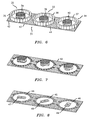
- a filter arrangement 31 includes three re-entrant resonant cavities 32 , 33 and 34 each having a cylindrical wall 35 , 36 , 37 respectively and a centrally located re-entrant stub 38 , 39 and 40 respectively.
- Each cavity also includes an end wall that is omitted in FIG. 6 for the sake of clarity.
- the cylindrical wall, stub and end wall joining them is formed as a single, metallized plastic, component fabricated by molding.
- each stub has an end face that lies in more than one plane and is non-circularly symmetrical, and they are oriented in the same direction.
- FIG. 7 is a similar view to that of FIG. 6 , except that the cylindrical walls have been omitted to reveal patterning of the metallization layer 42 more clearly.
- FIG. 9 shows only the top metal layer 42 of the substrate 41 .
- FIG. 10 illustrates the pattern of metal-filled holes 50 in the dielectric layer 43 of the substrate 41 that underlies the metallization layer 42 .
- the holes 50 connect the etched metallization layer 42 with a second metal layer 51 on the other side of the dielectric layer 43 .
- the second metal layer 51 defines part of the electrically conductive cavity surface defining the volume within which an electromagnetic field is established during operation of each cavity.
- the second metal layer 51 is continuous, as shown in FIG. 11 .
- the second metal layer 51 may include openings to allow coupling of signals into and out of the cavities.
- the PCB substrate 41 may comprise additional layers, for example, to include coupling copper traces embedded in a multilayer dielectric construction.
Landscapes
- Engineering & Computer Science (AREA)
- Manufacturing & Machinery (AREA)
- Control Of Motors That Do Not Use Commutators (AREA)
Abstract
Description
Claims (24)
Priority Applications (6)
| Application Number | Priority Date | Filing Date | Title |
|---|---|---|---|
| US11/524,111 US8324989B2 (en) | 2006-09-20 | 2006-09-20 | Re-entrant resonant cavities and method of manufacturing such cavities |
| JP2009529187A JP4833339B2 (en) | 2006-09-20 | 2007-09-10 | Reentrant resonant cavity and method for manufacturing said cavity |
| EP07838031.8A EP2092596B1 (en) | 2006-09-20 | 2007-09-10 | Re-entrant resonant cavities and method of manufacturing such cavities |
| CN2007800349190A CN101517822B (en) | 2006-09-20 | 2007-09-10 | Re-entrant resonant cavities and method of manufacturing such cavities |
| KR1020097005283A KR20090041433A (en) | 2006-09-20 | 2007-09-10 | Re-entrant resonant cavities and method of manufaturing such cavities |
| PCT/US2007/019729 WO2008036180A2 (en) | 2006-09-20 | 2007-09-10 | Re-entrant resonant cavities and method of manufacturing such cavities |
Applications Claiming Priority (1)
| Application Number | Priority Date | Filing Date | Title |
|---|---|---|---|
| US11/524,111 US8324989B2 (en) | 2006-09-20 | 2006-09-20 | Re-entrant resonant cavities and method of manufacturing such cavities |
Publications (2)
| Publication Number | Publication Date |
|---|---|
| US20080067948A1 US20080067948A1 (en) | 2008-03-20 |
| US8324989B2 true US8324989B2 (en) | 2012-12-04 |
Family
ID=39111462
Family Applications (1)
| Application Number | Title | Priority Date | Filing Date |
|---|---|---|---|
| US11/524,111 Expired - Fee Related US8324989B2 (en) | 2006-09-20 | 2006-09-20 | Re-entrant resonant cavities and method of manufacturing such cavities |
Country Status (6)
| Country | Link |
|---|---|
| US (1) | US8324989B2 (en) |
| EP (1) | EP2092596B1 (en) |
| JP (1) | JP4833339B2 (en) |
| KR (1) | KR20090041433A (en) |
| CN (1) | CN101517822B (en) |
| WO (1) | WO2008036180A2 (en) |
Cited By (1)
| Publication number | Priority date | Publication date | Assignee | Title |
|---|---|---|---|---|
| US10790565B2 (en) | 2015-08-18 | 2020-09-29 | Samsung Electronics Co., Ltd. | Cavity filter |
Families Citing this family (10)
| Publication number | Priority date | Publication date | Assignee | Title |
|---|---|---|---|---|
| US8324989B2 (en) | 2006-09-20 | 2012-12-04 | Alcatel Lucent | Re-entrant resonant cavities and method of manufacturing such cavities |
| US8333005B2 (en) * | 2009-08-10 | 2012-12-18 | James Thomas LaGrotta | Method of constructing a tunable RF filter |
| EP2337149A1 (en) | 2009-12-16 | 2011-06-22 | Alcatel Lucent | Cavity resonator |
| EP2403053B1 (en) | 2010-06-29 | 2014-11-12 | Alcatel Lucent | Coupling mechanism for a PCB mounted microwave re-entrant resonant cavity |
| US9178256B2 (en) | 2012-04-19 | 2015-11-03 | Qualcomm Mems Technologies, Inc. | Isotropically-etched cavities for evanescent-mode electromagnetic-wave cavity resonators |
| US8884725B2 (en) | 2012-04-19 | 2014-11-11 | Qualcomm Mems Technologies, Inc. | In-plane resonator structures for evanescent-mode electromagnetic-wave cavity resonators |
| US9455484B2 (en) | 2013-10-25 | 2016-09-27 | Huawei Technologies Co., Ltd. | Wideband electronically tunable cavity filters |
| WO2016023070A1 (en) * | 2014-08-12 | 2016-02-18 | The University Of Western Australia | Microwave frequency magnetic field manipulation systems and methods and associated application instruments, apparatus and system |
| JP7303063B2 (en) * | 2019-08-20 | 2023-07-04 | 日本電気株式会社 | Resonator and manufacturing method |
| WO2023130218A1 (en) * | 2022-01-04 | 2023-07-13 | Telefonaktiebolaget Lm Ericsson (Publ) | A cover and a cavity filter comprising the same |
Citations (17)
| Publication number | Priority date | Publication date | Assignee | Title |
|---|---|---|---|---|
| US2342254A (en) | 1939-07-15 | 1944-02-22 | Dallenbach Walter | Resonance device for ultra-short waves |
| GB588183A (en) | 1944-02-03 | 1947-05-15 | Patelhold Patentverwertung | Cavity resonator |
| US3733567A (en) * | 1971-04-13 | 1973-05-15 | Secr Aviation | Coaxial cavity resonator with separate controls for frequency tuning and for temperature coefficient of resonant frequency adjustment |
| US4100504A (en) * | 1977-06-20 | 1978-07-11 | Harris Corporation | Band rejection filter having integrated impedance inverter-tune cavity configuration |
| US4380747A (en) * | 1980-03-04 | 1983-04-19 | Thomson-Csf | Tunable ultra-high frequency filter with variable capacitance tuning devices |
| US4477786A (en) * | 1981-01-26 | 1984-10-16 | Toyo Communication Equipment Co., Ltd. | Semi-coaxial cavity resonator filter |
| US4890054A (en) * | 1986-12-09 | 1989-12-26 | Dipole Electronics Co., Ltd. | Apparatus and method for measuring physical quantities |
| US5285178A (en) | 1992-10-07 | 1994-02-08 | Telefonaktiebolaget L M Ericsson | Combiner resonator having an I-beam shaped element disposed within its cavity |
| US5329687A (en) | 1992-10-30 | 1994-07-19 | Teledyne Industries, Inc. | Method of forming a filter with integrally formed resonators |
| US6130189A (en) * | 1996-06-17 | 2000-10-10 | Superconductor Technologies, Inc. | Microwave hairpin-comb filters for narrow-band applications |
| US6255917B1 (en) | 1999-01-12 | 2001-07-03 | Teledyne Technologies Incorporated | Filter with stepped impedance resonators and method of making the filter |
| US6356172B1 (en) * | 1999-12-29 | 2002-03-12 | Nokia Networks Oy | Resonator structure embedded in mechanical structure |
| US6611183B1 (en) * | 1999-10-15 | 2003-08-26 | James Michael Peters | Resonant coupling elements |
| WO2004084340A1 (en) | 2003-03-18 | 2004-09-30 | Filtronic Comtek Oy | Resonator filter |
| EP1544940A1 (en) | 2003-12-19 | 2005-06-22 | Alcatel | Tower mounted amplifier filter and manufacturing method thereof |
| US6992548B2 (en) * | 2002-12-16 | 2006-01-31 | Tdk Corporation | RF module and method for arranging through holes in RF module |
| WO2008036180A2 (en) | 2006-09-20 | 2008-03-27 | Lucent Technologies Inc. | Re-entrant resonant cavities and method of manufacturing such cavities |
Family Cites Families (3)
| Publication number | Priority date | Publication date | Assignee | Title |
|---|---|---|---|---|
| JPS5535560A (en) * | 1978-09-04 | 1980-03-12 | Matsushita Electric Ind Co Ltd | Coaxial type filter |
| JPS57168505A (en) * | 1981-04-08 | 1982-10-16 | Toyo Commun Equip Co Ltd | Frequency controller of re-entrant cavity resonator |
| JP2001053512A (en) * | 1999-08-13 | 2001-02-23 | Japan Radio Co Ltd | High-frequency resonator of temperature compensating type and high-frequency filter |
-
2006
- 2006-09-20 US US11/524,111 patent/US8324989B2/en not_active Expired - Fee Related
-
2007
- 2007-09-10 EP EP07838031.8A patent/EP2092596B1/en not_active Not-in-force
- 2007-09-10 WO PCT/US2007/019729 patent/WO2008036180A2/en active Application Filing
- 2007-09-10 CN CN2007800349190A patent/CN101517822B/en not_active Expired - Fee Related
- 2007-09-10 KR KR1020097005283A patent/KR20090041433A/en not_active Application Discontinuation
- 2007-09-10 JP JP2009529187A patent/JP4833339B2/en not_active Expired - Fee Related
Patent Citations (18)
| Publication number | Priority date | Publication date | Assignee | Title |
|---|---|---|---|---|
| US2342254A (en) | 1939-07-15 | 1944-02-22 | Dallenbach Walter | Resonance device for ultra-short waves |
| GB588183A (en) | 1944-02-03 | 1947-05-15 | Patelhold Patentverwertung | Cavity resonator |
| US3733567A (en) * | 1971-04-13 | 1973-05-15 | Secr Aviation | Coaxial cavity resonator with separate controls for frequency tuning and for temperature coefficient of resonant frequency adjustment |
| US4100504A (en) * | 1977-06-20 | 1978-07-11 | Harris Corporation | Band rejection filter having integrated impedance inverter-tune cavity configuration |
| US4380747A (en) * | 1980-03-04 | 1983-04-19 | Thomson-Csf | Tunable ultra-high frequency filter with variable capacitance tuning devices |
| US4477786A (en) * | 1981-01-26 | 1984-10-16 | Toyo Communication Equipment Co., Ltd. | Semi-coaxial cavity resonator filter |
| US4890054A (en) * | 1986-12-09 | 1989-12-26 | Dipole Electronics Co., Ltd. | Apparatus and method for measuring physical quantities |
| US5285178A (en) | 1992-10-07 | 1994-02-08 | Telefonaktiebolaget L M Ericsson | Combiner resonator having an I-beam shaped element disposed within its cavity |
| US5329687A (en) | 1992-10-30 | 1994-07-19 | Teledyne Industries, Inc. | Method of forming a filter with integrally formed resonators |
| US6130189A (en) * | 1996-06-17 | 2000-10-10 | Superconductor Technologies, Inc. | Microwave hairpin-comb filters for narrow-band applications |
| US6255917B1 (en) | 1999-01-12 | 2001-07-03 | Teledyne Technologies Incorporated | Filter with stepped impedance resonators and method of making the filter |
| US6611183B1 (en) * | 1999-10-15 | 2003-08-26 | James Michael Peters | Resonant coupling elements |
| US6356172B1 (en) * | 1999-12-29 | 2002-03-12 | Nokia Networks Oy | Resonator structure embedded in mechanical structure |
| US6992548B2 (en) * | 2002-12-16 | 2006-01-31 | Tdk Corporation | RF module and method for arranging through holes in RF module |
| WO2004084340A1 (en) | 2003-03-18 | 2004-09-30 | Filtronic Comtek Oy | Resonator filter |
| US7180391B2 (en) * | 2003-03-18 | 2007-02-20 | Filtronic Comtek Oy | Resonator filter |
| EP1544940A1 (en) | 2003-12-19 | 2005-06-22 | Alcatel | Tower mounted amplifier filter and manufacturing method thereof |
| WO2008036180A2 (en) | 2006-09-20 | 2008-03-27 | Lucent Technologies Inc. | Re-entrant resonant cavities and method of manufacturing such cavities |
Non-Patent Citations (5)
| Title |
|---|
| Chi Wang et al, Modeling of Re-entrant Coaxial and Combline Resonators and Filters, 1996, IEEE, vol. 1, pp. 280-283. * |
| Definition of the word "about", www.merriam-webster.com, 2010. * |
| Lucent patent application, Hesselbarth 3, U.S. Appl. No. 11/523,998, filed Sep. 20, 2006, "Resonant Cavities and Method of Manufacturing Such Cavities". |
| Lucent patent application, Hesselbarth 4, U.S. Appl. No. 11/524,136, filed Sep. 20, 2006, "Re-Entrant Resonant Cavities, Filters Including Such Cavities and Method of Manufacture". |
| T. J. Mueller, "SMD-Type 42 GHz Waveguide Filter". Proc. IEEE Intern. Microwave Symp., Philadelphia, 2003, pp. 108901092. |
Cited By (1)
| Publication number | Priority date | Publication date | Assignee | Title |
|---|---|---|---|---|
| US10790565B2 (en) | 2015-08-18 | 2020-09-29 | Samsung Electronics Co., Ltd. | Cavity filter |
Also Published As
| Publication number | Publication date |
|---|---|
| WO2008036180A2 (en) | 2008-03-27 |
| JP2010504064A (en) | 2010-02-04 |
| CN101517822B (en) | 2013-07-10 |
| EP2092596B1 (en) | 2018-06-27 |
| KR20090041433A (en) | 2009-04-28 |
| WO2008036180A3 (en) | 2008-05-08 |
| US20080067948A1 (en) | 2008-03-20 |
| JP4833339B2 (en) | 2011-12-07 |
| EP2092596A2 (en) | 2009-08-26 |
| CN101517822A (en) | 2009-08-26 |
Similar Documents
| Publication | Publication Date | Title |
|---|---|---|
| US8324989B2 (en) | Re-entrant resonant cavities and method of manufacturing such cavities | |
| US7965251B2 (en) | Resonant cavities and method of manufacturing such cavities | |
| EP2056394B1 (en) | Cavity resonator | |
| US9887442B2 (en) | RF filter for adjusting coupling amount or transmission zero | |
| US7352264B2 (en) | Electronically tunable dielectric resonator circuits | |
| US5343176A (en) | Radio frequency filter having a substrate with recessed areas | |
| EP2070151B1 (en) | Re-entrant resonant cavities, filters including such cavities and method of manufacture | |
| Nam et al. | Low-cost high-performance frequency-tunable substrate-integrated waveguide filter structure and fabrication method | |
| WO2022199254A1 (en) | Circular filter assembly | |
| JP2007174187A (en) | Microwave oscillator | |
| Hesselbarth et al. | Dual-mode surface-mount cavity resonator and filter | |
| JPH03136402A (en) | Dielectric filter | |
| JPS63206008A (en) | Oscillator | |
| JPH07226604A (en) | Dielectric filter |
Legal Events
| Date | Code | Title | Description |
|---|---|---|---|
| AS | Assignment |
Owner name: LUCENT TECHNOLOGIES INC., NEW JERSEY Free format text: ASSIGNMENT OF ASSIGNORS INTEREST;ASSIGNOR:HESSELBARTH, JAN;REEL/FRAME:018656/0078 Effective date: 20061026 |
|
| FEPP | Fee payment procedure |
Free format text: PAYOR NUMBER ASSIGNED (ORIGINAL EVENT CODE: ASPN); ENTITY STATUS OF PATENT OWNER: LARGE ENTITY |
|
| AS | Assignment |
Owner name: ALCATEL-LUCENT USA INC., NEW JERSEY Free format text: MERGER;ASSIGNOR:LUCENT TECHNOLOGIES INC.;REEL/FRAME:027639/0138 Effective date: 20081101 |
|
| AS | Assignment |
Owner name: ALCATEL LUCENT, FRANCE Free format text: ASSIGNMENT OF ASSIGNORS INTEREST;ASSIGNOR:ALCATEL-LUCENT USA INC.;REEL/FRAME:029089/0687 Effective date: 20121004 |
|
| STCF | Information on status: patent grant |
Free format text: PATENTED CASE |
|
| AS | Assignment |
Owner name: CREDIT SUISSE AG, NEW YORK Free format text: SECURITY AGREEMENT;ASSIGNOR:LUCENT, ALCATEL;REEL/FRAME:029821/0001 Effective date: 20130130 Owner name: CREDIT SUISSE AG, NEW YORK Free format text: SECURITY AGREEMENT;ASSIGNOR:ALCATEL LUCENT;REEL/FRAME:029821/0001 Effective date: 20130130 |
|
| AS | Assignment |
Owner name: ALCATEL LUCENT, FRANCE Free format text: RELEASE BY SECURED PARTY;ASSIGNOR:CREDIT SUISSE AG;REEL/FRAME:033868/0001 Effective date: 20140819 |
|
| FPAY | Fee payment |
Year of fee payment: 4 |
|
| FEPP | Fee payment procedure |
Free format text: MAINTENANCE FEE REMINDER MAILED (ORIGINAL EVENT CODE: REM.); ENTITY STATUS OF PATENT OWNER: LARGE ENTITY |
|
| LAPS | Lapse for failure to pay maintenance fees |
Free format text: PATENT EXPIRED FOR FAILURE TO PAY MAINTENANCE FEES (ORIGINAL EVENT CODE: EXP.); ENTITY STATUS OF PATENT OWNER: LARGE ENTITY |
|
| STCH | Information on status: patent discontinuation |
Free format text: PATENT EXPIRED DUE TO NONPAYMENT OF MAINTENANCE FEES UNDER 37 CFR 1.362 |
|
| FP | Lapsed due to failure to pay maintenance fee |
Effective date: 20201204 |