US8305779B2 - Parallel-connected uninterrupted power supply circuit - Google Patents
Parallel-connected uninterrupted power supply circuit Download PDFInfo
- Publication number
- US8305779B2 US8305779B2 US12/551,042 US55104209A US8305779B2 US 8305779 B2 US8305779 B2 US 8305779B2 US 55104209 A US55104209 A US 55104209A US 8305779 B2 US8305779 B2 US 8305779B2
- Authority
- US
- United States
- Prior art keywords
- terminal
- coupled
- diode
- switch
- capacitor
- Prior art date
- Legal status (The legal status is an assumption and is not a legal conclusion. Google has not performed a legal analysis and makes no representation as to the accuracy of the status listed.)
- Active, expires
Links
- 230000007935 neutral effect Effects 0.000 claims abstract description 48
- 239000003990 capacitor Substances 0.000 claims description 104
- 238000010586 diagram Methods 0.000 description 12
- 208000015778 Undifferentiated pleomorphic sarcoma Diseases 0.000 description 8
- 238000004402 ultra-violet photoelectron spectroscopy Methods 0.000 description 8
- 238000000034 method Methods 0.000 description 5
- 230000003247 decreasing effect Effects 0.000 description 3
- 238000007599 discharging Methods 0.000 description 3
- 238000004519 manufacturing process Methods 0.000 description 3
- XEEYBQQBJWHFJM-UHFFFAOYSA-N Iron Chemical compound [Fe] XEEYBQQBJWHFJM-UHFFFAOYSA-N 0.000 description 2
- 238000005516 engineering process Methods 0.000 description 2
- 239000000463 material Substances 0.000 description 2
- 238000012986 modification Methods 0.000 description 2
- 230000004048 modification Effects 0.000 description 2
- 230000010355 oscillation Effects 0.000 description 2
- 230000009467 reduction Effects 0.000 description 2
- RYGMFSIKBFXOCR-UHFFFAOYSA-N Copper Chemical compound [Cu] RYGMFSIKBFXOCR-UHFFFAOYSA-N 0.000 description 1
- 101000668170 Homo sapiens RNA-binding motif, single-stranded-interacting protein 2 Proteins 0.000 description 1
- 102100039690 RNA-binding motif, single-stranded-interacting protein 2 Human genes 0.000 description 1
- XUIMIQQOPSSXEZ-UHFFFAOYSA-N Silicon Chemical compound [Si] XUIMIQQOPSSXEZ-UHFFFAOYSA-N 0.000 description 1
- 238000006243 chemical reaction Methods 0.000 description 1
- 229910052802 copper Inorganic materials 0.000 description 1
- 239000010949 copper Substances 0.000 description 1
- 238000012937 correction Methods 0.000 description 1
- 238000011161 development Methods 0.000 description 1
- 230000000694 effects Effects 0.000 description 1
- 238000002474 experimental method Methods 0.000 description 1
- 229910052742 iron Inorganic materials 0.000 description 1
- 230000008569 process Effects 0.000 description 1
- 238000011160 research Methods 0.000 description 1
- 229910052710 silicon Inorganic materials 0.000 description 1
- 239000010703 silicon Substances 0.000 description 1
- 238000012546 transfer Methods 0.000 description 1
Images


Classifications
-
- H—ELECTRICITY
- H02—GENERATION; CONVERSION OR DISTRIBUTION OF ELECTRIC POWER
- H02J—CIRCUIT ARRANGEMENTS OR SYSTEMS FOR SUPPLYING OR DISTRIBUTING ELECTRIC POWER; SYSTEMS FOR STORING ELECTRIC ENERGY
- H02J9/00—Circuit arrangements for emergency or stand-by power supply, e.g. for emergency lighting
- H02J9/04—Circuit arrangements for emergency or stand-by power supply, e.g. for emergency lighting in which the distribution system is disconnected from the normal source and connected to a standby source
- H02J9/06—Circuit arrangements for emergency or stand-by power supply, e.g. for emergency lighting in which the distribution system is disconnected from the normal source and connected to a standby source with automatic change-over, e.g. UPS systems
- H02J9/062—Circuit arrangements for emergency or stand-by power supply, e.g. for emergency lighting in which the distribution system is disconnected from the normal source and connected to a standby source with automatic change-over, e.g. UPS systems for AC powered loads
- H02J9/063—Common neutral, e.g. AC input neutral line connected to AC output neutral line and DC middle point
-
- Y—GENERAL TAGGING OF NEW TECHNOLOGICAL DEVELOPMENTS; GENERAL TAGGING OF CROSS-SECTIONAL TECHNOLOGIES SPANNING OVER SEVERAL SECTIONS OF THE IPC; TECHNICAL SUBJECTS COVERED BY FORMER USPC CROSS-REFERENCE ART COLLECTIONS [XRACs] AND DIGESTS
- Y02—TECHNOLOGIES OR APPLICATIONS FOR MITIGATION OR ADAPTATION AGAINST CLIMATE CHANGE
- Y02P—CLIMATE CHANGE MITIGATION TECHNOLOGIES IN THE PRODUCTION OR PROCESSING OF GOODS
- Y02P80/00—Climate change mitigation technologies for sector-wide applications
- Y02P80/10—Efficient use of energy, e.g. using compressed air or pressurized fluid as energy carrier
Definitions
- the present invention relates to a parallel-connected uninterrupted power supply (UPS) circuit. More particularly, it relates to a circuit having a plurality of UPSs parallel-connected to each other such that the plurality of UPSs could reach a current balance.
- UPS uninterrupted power supply
- FIG. 1 shows a circuit diagram of a conventional online UPS.
- a power factor correction (PFC) boost converter including silicon-controlled rectifiers (SCRs) SCR 1 -SCR 2 , inductors L 1 -L 2 , switches S 1 -S 2 , diodes D 1 -D 2 and capacitors C 1 -C 2 ), an inverter (including switches Si 1 -Si 2 , inductor Li and output capacitor Co), a controller (not shown) and a battery set (including a battery having a positive terminal and a negative terminal, SCRs SCR 3 -SCR 4 and a fuse F 2 ), and it further includes an input electrical magnetic interference (EMI) filter having a bypass AC input terminal, a normal AC input terminal and a neutral input terminal, fuses F 1 and F 3 , inductor Lf, SCRs SCR 5 -SCR 8 and an output EMI filter.
- PFC power factor correction
- EMI input electrical magnetic interference
- a rectifying circuit of the PFC boost converter is usually connected to the front-end of the battery and includes two rectifying switches. Please refer to the two SCRs SCR 1 -SCR 2 of FIG. 1 .
- the choice for a conventional PFC circuit is usually a three-level PFC circuit, which includes an upper boost circuit providing a voltage to the positive DC bus capacitor C 1 and a lower boost circuit providing a voltage to the negative DC bus capacitor C 2 .
- the three-level PFC circuit is jointly used by the AC mode when the conventional online UPS as shown in FIG. 1 is operating under the DC mode, and please refer to FIGS. 2( a )- 2 ( b ) for the specific working processes.
- FIG. 2( a ) shows current flow directions of the positive half-cycle of the DC mode when the conventional online UPS is working under the DC mode.
- the smaller dashed path in the central portion of FIG. 2( a ) shows a current charging the inductors L 1 and L 2 .
- the larger dashed path in the surrounding portion of FIG. 2( a ) shows a continued current of inductor charging the capacitor C 1 .
- FIG. 2( b ) shows current flow directions when the conventional online UPS is working under the negative half-cycle of the DC mode.
- the smaller dashed path in the central portion of FIG. 2( b ) shows a current charging the inductors L 1 and L 2 .
- the larger dashed path in the surrounding portion of FIG. 2( b ) shows a continued current of inductor charging the capacitor C 2 . As shown in FIG.
- the lower switch S 2 is continuously turned on and the upper switch S 1 is engaged in the pulse-width modulation (PWM) chopping when a voltage is provided to the capacitor C 1 connected to the positive terminal of DC bus in the positive half-cycle
- the upper switch S 1 is continuously turned on and the lower switch S 2 is engaged in the PWM chopping when a voltage is provided to the capacitor C 2 connected to the negative terminal of DC bus in the negative half-cycle.
- the input terminals of the UPS include an I/L and a neutral I/N, and the neutral should go straightly through the whole UPS until reaching the load side and connect to one of the two terminals of the load (O/L and O/N) from the reliability point of view.
- the positive and the negative terminals of the battery are connected to the neutral through the inductors L 1 and L 2 when the above-mentioned conventional online UPS is in a battery mode, thus the voltage on the neutral generates a voltage jump while switching and results in a quite large EMI.
- the two bypass diodes (DP and DN) connected in series and in front of the two inductors (L 1 and L 2 ), and the middle point of the two bypass diodes (DP and DN) is coupled to the neutral I/N.
- switches S 1 and S 2 are under high frequency switching, one of the two inductors is failed, the EMI problem is greatly improved.
- the inductors of the PFC circuit alternately work under working frequency such that the utilization rate of the inductors is only 50% when the conventional online UPS operates under the battery mode.
- the current sharing of the two inductors L 1 s through the parallel-connected circuit configured by the neutral is also determined by the parameters of L 1 s .
- the parameters of inductors L 1 and L 2 are related to the manufacturing technologies and the materials, and are hard to achieve basically the same.
- the magnetic elements such as the inductors are manufactured by mine materials containing copper and iron, and the costs of which are increasingly higher following the development of the economy. In this way, the currents flow through the inductors of each UPS mode are hardly to be independently controlled, which causes the input power of each UPS to be different from each other, result in inductor current oscillations and the current unbalance of switches, and the single battery set parallel-connected to multiple UPSs can not be realized also.
- a UPS circuit includes a neutral, a battery having a positive terminal receiving a first DC voltage and a negative terminal, a first PFC boost converter including a first PFC circuit outputting a second and a third DC voltages, and including a first inductor having a first terminal coupled to the positive terminal and a second terminal, a first rectifying bridge including a first and a second bypass diodes coupled to a first middle point coupled to the second terminal of the first inductor, and having a first terminal and a second terminal coupled to the negative terminal, a first switch bridge including a first upper and a first lower switches coupled to a second middle point, and having a first terminal coupled to the first terminal of the first rectifying bridge and a second terminal coupled to the second terminal of the first rectifying bridge, a first control switch having a first terminal coupled to the second middle point, a second terminal coupled to the neutral and a control terminal, and a first inverter receiving the second and the third DC voltages and outputting a first
- the circuit further includes a rectifying circuit, an output capacitor having a first and a second terminals and a DC bus having a positive and a negative terminals, wherein each of the first and the second control switches further includes a control terminal, the rectifying circuit receives a second AC voltage and outputs the first DC voltage, each of the first and the second inverters has a first input terminal coupled to the positive terminal of the DC bus, a second input terminal coupled to the negative terminal of the DC bus and an output terminal coupled to the first terminal of the output capacitor, and the neutral is coupled to the second terminal of the output capacitor.
- the first PFC circuit further includes a first upper diode, a first upper capacitor, a first lower diode and a first lower capacitor
- the second PFC circuit further comprises a second upper diode, a second upper capacitor, a second lower diode and a second lower capacitor, each the diode has an anode and a cathode, and each the capacitor has a first and a second terminals.
- the anode of the first upper diode is coupled to the first terminal of the first switch bridge
- the cathode of the first upper diode is coupled to the first terminal of the first upper capacitor and the first input terminal of the first inverter
- the cathode of the first lower diode is coupled to the second terminal of the first switch bridge
- the anode of the first lower diode is coupled to the second terminal of the first lower capacitor and the second input terminal of the first inverter
- the second terminal of the first upper capacitor and the first terminal of the first lower capacitor are both coupled to the neutral
- the anode of the second upper diode is coupled to the first terminal of the second switch bridge
- the cathode of the second upper diode is coupled to the first terminal of the second upper capacitor and the first input terminal of the second inverter
- the cathode of the second lower diode is coupled to the second terminal of the second switch bridge
- the anode of the second lower diode is coupled to the second terminal of the second lower capacitor and the
- the anode of the first upper diode is coupled to the second terminal of the first inductor
- the first bypass diode is a first SCR
- the anode of the first SCR is coupled to the anode of the first upper diode
- the cathode of the first SCR is coupled to the drain of the first upper switch
- the anode of the second upper diode is coupled to the second terminal of the second inductor
- the third bypass diode is a second SCR
- the anode of the second SCR is coupled to the anode of the second upper diode
- the cathode of the second SCR is coupled to the drain of the second upper switch
- the first PFC circuit further includes a first upper diode, a first upper capacitor, a third control switch and a first lower capacitor
- the second PFC circuit further comprises a second upper diode, a second upper capacitor, a fourth control switch and a second lower capacitor
- each the diode has an anode and a cathode
- each the capacitor has a first and a second terminals
- each of the third and the fourth control switches has a first, a second and a control terminals.
- the anode of the first upper diode is coupled to the first terminal of the first switch bridge
- the cathode of the first upper diode is coupled to the first terminal of the first upper capacitor and the first input terminal of the first inverter
- the second terminal of the third control switch is coupled to the second terminal of the first switch bridge
- the first terminal of the third control switch is coupled to the second terminal of the first lower capacitor and the second input terminal of the first inverter
- the second terminal of the first upper capacitor and the first terminal of the first lower capacitor are both coupled to the neutral
- the anode of the second upper diode is coupled to the first terminal of the second switch bridge
- the cathode of the second upper diode is coupled to the first terminal of the second upper capacitor and the first input terminal of the second inverter
- the second terminal of the fourth control switch is coupled to the second terminal of the second switch bridge
- the first terminal of the fourth control switch is coupled to the second terminal of the second lower capacitor and the second input terminal of the second inverter
- the third control switch is an IGBT having a reverse parallel-connected diode
- the fourth control switch is an IGBT having a reverse parallel-connected diode
- each of the first upper and the first lower switches has a first, a second and a control terminals, the first terminal of the first upper switch and the second terminal of the first lower switch are both coupled to the second middle point, the second terminal of the first upper switch is coupled to the first terminal of the first switch bridge, and the first terminal of the first lower switch is coupled to the second terminal of the first switch bridge.
- each of the second upper and the second lower switches has a first, a second and a control terminals, the first terminal of the second upper switch and the second terminal of the second lower switch are both coupled to the fourth middle point, the second terminal of the second upper switch is coupled to the first terminal of the second switch bridge, and the first terminal of the second lower switch is coupled to the second terminal of the second switch bridge.
- each the diode has an anode and a cathode
- the anode of the first bypass diode is coupled to the cathode of the second bypass diode and the first middle point
- the cathode of the first bypass diode is coupled to the first terminal of the first rectifying bridge
- the anode of the second bypass diode is coupled to the second terminal of the first rectifying bridge.
- each the diode has an anode and a cathode
- the anode of the third bypass diode is coupled to the cathode of the fourth bypass diode and the third middle point
- the cathode of the third bypass diode is coupled to the first terminal of the second rectifying bridge
- the anode of the fourth bypass diode is coupled to the second terminal of the second rectifying bridge.
- the circuit operates under one of a DC mode having a positive and a negative half-cycles and an AC mode having a positive and a negative half-cycles, wherein each of the first and the second control switches is an IGBT having a reverse parallel-connected diode, the first and the second control switches are turned on while under the positive half-cycle of the DC mode and the positive and the negative half-cycle of the AC mode; the first and the second control switches are turned off while under the negative half-cycle of the DC mode where the reverse parallel-connected diodes of the first and the second control switches are respectively used to prevent reverse flows of a first current of the first control switch and a second current of the second control switch and to bear a first reverse and a second reverse voltages such that the first and the second PFC circuits reach a current balance at this time moment.
- each of the first and the second control switches is an IGBT having a reverse parallel-connected diode
- the first and the second control switches are turned on while under the positive half-cycle of the DC mode and the positive and
- a UPS circuit includes a neutral, a battery having a positive terminal receiving a first DC voltage and a negative terminal, and a plurality of PFC boost converters, each of which includes a PFC circuit outputting a second and a third DC voltages
- an inductor having a first terminal coupled to the positive terminal and a second terminal
- a rectifying bridge includes a first and a second bypass diodes coupled to a first middle point coupled to the second terminal of the inductor, and having a first terminal and a second terminal coupled to the negative terminal
- a switch bridge includes a first upper and a first lower switches coupled to a second middle point, and having a first terminal coupled to the first terminal of the rectifying bridge and a second terminal coupled to the second terminal of the rectifying bridge
- a control switch having a first terminal coupled to the second middle point and a second terminal coupled to the neutral, and an inverter receiving the second and the third DC voltages and outputting a first AC voltage.
- the circuit further includes a rectifying circuit, an output capacitor having a first and a second terminals and a DC bus having a positive and a negative terminals
- each the control switch further includes a control terminal
- the rectifying circuit receives a second AC voltage and outputs the first DC voltage
- each the inverter has a first input terminal coupled to the positive terminal of the DC bus, a second input terminal coupled to the negative terminal of the DC bus and an output terminal coupled to the first terminal of the output capacitor, and the neutral is coupled to the second terminal of the output capacitor.
- each the PFC circuit further includes an upper diode, an upper capacitor, a lower diode and a lower capacitor, each the diode has an anode and a cathode, each the capacitor has a first and a second terminals, the anode of the upper diode is coupled to the first terminal of the switch bridge, the cathode of the upper diode is coupled to the first terminal of the upper capacitor and the first input terminal of the inverter, the cathode of the lower diode is coupled to the second terminal of the switch bridge, the anode of the lower diode is coupled to the second terminal of the lower capacitor and the second input terminal of the inverter, and the second terminal of the upper capacitor and the first terminal of the lower capacitor are both coupled to the neutral.
- each the PFC circuit further includes an upper diode, an upper capacitor, an EMI control switch and a lower capacitor, each the diode has an anode and a cathode, each the capacitor has a first and a second terminals, the EMI control switch has a first, a second and a control terminals, the anode of the upper diode is coupled to the first terminal of the switch bridge, the cathode of the upper diode is coupled to the first terminal of the upper capacitor and the first input terminal of the inverter, the second terminal of the EMI control switch is coupled to the second terminal of the switch bridge, the first terminal of the EMI control switch is coupled to the second terminal of the lower capacitor and the second input terminal of the inverter, and the second terminal of the upper capacitor and the first terminal of the lower capacitor are both coupled to the neutral.
- each of the upper and the lower switches has a first, a second and a control terminals, the first terminal of the upper switch and the second terminal of the lower switch are both coupled to the second middle point, the second terminal of the upper switch is coupled to the first terminal of the switch bridge, and the first terminal of the lower switch is coupled to the second terminal of the switch bridge.
- each the diode has an anode and a cathode
- the anode of the first bypass diode is coupled to the cathode of the second bypass diode and the first middle point
- the cathode of the first bypass diode is coupled to the first terminal of the rectifying bridge
- the anode of the second bypass diode is coupled to the second terminal of the rectifying bridge.
- the circuit operates under one of a DC mode having a positive and a negative half-cycles and an AC mode having a positive and a negative half-cycles
- the control switch is an IGBT having a reverse parallel-connected diode
- the control switch is turned on while under the positive half-cycle of one of the DC mode and the positive and the negative half-cycle of AC mode
- the control switch is turned off while under the negative half-cycle of the DC mode where the reverse parallel-connected diode of the control switch is used to prevent a reverse flow of a current of the control switch and to bear a reverse voltage such that all the PFC circuits reach a current balance at this time moment.
- a UPS circuit includes a neutral, a battery having a positive terminal receiving a first DC voltage and a negative terminal, and a first PFC boost converter including a first PFC circuit outputting a second and a third DC voltages, and including a first inductor having a first terminal coupled to the positive terminal and a second terminal, a first rectifying bridge including a first and a second bypass diodes coupled to a first middle point coupled to the second terminal of the first inductor, and having a first terminal and a second terminal coupled to the negative terminal, a first switch bridge including a first upper and a first lower switches coupled to a second middle point, and having a first terminal coupled to the first terminal of the first rectifying bridge and a second terminal coupled to the second terminal of the first rectifying bridge, a first control switch having a first terminal coupled to the second middle point and a second terminal coupled to the neutral, and a first inverter receiving the second and the third DC voltages and outputting a first AC voltage.
- the circuit further includes a second PFC boost converter, wherein each of the first and the second control switches further includes a control terminal.
- FIG. 1 shows a circuit diagram of an online UPS in the prior art
- FIG. 2( a ) shows current flow directions in the positive half-cycle of the DC mode of the online UPS as shown in FIG. 1 ;
- FIG. 2( b ) shows current flow directions in the negative half-cycle of the DC mode of the online UPS as shown in FIG. 1 ;
- FIG. 2( c ) shows waveform diagrams of the output voltage and the driving signals of the upper and the lower switches in the positive and the negative half-cycles of the DC mode of the online UPS as shown in FIG. 1 ;
- FIG. 2( d ) shows a circuit diagram of another online UPS in the prior art
- FIG. 3 shows a circuit diagram of an online UPS according to the first preferred embodiment of the present invention
- FIG. 4 shows a circuit diagram of an online parallel-connected UPS circuit according to the second preferred embodiment of the present invention
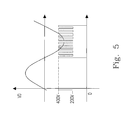
- FIG. 5 shows waveform diagrams displaying high-frequency voltage jump EMI when an inductor of the online UPS as shown in FIG. 4 is charging and discharging;
- FIG. 6 shows a circuit diagram of an online UPS according to the third preferred embodiment of the present invention.
- FIG. 7 shows a circuit diagram of an online UPS according to the fourth preferred embodiment of the present invention.
- FIG. 3 shows a circuit diagram of an online UPS according to the first preferred embodiment of the present invention.
- an inductor Lp used for the PFC and connected before the rectifying bridge of DP and DN, and after the battery.
- this inductor Lp is used to engage the conversion no matter it is in the positive half-cycle or the negative half-cycle of the input voltage.
- the UPS enters the DC (battery) mode when the AC is cut off, and the positive terminal of the battery set goes through a SCR SCR 3 and connects to the front-end of PFC inductor Lp.
- the AC switch In the DC mode, the AC switch is turned off, and the battery set goes through the jointly used PFC circuit to transfer the energy to the positive/negative terminals of the DC bus for providing the power to the inverter 3 .
- the negative terminal of the battery set goes through a SCR SCR 4 to be connected to the lower switch S 2 of the PFC circuit.
- each parallel-connected UPS mode could independently control the current it draws from the jointly used battery. That is to say, the input current of each UPS can be controlled independently but not to generate the problems such as current unbalance among power modes and current oscillations due to that the circuit of the jointly used battery is connected.
- the method employed in the present invention is to add an IGBT having a reverse parallel-connected diode (S 3 as shown in FIG. 3 ) among the neutral and the PFC switches such that there is a controllable decoupling switch S 3 between the negative terminal of the battery set and the neutral.
- FIG. 6 a circuit diagram of an online UPS according to the third preferred embodiment of the present invention is shown in FIG. 6 .
- a switch S 4 is parallel-connected to the originally configured diode D 2 , and S 4 is turned on only in the negative half-cycle of the DC mode, thus to keep the voltage at the cathode terminal of D 2 at ⁇ 400V no matter it is in the aforementioned inductor charging stage or the inductor discharging stage.
- D 1 is a diode which could bear a high voltage of 800V as shown in FIG. 6 , thus in the circuit according to the fourth preferred embodiment of the present invention as shown in FIG.
- the anode of D 1 is directly connected to the PFC inductor LP, a SCR SCR 9 is used to replace DP at the same time, the anode of SCR 9 is coupled to the anode of D 1 , and the cathode of SCR 9 is coupled to the drain of S 1 . In this way, the conduction loss of SCR 9 is decreased, and the various working statuses of the circuit are not influenced.
- the utilization rate of the inductor is raised, and the price of an inductor is far higher than that of the increased control (decoupling) switch S 3 , thus the cost is also lowered by the present invention.
- a decoupling switch S 3 in the present invention a battery set could be jointly used by multiple UPS modes and there is nothing to worry about the current balance problem, and the EMI problem is solved by adding a switch S 4 .
- certain conduction losses of SCR 9 are saved through connecting the anode of D 1 to the PFC inductor LP and using a SCR SCR 9 to replace DP.
- the present invention accomplishes the original functions on the basis of cost reduction, and the parallel connection of multiple UPS modes is realized.
- the present invention provides a parallel-connected UPS circuit, and this circuit realizes the multiple UPS modes parallel-connected to a battery set, causes all the UPS modes to reach a current balance and reduces the usage of magnetic elements while comparing to the conventional configuration thus to dramatically decrease the volume of the UPS power mode, greatly diminish the EMI, relatively decrease the manufacturing costs and the total costs of the parallel-connected UPS circuit at the same time due to that an inductor is decreased and a switch is increased in each of the UPS modes.
Landscapes
- Business, Economics & Management (AREA)
- Emergency Management (AREA)
- Engineering & Computer Science (AREA)
- Power Engineering (AREA)
- Rectifiers (AREA)
Abstract
Description
Claims (22)
Applications Claiming Priority (3)
| Application Number | Priority Date | Filing Date | Title |
|---|---|---|---|
| TW97133516 | 2008-09-01 | ||
| TW097133516A TWI367619B (en) | 2008-09-01 | 2008-09-01 | Parallel-connectred uninterrupted power supply circuit |
| TW97133516A | 2008-09-01 |
Publications (2)
| Publication Number | Publication Date |
|---|---|
| US20100054002A1 US20100054002A1 (en) | 2010-03-04 |
| US8305779B2 true US8305779B2 (en) | 2012-11-06 |
Family
ID=41725230
Family Applications (1)
| Application Number | Title | Priority Date | Filing Date |
|---|---|---|---|
| US12/551,042 Active 2031-03-22 US8305779B2 (en) | 2008-09-01 | 2009-08-31 | Parallel-connected uninterrupted power supply circuit |
Country Status (2)
| Country | Link |
|---|---|
| US (1) | US8305779B2 (en) |
| TW (1) | TWI367619B (en) |
Cited By (5)
| Publication number | Priority date | Publication date | Assignee | Title |
|---|---|---|---|---|
| US20110273159A1 (en) * | 2010-05-07 | 2011-11-10 | Mitsubishi Electric Corporation | Power conversion circuit |
| US20120175958A1 (en) * | 2011-01-11 | 2012-07-12 | American Power Conversion Corporation | Method and apparatus for providing uninterruptible power |
| US20130049699A1 (en) * | 2011-08-29 | 2013-02-28 | American Power Conversion Corporation | Twin boost converter with integrated charger for ups system |
| US20160276949A1 (en) * | 2015-03-20 | 2016-09-22 | Hubbell Incorporated | Universal input electronic transformer |
| TWI755290B (en) * | 2020-03-03 | 2022-02-11 | 台達電子工業股份有限公司 | Method for operating power factor correction circuit and method for operating uninterruptible power supply apparatus |
Families Citing this family (23)
| Publication number | Priority date | Publication date | Assignee | Title |
|---|---|---|---|---|
| US8492928B2 (en) * | 2010-03-18 | 2013-07-23 | American Power Conversion Corporation | AC-to-DC conversion |
| CN101807804B (en) * | 2010-03-19 | 2012-07-04 | 艾默生网络能源有限公司 | Uninterrupted power supply system with shared battery |
| CN101931337B (en) * | 2010-09-09 | 2012-07-11 | 西安交通大学 | Chopper inverter circuit for photovoltaic power generation and control method thereof |
| CN102545658B (en) * | 2010-12-21 | 2015-03-18 | 广东易事特电源股份有限公司 | Input rectifying circuit of auxiliary power supply |
| US8513928B2 (en) * | 2011-01-05 | 2013-08-20 | Eaton Corporation | Bidirectional buck-boost converter |
| US9024476B2 (en) * | 2011-07-28 | 2015-05-05 | Schneider Electric It Corporation | Single-battery power topologies for online UPS systems |
| US9065277B1 (en) | 2012-02-29 | 2015-06-23 | Google Inc. | Battery backup system for uninterrupted power supply |
| JP5403090B2 (en) * | 2012-03-09 | 2014-01-29 | 富士電機株式会社 | Power converter |
| JP5370519B2 (en) * | 2012-03-15 | 2013-12-18 | 富士電機株式会社 | Power converter |
| US9362781B2 (en) | 2012-09-14 | 2016-06-07 | Chloride Srl | Uninterruptible power supply system with fast transfer for undervoltage source line failures |
| US9931947B2 (en) * | 2013-08-30 | 2018-04-03 | Infineon Technologies Ag | Charging a capacitor |
| CN106170916A (en) * | 2014-02-07 | 2016-11-30 | Abb 瑞士股份有限公司 | There is the uninterrupted power source of balance buck/boost changer |
| CN108462390B (en) * | 2017-02-17 | 2021-03-16 | 亚瑞源科技(深圳)有限公司 | Boosting module for uninterruptible power system |
| US10811987B2 (en) * | 2017-03-31 | 2020-10-20 | Schneider Electric It Corporation | Bi-directional DC-DC converter with load and source synchronized power control |
| TWI658678B (en) * | 2017-12-25 | 2019-05-01 | 台達電子工業股份有限公司 | Uninterruptible power supply apparatus |
| CN111327194B (en) * | 2018-12-13 | 2021-08-06 | 台达电子工业股份有限公司 | Power converter and power supply device sharing direct-current power supply |
| CN111478423A (en) * | 2019-01-23 | 2020-07-31 | 日月元科技(深圳)有限公司 | Improved power supply circuit |
| US11088615B2 (en) * | 2019-08-23 | 2021-08-10 | Eaton Intelligent Power Limited | Balancing multilevel DC-DC converter apparatus |
| TWI708472B (en) * | 2020-03-31 | 2020-10-21 | 義守大學 | Converter |
| CN212210538U (en) * | 2020-05-22 | 2020-12-22 | 广州视源电子科技股份有限公司 | Three-bridge-arm topology device and uninterruptible power supply system |
| CN111668918A (en) * | 2020-06-11 | 2020-09-15 | 浪潮电子信息产业股份有限公司 | Dual-power switching method, system and device of server and readable storage medium |
| CN114069819A (en) * | 2020-08-07 | 2022-02-18 | 台达电子工业股份有限公司 | Conversion device with three-layer switching circuit and operation method of three-layer switching circuit |
| TWI777589B (en) * | 2021-06-03 | 2022-09-11 | 西勝國際股份有限公司 | Power supply system with mechanism of preventing battery packs connected in parallel from charging to each other |
Citations (4)
| Publication number | Priority date | Publication date | Assignee | Title |
|---|---|---|---|---|
| US4635177A (en) * | 1984-11-16 | 1987-01-06 | Sundstrand Corporation | Control for a neutral point clamped PWM inverter |
| US7075193B2 (en) * | 2002-02-01 | 2006-07-11 | Emerson Network Power Co., Ltd. | Power factor correcting circuit for uninterrupted power supply |
| US7450408B2 (en) * | 2005-07-26 | 2008-11-11 | Delta Electronics, Inc. | Integrated converter having three-phase power factor correction |
| US7579714B2 (en) * | 2004-12-10 | 2009-08-25 | Sanyo Denki Co., Ltd. | Uninterruptible power supply apparatus |
-
2008
- 2008-09-01 TW TW097133516A patent/TWI367619B/en active
-
2009
- 2009-08-31 US US12/551,042 patent/US8305779B2/en active Active
Patent Citations (4)
| Publication number | Priority date | Publication date | Assignee | Title |
|---|---|---|---|---|
| US4635177A (en) * | 1984-11-16 | 1987-01-06 | Sundstrand Corporation | Control for a neutral point clamped PWM inverter |
| US7075193B2 (en) * | 2002-02-01 | 2006-07-11 | Emerson Network Power Co., Ltd. | Power factor correcting circuit for uninterrupted power supply |
| US7579714B2 (en) * | 2004-12-10 | 2009-08-25 | Sanyo Denki Co., Ltd. | Uninterruptible power supply apparatus |
| US7450408B2 (en) * | 2005-07-26 | 2008-11-11 | Delta Electronics, Inc. | Integrated converter having three-phase power factor correction |
Cited By (12)
| Publication number | Priority date | Publication date | Assignee | Title |
|---|---|---|---|---|
| US20110273159A1 (en) * | 2010-05-07 | 2011-11-10 | Mitsubishi Electric Corporation | Power conversion circuit |
| US8716986B2 (en) * | 2010-05-07 | 2014-05-06 | Mitsubishi Electric Corporation | Power conversion circuit |
| US9065357B2 (en) | 2010-05-07 | 2015-06-23 | Mitsubishi Electric Corporation | Power conversion circuit |
| US20120175958A1 (en) * | 2011-01-11 | 2012-07-12 | American Power Conversion Corporation | Method and apparatus for providing uninterruptible power |
| US8878389B2 (en) * | 2011-01-11 | 2014-11-04 | Schneider Electric It Corporation | Method and apparatus for providing uninterruptible power |
| US20130049699A1 (en) * | 2011-08-29 | 2013-02-28 | American Power Conversion Corporation | Twin boost converter with integrated charger for ups system |
| US8884464B2 (en) * | 2011-08-29 | 2014-11-11 | Schneider Electric It Corporation | Twin boost converter with integrated charger for UPS system |
| US20160276949A1 (en) * | 2015-03-20 | 2016-09-22 | Hubbell Incorporated | Universal input electronic transformer |
| US10361637B2 (en) * | 2015-03-20 | 2019-07-23 | Hubbell Incorporated | Universal input electronic transformer |
| US20190348922A1 (en) * | 2015-03-20 | 2019-11-14 | Hubbell Incorporated | Universal input electronic transformer |
| US11557977B2 (en) | 2015-03-20 | 2023-01-17 | Hubbell Lighting, Inc. | Universal input electronic transformer |
| TWI755290B (en) * | 2020-03-03 | 2022-02-11 | 台達電子工業股份有限公司 | Method for operating power factor correction circuit and method for operating uninterruptible power supply apparatus |
Also Published As
| Publication number | Publication date |
|---|---|
| US20100054002A1 (en) | 2010-03-04 |
| TWI367619B (en) | 2012-07-01 |
| TW201012028A (en) | 2010-03-16 |
Similar Documents
| Publication | Publication Date | Title |
|---|---|---|
| US8305779B2 (en) | Parallel-connected uninterrupted power supply circuit | |
| US8736238B2 (en) | Buck and buck/boost converter systems having auxiliary circuits and method thereof | |
| US7005759B2 (en) | Integrated converter having three-phase power factor correction | |
| US8957542B2 (en) | Non-isolated AC-DC converter having a positive output buck-boost converter and PFC at input supply | |
| US8946931B2 (en) | Dual boost converter for UPS system | |
| US8008809B2 (en) | 3-phase high power UPS | |
| US8884464B2 (en) | Twin boost converter with integrated charger for UPS system | |
| US7729139B2 (en) | Current source inverter with energy clamp circuit and controlling method thereof having relatively better effectiveness | |
| US7009852B2 (en) | DC-DC converter circuits and method for reducing DC bus capacitor current | |
| US7888819B2 (en) | Multi-input power converter and uninterruptible power supply having the same | |
| US7514817B2 (en) | Converting device with power factor correcting and dc/dc converting functions | |
| US20060175904A1 (en) | Ups having a dual-use boost converter | |
| CN107785987B (en) | Online uninterrupted power supply | |
| Siwakoti et al. | Power electronics converters—An overview | |
| JP4951476B2 (en) | Uninterruptible power system | |
| US7710087B2 (en) | Power converter and power converting method | |
| de Paula et al. | An extensive review of nonisolated DC-DC boost-based converters | |
| CN100377481C (en) | Integration converton with three phase power factor correction | |
| US20230253877A1 (en) | Power factor correction and dc-dc multiplexing converter and uninterruptible power supply including the same | |
| Aamir et al. | Non-isolated single phase uninterruptible power supply (UPS) system | |
| CN107615634B (en) | Power conversion device and power supply system using same | |
| CN111327194B (en) | Power converter and power supply device sharing direct-current power supply | |
| TW201806297A (en) | Power factor correction circuit and corrector thereof | |
| Li et al. | A single-phase single-stage AC-DC stacked flyback converter with active clamp ZVS | |
| JP3495295B2 (en) | DC-DC converter |
Legal Events
| Date | Code | Title | Description |
|---|---|---|---|
| AS | Assignment |
Owner name: DELTA ELECTRONICS, INC.,TAIWAN Free format text: ASSIGNMENT OF ASSIGNORS INTEREST;ASSIGNORS:LU, YANSONG;TAN, JINGTAO;CHEN, XIAO;AND OTHERS;REEL/FRAME:023172/0357 Effective date: 20090828 Owner name: DELTA ELECTRONICS, INC., TAIWAN Free format text: ASSIGNMENT OF ASSIGNORS INTEREST;ASSIGNORS:LU, YANSONG;TAN, JINGTAO;CHEN, XIAO;AND OTHERS;REEL/FRAME:023172/0357 Effective date: 20090828 |
|
| STCF | Information on status: patent grant |
Free format text: PATENTED CASE |
|
| FPAY | Fee payment |
Year of fee payment: 4 |
|
| MAFP | Maintenance fee payment |
Free format text: PAYMENT OF MAINTENANCE FEE, 8TH YEAR, LARGE ENTITY (ORIGINAL EVENT CODE: M1552); ENTITY STATUS OF PATENT OWNER: LARGE ENTITY Year of fee payment: 8 |
|
| MAFP | Maintenance fee payment |
Free format text: PAYMENT OF MAINTENANCE FEE, 12TH YEAR, LARGE ENTITY (ORIGINAL EVENT CODE: M1553); ENTITY STATUS OF PATENT OWNER: LARGE ENTITY Year of fee payment: 12 |