US8258020B2 - Interconnects for stacked non-volatile memory device and method - Google Patents
Interconnects for stacked non-volatile memory device and method Download PDFInfo
- Publication number
- US8258020B2 US8258020B2 US12/939,824 US93982410A US8258020B2 US 8258020 B2 US8258020 B2 US 8258020B2 US 93982410 A US93982410 A US 93982410A US 8258020 B2 US8258020 B2 US 8258020B2
- Authority
- US
- United States
- Prior art keywords
- wiring structure
- array
- region
- dielectric material
- devices
- Prior art date
- Legal status (The legal status is an assumption and is not a legal conclusion. Google has not performed a legal analysis and makes no representation as to the accuracy of the status listed.)
- Active, expires
Links
- 238000000034 method Methods 0.000 title claims abstract description 85
- 239000000463 material Substances 0.000 claims abstract description 71
- 239000003989 dielectric material Substances 0.000 claims abstract description 59
- 239000000758 substrate Substances 0.000 claims abstract description 51
- 230000002093 peripheral effect Effects 0.000 claims abstract description 46
- 229910052709 silver Inorganic materials 0.000 claims description 13
- 239000004332 silver Substances 0.000 claims description 13
- 229910052782 aluminium Inorganic materials 0.000 claims description 12
- XAGFODPZIPBFFR-UHFFFAOYSA-N aluminium Chemical compound [Al] XAGFODPZIPBFFR-UHFFFAOYSA-N 0.000 claims description 12
- RYGMFSIKBFXOCR-UHFFFAOYSA-N Copper Chemical compound [Cu] RYGMFSIKBFXOCR-UHFFFAOYSA-N 0.000 claims description 9
- BQCADISMDOOEFD-UHFFFAOYSA-N Silver Chemical compound [Ag] BQCADISMDOOEFD-UHFFFAOYSA-N 0.000 claims description 9
- 229910052802 copper Inorganic materials 0.000 claims description 9
- 239000010949 copper Substances 0.000 claims description 9
- 229910052721 tungsten Inorganic materials 0.000 claims description 9
- 239000010937 tungsten Substances 0.000 claims description 9
- WFKWXMTUELFFGS-UHFFFAOYSA-N tungsten Chemical compound [W] WFKWXMTUELFFGS-UHFFFAOYSA-N 0.000 claims description 8
- 239000007769 metal material Substances 0.000 claims description 7
- PXHVJJICTQNCMI-UHFFFAOYSA-N Nickel Chemical compound [Ni] PXHVJJICTQNCMI-UHFFFAOYSA-N 0.000 claims description 6
- BASFCYQUMIYNBI-UHFFFAOYSA-N platinum Chemical compound [Pt] BASFCYQUMIYNBI-UHFFFAOYSA-N 0.000 claims description 6
- 229910021417 amorphous silicon Inorganic materials 0.000 claims description 5
- 238000000151 deposition Methods 0.000 claims description 4
- 239000002210 silicon-based material Substances 0.000 claims description 4
- 229910052759 nickel Inorganic materials 0.000 claims description 3
- 229910052697 platinum Inorganic materials 0.000 claims description 3
- KDLHZDBZIXYQEI-UHFFFAOYSA-N Palladium Chemical compound [Pd] KDLHZDBZIXYQEI-UHFFFAOYSA-N 0.000 claims 4
- 229910052763 palladium Inorganic materials 0.000 claims 2
- 230000015654 memory Effects 0.000 description 45
- 239000010410 layer Substances 0.000 description 25
- 230000008569 process Effects 0.000 description 15
- 239000004065 semiconductor Substances 0.000 description 12
- 239000004020 conductor Substances 0.000 description 10
- 238000007796 conventional method Methods 0.000 description 6
- VYPSYNLAJGMNEJ-UHFFFAOYSA-N Silicium dioxide Chemical compound O=[Si]=O VYPSYNLAJGMNEJ-UHFFFAOYSA-N 0.000 description 4
- 238000005229 chemical vapour deposition Methods 0.000 description 4
- 238000012986 modification Methods 0.000 description 4
- 230000004048 modification Effects 0.000 description 4
- 229910021420 polycrystalline silicon Inorganic materials 0.000 description 4
- 229920005591 polysilicon Polymers 0.000 description 4
- 229910052814 silicon oxide Inorganic materials 0.000 description 4
- XUIMIQQOPSSXEZ-UHFFFAOYSA-N Silicon Chemical compound [Si] XUIMIQQOPSSXEZ-UHFFFAOYSA-N 0.000 description 3
- 238000003491 array Methods 0.000 description 3
- 238000010586 diagram Methods 0.000 description 3
- 238000004519 manufacturing process Methods 0.000 description 3
- 229910052710 silicon Inorganic materials 0.000 description 3
- 239000010703 silicon Substances 0.000 description 3
- 229910052581 Si3N4 Inorganic materials 0.000 description 2
- 238000013459 approach Methods 0.000 description 2
- 238000009713 electroplating Methods 0.000 description 2
- 229910052751 metal Inorganic materials 0.000 description 2
- 239000002184 metal Substances 0.000 description 2
- HQVNEWCFYHHQES-UHFFFAOYSA-N silicon nitride Chemical compound N12[Si]34N5[Si]62N3[Si]51N64 HQVNEWCFYHHQES-UHFFFAOYSA-N 0.000 description 2
- ZOXJGFHDIHLPTG-UHFFFAOYSA-N Boron Chemical compound [B] ZOXJGFHDIHLPTG-UHFFFAOYSA-N 0.000 description 1
- PXGOKWXKJXAPGV-UHFFFAOYSA-N Fluorine Chemical compound FF PXGOKWXKJXAPGV-UHFFFAOYSA-N 0.000 description 1
- 208000031481 Pathologic Constriction Diseases 0.000 description 1
- 229910000577 Silicon-germanium Inorganic materials 0.000 description 1
- RTAQQCXQSZGOHL-UHFFFAOYSA-N Titanium Chemical group [Ti] RTAQQCXQSZGOHL-UHFFFAOYSA-N 0.000 description 1
- NRTOMJZYCJJWKI-UHFFFAOYSA-N Titanium nitride Chemical compound [Ti]#N NRTOMJZYCJJWKI-UHFFFAOYSA-N 0.000 description 1
- LEVVHYCKPQWKOP-UHFFFAOYSA-N [Si].[Ge] Chemical compound [Si].[Ge] LEVVHYCKPQWKOP-UHFFFAOYSA-N 0.000 description 1
- 230000004888 barrier function Effects 0.000 description 1
- 229910052796 boron Inorganic materials 0.000 description 1
- 230000008859 change Effects 0.000 description 1
- 230000007547 defect Effects 0.000 description 1
- 230000008021 deposition Effects 0.000 description 1
- 238000009792 diffusion process Methods 0.000 description 1
- 230000000694 effects Effects 0.000 description 1
- 238000004070 electrodeposition Methods 0.000 description 1
- 238000007772 electroless plating Methods 0.000 description 1
- 230000005669 field effect Effects 0.000 description 1
- 229910052731 fluorine Inorganic materials 0.000 description 1
- 239000011737 fluorine Substances 0.000 description 1
- 239000011521 glass Substances 0.000 description 1
- PCHJSUWPFVWCPO-UHFFFAOYSA-N gold Chemical compound [Au] PCHJSUWPFVWCPO-UHFFFAOYSA-N 0.000 description 1
- 229910052737 gold Inorganic materials 0.000 description 1
- 239000010931 gold Substances 0.000 description 1
- BHEPBYXIRTUNPN-UHFFFAOYSA-N hydridophosphorus(.) (triplet) Chemical compound [PH] BHEPBYXIRTUNPN-UHFFFAOYSA-N 0.000 description 1
- 239000012535 impurity Substances 0.000 description 1
- 239000012212 insulator Substances 0.000 description 1
- 230000010354 integration Effects 0.000 description 1
- 238000004518 low pressure chemical vapour deposition Methods 0.000 description 1
- 230000000873 masking effect Effects 0.000 description 1
- 229910021421 monocrystalline silicon Inorganic materials 0.000 description 1
- 238000005240 physical vapour deposition Methods 0.000 description 1
- 238000000623 plasma-assisted chemical vapour deposition Methods 0.000 description 1
- 238000007517 polishing process Methods 0.000 description 1
- 238000011160 research Methods 0.000 description 1
- 239000002356 single layer Substances 0.000 description 1
- 238000004544 sputter deposition Methods 0.000 description 1
- MZLGASXMSKOWSE-UHFFFAOYSA-N tantalum nitride Chemical compound [Ta]#N MZLGASXMSKOWSE-UHFFFAOYSA-N 0.000 description 1
- 239000010936 titanium Substances 0.000 description 1
- 229910052719 titanium Inorganic materials 0.000 description 1
- -1 tungsten nitride Chemical class 0.000 description 1
Images


Classifications
-
- H—ELECTRICITY
- H01—ELECTRIC ELEMENTS
- H01L—SEMICONDUCTOR DEVICES NOT COVERED BY CLASS H10
- H01L23/00—Details of semiconductor or other solid state devices
- H01L23/52—Arrangements for conducting electric current within the device in operation from one component to another, i.e. interconnections, e.g. wires, lead frames
- H01L23/522—Arrangements for conducting electric current within the device in operation from one component to another, i.e. interconnections, e.g. wires, lead frames including external interconnections consisting of a multilayer structure of conductive and insulating layers inseparably formed on the semiconductor body
- H01L23/5226—Via connections in a multilevel interconnection structure
-
- H—ELECTRICITY
- H01—ELECTRIC ELEMENTS
- H01L—SEMICONDUCTOR DEVICES NOT COVERED BY CLASS H10
- H01L21/00—Processes or apparatus adapted for the manufacture or treatment of semiconductor or solid state devices or of parts thereof
- H01L21/70—Manufacture or treatment of devices consisting of a plurality of solid state components formed in or on a common substrate or of parts thereof; Manufacture of integrated circuit devices or of parts thereof
- H01L21/71—Manufacture of specific parts of devices defined in group H01L21/70
- H01L21/768—Applying interconnections to be used for carrying current between separate components within a device comprising conductors and dielectrics
- H01L21/76838—Applying interconnections to be used for carrying current between separate components within a device comprising conductors and dielectrics characterised by the formation and the after-treatment of the conductors
- H01L21/76895—Local interconnects; Local pads, as exemplified by patent document EP0896365
-
- H—ELECTRICITY
- H01—ELECTRIC ELEMENTS
- H01L—SEMICONDUCTOR DEVICES NOT COVERED BY CLASS H10
- H01L2924/00—Indexing scheme for arrangements or methods for connecting or disconnecting semiconductor or solid-state bodies as covered by H01L24/00
- H01L2924/0001—Technical content checked by a classifier
- H01L2924/0002—Not covered by any one of groups H01L24/00, H01L24/00 and H01L2224/00
-
- H—ELECTRICITY
- H10—SEMICONDUCTOR DEVICES; ELECTRIC SOLID-STATE DEVICES NOT OTHERWISE PROVIDED FOR
- H10B—ELECTRONIC MEMORY DEVICES
- H10B63/00—Resistance change memory devices, e.g. resistive RAM [ReRAM] devices
- H10B63/80—Arrangements comprising multiple bistable or multi-stable switching components of the same type on a plane parallel to the substrate, e.g. cross-point arrays
- H10B63/84—Arrangements comprising multiple bistable or multi-stable switching components of the same type on a plane parallel to the substrate, e.g. cross-point arrays arranged in a direction perpendicular to the substrate, e.g. 3D cell arrays
Definitions
- the present invention is generally related to resistive switching devices. More particularly, embodiments according to the present invention provide a method and a structure for forming an interconnect structure for a stacked resistive switching device.
- the present invention can be applied to non-volatile memory devices but it should be recognized that the present invention can have a much broader range of applicability.
- Flash Flash memory is one type of non-volatile memory device.
- RAM non-volatile random access memory
- Fe RAM ferroelectric RAM
- MRAM magneto-resistive RAM
- ORAM organic RAM
- PCRAM phase change RAM
- Fe-RAM and MRAM devices have fast switching characteristics and good programming endurance, but their fabrication is not CMOS compatible and size is usually large. Switching a PCRAM device requires a large amount of power.
- Organic RAM or ORAM is incompatible with large volume silicon-based fabrication and device reliability is usually poor.
- the present invention is generally related to resistive switching devices. More particularly, embodiments according to the present invention provide a method and a structure for forming an interconnect structure for a stacked resistive switching device.
- the present invention can be applied to non-volatile memory devices but it should be recognized that the present invention can have a much broader range of applicability.
- a method of forming a vertical interconnect for a memory device includes providing a substrate having a surface region. A least a cell region, a first peripheral region, and a second peripheral region are defined on the substrate. The method forms a first thickness of dielectric material overlying the surface region. A first bottom wiring structure for a first array of devices is formed overlying the first dielectric material. In a specific embodiment, the first bottom wiring structure is spatially configured to extend in a first direction. A second thickness of a dielectric material is formed overlying the first wiring structure.
- the method forms an opening region in the first peripheral region extending in a portion of at least the first thickness of dielectric material and the second thickness of dielectric material to expose a portion of the first wiring structure and to expose a portion of the substrate.
- the method includes depositing a second bottom wiring material overlying the second thickness of dielectric material and filling the opening region to form a vertical interconnect structure in the first peripheral region.
- the method includes forming a second bottom wiring structure from the second wiring material for a second array of devices.
- the second bottom wiring structure is separated from the first bottom wiring structure by at least the second thickness of dielectric material.
- the second bottom wiring structure is spatially configured to extend in the first direction.
- the first wiring structure and the second wiring structure are electrically connected by the vertical interconnect structure in the first peripheral region to a control circuitry on the substrate in a specific embodiment.
- a method of forming a memory device includes providing a substrate having a surface region. A cell region, a first peripheral region, and a second peripheral region is defined on the substrate. A first dielectric material is formed overlying the surface region of the semiconductor substrate. The method includes forming a first crossbar array of memory cells in the cell region overlying the first dielectric material.
- the first crossbar array of memory cells includes a first bottom wiring structure, a first top wiring structure and a first switching element.
- the first bottom wiring structure is spatially extending in a first direction and includes a portion extending into the first peripheral region in a specific embodiment.
- the first top wiring structure is configured to spatially extend in a second direction perpendicular to the first direction and includes a portion extending into the second peripheral region.
- the first switching region is formed sandwiched in an intersection region between the first top wiring structure and the first bottom wiring structure.
- the method includes forming a second dielectric material overlying the first crossbar array of memory cells.
- the method includes forming a via opening in a portion of the first periphery region to expose a portion of the first bottom wiring structure and a portion of the substrate.
- a second bottom wiring material is deposited to fill the via opening and to form a thickness of second bottom wiring material overlying the second dielectric material.
- the method includes subjecting the second bottom wiring material to a pattern and etch process to form a second bottom wiring structure for a second array of memory cells, the second bottom wiring structure including a portion spatially extending parallel to the first bottom wiring structure in the cell region and a via structure in the first peripheral region, the via structure electrically connecting the second bottom wiring structure and the first bottom wiring structure to a first control circuitry on the substrate.
- a memory device in a specific embodiment, includes a semiconductor substrate having a surface region and a first dielectric material overlying the semiconductor substrate.
- the memory device includes a first wiring structure spatially extending in a first direction and including a first via structure configured in a first peripheral region.
- the first via structure is electrically connected to a control circuitry on the substrate in a specific embodiment.
- the memory device includes a second wiring structure spatially extending in a second direction at an angle to the first direction.
- the second wiring structure further includes a second via structure configured in a second peripheral region.
- the second via structure is connected to second control circuitry on the substrate in a specific embodiment.
- the memory device includes a switching region sandwiched between the first wiring structure and the second wiring structure in a cell region.
- the memory device is disposed in an interconnected crossbar array in a specific embodiment.
- a memory device in a specific embodiment, includes a semiconductor substrate having a surface region and a first dielectric material overlying the surface region of the semiconductor substrate.
- the memory device includes a first crossbar array of memory cells.
- the first crossbar array of memory cells includes a first bottom wiring structure spatially extending in a first direction and including a portion in a first peripheral region.
- the first crossbar array of memory cells includes a first top wiring structure, spatially extending in a second direction at an angle to the first direction and includes a first via structure configured in a second peripheral region, the first via structure being connected to a first control circuitry on the substrate.
- the first crossbar array of memory cell includes a first switching region sandwiched between the first top wiring structure and the first bottom wiring structure.
- the memory device includes a second dielectric material overlying the first array of memory cells.
- the memory device includes a second array of crossbar array of memory cells overlying the second dielectric material.
- the second crossbar array of memory cells includes a second bottom wiring structure configured spatially parallel to the first bottom wiring structure direction and including a portion in the first peripheral region.
- the second crossbar array of memory cells includes a second top wiring structure spatially extending in a second direction parallel to the first top wiring structure.
- a second switching region is disposed in an intersecting region between the second bottom wiring structure and the second top wiring structure.
- the memory device includes a via structure disposed in the first peripheral region electrically connecting the first bottom wiring structure and the second bottom wiring structure to a control circuitry on the substrate in a specific embodiment.
- the present method uses a single via structure to connect one or more wiring structures for a stack of memory cells to a control circuitry on the substrate.
- the single via structure eliminates multiple pattern and etch steps otherwise required to connect each layer of memory cells to their perspective controlling circuitry on the substrate.
- the method provides a way to form a multilayer vertically stacked non-volatile memory device characterized by high density and reduced feature size.
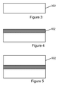
- FIGS. 1 , 2 , and 2 ( a ) are simplified diagrams illustrating a conventional method of forming a stacked memory device.
- FIG. 3-14 are simplified diagrams illustrating a method of forming a memory device according to embodiments of the present invention.
- the present invention is directed to memory device. More particularly, embodiments according to the present invention provide a method and a structure for forming a stacked memory device and interconnect structures for the stacked memory device. But it should be recognized that the present invention can have a much broader range of applicability.
- FIG. 1 is a conventional method of forming interconnects for a memory device. Cross section view and top view are shown. This typically occurs in the periphery, or outside, of the memory array.
- the conventional method includes providing a semiconductor substrate 102 having one or more CMOS devices formed.
- the one or more CMOS device usually includes an interconnect structure 104 to control the memory device.
- a first dielectric material 108 is formed overlying the interconnect structure and a plurality of via openings 110 are formed in a region of the first dielectric material. The openings are filled with a conductor material 112 .
- the conductor material in the via structure is isolated by a first planarization process, for example, a polishing process or an etchback process.
- a first metal material is formed overlying the first dielectric material and the via structure.
- the first metal material is patterned and etched to form the bottom wiring structure 114 for the memory array.
- the conventional method then forms one or more switching region overlying the bottom wiring structure for the memory device and form a second dielectric material overlying the first bottom wiring structure while a surface region of the one or more switching region is exposed.
- FIG. 2 illustrates the steps of forming a top wiring structure according to the conventional method.
- Cross section view and a top view of a peripheral region are shown.
- a second via opening 202 is formed in a portion of the second dielectric material and the first dielectric material stack 204 to expose a surface region of the interconnect of the controlling circuitry.
- a conductor material 206 is formed to fill the second via openings and a second planarizing process is performed to remove the conductor material from the second dielectric material surface and to isolate the top wiring material in the second via structures.
- a top wiring material is formed overlying the second dielectric material and overlying the second via structure. The top wiring material is subjected to a second pattern and etch process to form a top wiring structure 208 .
- the bottom wiring structure and the top wiring structure are spatially arranged perpendicular to each other.
- the switching region is formed in an intersecting region formed from the top wiring structure and the bottom wiring structure in a cell region to form a memory cell.
- the first via structure is formed in a first peripheral area to the memory array and the second via structure is formed in a second peripheral area to the memory array.
- at least three masks are needed to form the first wiring structures and the second wiring structures, and the respective via interconnects.
- the conventional via fabrication method forms a first via connect 220 for a bottom wiring 226 and a second via connect 222 for a top wiring structure 228 for each layer of memory devices.
- the first via connect is disposed in a first periphery region 234 and the second via connect is disposed in a second periphery region 232 , as shown in the top view diagram.
- a switching device 230 is formed between an intersection region of a top wiring structure and a bottom wiring structure in each device layer in the cell region.
- Each of the first via interconnect and the second via interconnect is connected to a respective interconnect of the CMOS devices on the substrate 224 as shown in FIG. 2( a ).
- Each of the layers of memory cells and the respective via structures are formed as in FIGS. 1 and 2 . This includes a total of eight via modules and a costly way to connect each memory layer to the control circuitry on the substrate.
- the present invention provides a method and a structure for forming interconnects for a crossbar array of memory cells and a multilayer (for example one to eight layers) of memory cells.
- a semiconductor substrate 302 is provided.
- the semiconductor substrate can include a single crystal silicon, silicon germanium, or a silicon on insulator (commonly known as SOI) substrate.
- the semiconductor substrate can further include one or more transistor devices formed thereon.
- the one or more transistor devices provide controlling circuitry for the memory device in a specific embodiment.
- a metal, interconnect structure from the controlling circuitry is formed overlying the substrate in a specific embodiment.
- the method includes forming a first dielectric material 502 overlying the substrate including the first metal interconnect structure as shown in FIG. 5 .
- the first dielectric material can be a silicon oxide, a silicon nitride, a silicon oxide on silicon nitride on silicon oxide stack (ONO) depending on the embodiment.
- the first dielectric material can be deposited using a chemical vapor deposition (CVD) process, including plasma enhanced CVD, low pressure CVD, spin on glass (SOG), or any combination of these.
- the silicon oxide material can be doped using boron, phosphorous, fluorine or other material to provide for a suitable and desirable characteristic depending on the application.
- the method subjects the first dielectric material to a first pattern and etch process to form a first via opening 602 in a first peripheral region while a cell region is masked in a specific embodiment.
- a first wiring material 604 is deposited to fill the via and to form a thickness of first wiring material 606 overlying the first dielectric material at least in the cell array region in a specific embodiment.
- a diffusion barrier layer and/or an adhesion layer is usually first deposited conformably overlying the first via opening.
- the adhesion layer can be titanium, titanium nitride, tantalum nitride, tungsten nitride, depending on the application.
- the first wiring material can be copper, aluminum, silver, or tungsten depending on the application.
- the first wiring material used depends on the aspect ratio of via opening 602 .
- aluminum, copper, or silver can be used as that first wiring material in a specific embodiment.
- tungsten may be used.
- the first wiring material may be deposited using techniques such as sputtering, chemical vapor deposition, electrochemical deposition such as electroless deposition or electroplating, including any combination of these, and others.
- sputtering chemical vapor deposition
- electrochemical deposition such as electroless deposition or electroplating
- the method includes depositing a contact material overlying the first wiring material and a resistive switching material and a resistive switching material is formed overlying the contact material.
- the contact material can be a polysilicon material in a specific embodiment.
- the polysilicon material controls a defect density overlying the first wiring material in a specific embodiment.
- the polysilicon material is preferably doped to have a p-type impurity characteristic.
- the polysilicon material is configured to have a suitable conductivity and a suitable contact resistance between the amorphous silicon material and the first wiring material in a specific embodiment.
- the contact material can be optional.
- the method subjects the resistive switching material, the contact material, and the first wiring material to a second pattern and etch process to form a first structure in the cell region.
- the first structure including a first wiring structure 702 in a specific embodiment.
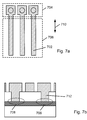
- FIG. 7 a illustrates a top view
- FIG. 7 b illustrates a cross section view.
- the first wiring structure is elongated in shape and configured to extend in a first direction 710 as shown in the top view in FIG. 7 a .
- the first wiring structure includes a bottom electrode structure in cell array 706 region and a via structure 712 in the first peripheral region as show in FIGS. 7 a and 7 b .
- the via structure electrically connects 708 the first wiring structure to respective transistor device formed on the substrate in a specific embodiment.
- the method forms a third dielectric material overlying the first structure and fills a gap region between the first structures.
- the third dielectric material is subjected to a planarization step to expose a resistive switching material surface in a specific embodiment.
- the method includes forming a fourth dielectric material 804 overlying the first structure and include a thickness overlying the resistive switching material.
- the third dielectric material is subjected to a third pattern and etch process to form an opening region in the third dielectric material to expose a portion of the resistive switching material surface in a specific embodiment.
- a suitable conductor material is preferentially formed in the opening region in contact with the resistive switching material.
- the conductor material can be a metal material such as silver, platinum, gold, nickel, aluminum, and others.
- the conductor material used is silver deposited using physical vapor deposition, chemical vapor deposition, electrochemical, including electroplating and electroless plating, and a combination depending on the application.
- the method includes forming a second via opening region in a portion of the third dielectric material, the second dielectric material, and the first dielectric material in a second peripheral region of the cell array while masking the cell region.
- a second wiring material is formed overlying the conductor material and fills the second via opening region.
- the second wiring material can be copper, aluminum, tungsten, or silver depending on the application.
- the second wiring material further fills the second via opening and form a thickness of the second wiring material overlying the conductor material in a specific embodiment.
- the method subjects the second wiring material to a third pattern and etch process to form a second wiring structure 802 .
- the second wiring structure is spatially arranged in a second direction at an angle to the first direction and includes a second via structure disposed in the second peripheral region in a specific embodiment.
- the second wiring structure includes a portion overlying the switching elements in the cell array region in a specific embodiment.
- a top view 806 of the memory device also shown.
- the present invention provides a method and a structure for forming vertical interconnects for a multilayer or stacked memory cell device.
- the multilayer cell device can include one to eight layers of cell array.
- each of the cell array is configured as a crossbar array.
- the method includes providing a substrate having a surface region.
- the substrate includes one or more transistor devices for controlling circuitry for the memory device.
- a first dielectric material is formed overlying the semiconductor substrate.
- the method defines a cell region, a first peripheral region, and a second peripheral region.
- the method forms a first bottom wiring structure overlying the first dielectric material.
- the first bottom wiring structure is spatially extending in a first direction and includes at least a first portion disposed in the first peripheral region.
- the method forms a first switching region overlying the first bottom wiring structure in a specific embodiment.
- a first top wiring structure is formed overlying the first switching region.
- the first top wiring structure is configured to extend in a second direction orthogonal to the first bottom wiring structure forming a first crossbar array of memory cells.
- the first top wiring structure further includes a portion disposed in a second peripheral region and includes a via structure configured in the second peripheral region electrically connected to a respective controlling circuitry in a specific embodiment.
- the switching region is sandwiched in an intersection region between the first top wiring structure and the first bottom wiring structure in the cell array region in a specific embodiment.
- the method includes forming a fourth dielectric material overlying the first top wiring structure of the first crossbar array of memory cells of memory devices.
- the method forms a second bottom wiring structure for the second crossbar array of memory cells overlying the second dielectric material.
- the second bottom wiring structure is configured to extend parallel to the first bottom wiring structure separated by a dielectric stack comprising of each of the dielectric materials in a specific embodiment.
- the method forms a first via opening 902 in a portion of a thickness of dielectric material in a first peripheral region 900 as shown in FIG. 9 .
- Cell region 901 is also shown.
- the first via opening exposes a portion 904 of the first bottom wiring structure and further extends to expose a portion 906 of an interconnect conductor of the transistor device in a specific embodiment.
- the first via opening is formed by a pattern and a dielectric etch process and includes a first opening region 908 and a second opening region 910 , and the first opening region is larger than the second opening region in a specific embodiment.
- the method deposits a second bottom wiring material to fill the first via opening to form a first via structure 1002 .
- the second bottom wiring material further forms a thickness overlying the dielectric material in a specific embodiment.
- the method includes subjecting the second bottom wiring material to a pattern and etch process to form a second bottom wiring structure 1004 in the cell region.
- the first via structure is common to a first bottom wiring structure 1008 and the second bottom wiring structure and connects the second bottom wiring structure and the first bottom wiring stricture to an interconnect 1010 of the transistor on the substrate in a specific embodiment.
- the second bottom wiring structure is configured to extend in a direction parallel to the first bottom wiring structure.
- the present embodiment forms an interconnect structure to provide connection of the first array of memory device and the second array of memory device to the controlling circuitry on the substrate in a single pattern and etch step.
- This is in contrast to the conventional method whereby one via structure is used for each of the memory array thus incur at least two pattern and etch steps for two memory arrays.
- the method forms at least one second switching region overlying the second bottom electrode using the same process as the first switching region in the cell region.
- the method further forms a second top wiring structure overlying the second switching region.
- the second top wiring structure is configured to extend in the second direction and parallel to the first top wiring structure and include a via structure in the second peripheral region 802 in a specific embodiment.
- FIG. 11 illustrates a method and a structure for a via structure to connect multilayer memory device (two or more layers of memory devices) to a respective transistor on the substrate according to an embodiment of the present invention.
- multilayer memory device two or more layers of memory devices
- four layers of memory cells are formed.
- Each of the memory layers may be formed as described for the two memory layer device.
- a first bottom wiring structure 1102 for a first layer of memory device, a second bottom wiring structure 1104 for a second layer of memory device, and a third bottom wiring structure 1106 for a third layer of memory device are illustrated.
- a via opening 1108 is formed in a first peripheral region 1100 .
- the via opening further exposes a portion of the first bottom wiring structure 1110 , a portion of the second bottom wiring structure 1112 , a portion of the third bottom wiring structure 1114 in addition to exposing a portion of an interconnect structure 1116 for the transistor.
- the method deposits a fourth wiring material to fill via opening 1108 to form a via structure 1202 as shown in FIG. 12 .
- the fourth wiring material is usually the same material for each of the first wiring structure, the second wiring structure, and the third wiring structure in a specific embodiment, though different materials may also be used.
- via structure 1202 has a first contact region 1204 with the first bottom wiring structure, a second contact region 1206 with the second bottom wiring structure, and a third contact region 1208 with the third bottom wiring structure in a specific embodiment.
- Via structure 1202 connects the first wiring structure, the second wiring structure, the third wiring structure, and the fourth wiring structure to the substrate 1210 in a specific embodiment.
- the fourth wiring material can be copper, silver, tungsten or aluminum.
- the single via structure can be configured to connect the respective bottom wiring structures of the each of the crossbar memory arrays to the control circuitry on the substrate.
- the single via structure By forming a single via structure to electrically connect, for example, respectively the first bottom wiring structures, the second bottom wiring structure, the third bottom wiring structure and the fourth bottom wiring structure to the controlling circuitry on the substrate, fewer etch steps are needed, greatly simplifies the fabricating process.
- top wiring structures 1302 for each of the respective device layers are configured to connect to their respective controlling circuitry 1304 on the substrate using their respective via structures 1306 or respective signal vias.
- the top wiring via structures are disposed in a second peripheral region in a specific embodiment.
- FIG. 14 illustrates a top view of the four layer memory device structure.
- a single via structure 1402 connects, for example, the respective bottom wiring structures for each of the crossbar layers of memory cell are configured in first peripheral region.
- the respective top wiring structures of each of the respective device layers arrays is connected to the respective control circuits using their respective via structure 1404 , 1406 , 1408 , and 1410 .
- the via structure can be form in more than one steps.
- a first via structure connecting the first bottom wiring structure and the second bottom wiring structure to the controlling circuitry on the substrate is formed.
- a second via structure can be formed in a separate step to connect the third and the fourth bottom wiring structures to the first via structure.
- the first via structure and the second via structure would have a smaller aspect ratio and aluminum can be used as the wiring material in a specific embodiment.
- one skilled in the art would recognize other variations, modifications, and alternatives.
- the present invention has been described using a via structure to connect the bottom wiring structures of a stack of memory cells.
- the top wiring structures may be electrically connected using a single via structure and the bottom wiring structures can each be connected to their respective controlling transistors on the substrate using respective via structures.
- the one via connecting many cells might be called a “mast” via, while the single vias connecting to a single layer are called “signal” vias.
Landscapes
- Engineering & Computer Science (AREA)
- Physics & Mathematics (AREA)
- Condensed Matter Physics & Semiconductors (AREA)
- General Physics & Mathematics (AREA)
- Computer Hardware Design (AREA)
- Microelectronics & Electronic Packaging (AREA)
- Power Engineering (AREA)
- Manufacturing & Machinery (AREA)
- Semiconductor Memories (AREA)
Abstract
Description
Claims (22)
Priority Applications (3)
| Application Number | Priority Date | Filing Date | Title |
|---|---|---|---|
| US12/939,824 US8258020B2 (en) | 2010-11-04 | 2010-11-04 | Interconnects for stacked non-volatile memory device and method |
| US13/532,019 US8399307B2 (en) | 2010-11-04 | 2012-06-25 | Interconnects for stacked non-volatile memory device and method |
| US13/764,698 US9659819B2 (en) | 2010-11-04 | 2013-02-11 | Interconnects for stacked non-volatile memory device and method |
Applications Claiming Priority (1)
| Application Number | Priority Date | Filing Date | Title |
|---|---|---|---|
| US12/939,824 US8258020B2 (en) | 2010-11-04 | 2010-11-04 | Interconnects for stacked non-volatile memory device and method |
Related Child Applications (1)
| Application Number | Title | Priority Date | Filing Date |
|---|---|---|---|
| US13/532,019 Division US8399307B2 (en) | 2010-11-04 | 2012-06-25 | Interconnects for stacked non-volatile memory device and method |
Publications (2)
| Publication Number | Publication Date |
|---|---|
| US20120112155A1 US20120112155A1 (en) | 2012-05-10 |
| US8258020B2 true US8258020B2 (en) | 2012-09-04 |
Family
ID=46018736
Family Applications (3)
| Application Number | Title | Priority Date | Filing Date |
|---|---|---|---|
| US12/939,824 Active 2030-12-09 US8258020B2 (en) | 2010-11-04 | 2010-11-04 | Interconnects for stacked non-volatile memory device and method |
| US13/532,019 Active US8399307B2 (en) | 2010-11-04 | 2012-06-25 | Interconnects for stacked non-volatile memory device and method |
| US13/764,698 Active US9659819B2 (en) | 2010-11-04 | 2013-02-11 | Interconnects for stacked non-volatile memory device and method |
Family Applications After (2)
| Application Number | Title | Priority Date | Filing Date |
|---|---|---|---|
| US13/532,019 Active US8399307B2 (en) | 2010-11-04 | 2012-06-25 | Interconnects for stacked non-volatile memory device and method |
| US13/764,698 Active US9659819B2 (en) | 2010-11-04 | 2013-02-11 | Interconnects for stacked non-volatile memory device and method |
Country Status (1)
| Country | Link |
|---|---|
| US (3) | US8258020B2 (en) |
Cited By (45)
| Publication number | Priority date | Publication date | Assignee | Title |
|---|---|---|---|---|
| US8467227B1 (en) | 2010-11-04 | 2013-06-18 | Crossbar, Inc. | Hetero resistive switching material layer in RRAM device and method |
| US8599601B2 (en) | 2010-06-11 | 2013-12-03 | Crossbar, Inc. | Interface control for improved switching in RRAM |
| US8659929B2 (en) | 2011-06-30 | 2014-02-25 | Crossbar, Inc. | Amorphous silicon RRAM with non-linear device and operation |
| US8716098B1 (en) | 2012-03-09 | 2014-05-06 | Crossbar, Inc. | Selective removal method and structure of silver in resistive switching device for a non-volatile memory device |
| US8750019B2 (en) | 2010-07-09 | 2014-06-10 | Crossbar, Inc. | Resistive memory using SiGe material |
| US8791010B1 (en) | 2010-12-31 | 2014-07-29 | Crossbar, Inc. | Silver interconnects for stacked non-volatile memory device and method |
| US8796658B1 (en) | 2012-05-07 | 2014-08-05 | Crossbar, Inc. | Filamentary based non-volatile resistive memory device and method |
| US8809831B2 (en) | 2010-07-13 | 2014-08-19 | Crossbar, Inc. | On/off ratio for non-volatile memory device and method |
| US8884261B2 (en) | 2010-08-23 | 2014-11-11 | Crossbar, Inc. | Device switching using layered device structure |
| US8912523B2 (en) | 2010-09-29 | 2014-12-16 | Crossbar, Inc. | Conductive path in switching material in a resistive random access memory device and control |
| US8934280B1 (en) | 2013-02-06 | 2015-01-13 | Crossbar, Inc. | Capacitive discharge programming for two-terminal memory cells |
| US8946046B1 (en) | 2012-05-02 | 2015-02-03 | Crossbar, Inc. | Guided path for forming a conductive filament in RRAM |
| US8947908B2 (en) | 2010-11-04 | 2015-02-03 | Crossbar, Inc. | Hetero-switching layer in a RRAM device and method |
| US8993397B2 (en) | 2010-06-11 | 2015-03-31 | Crossbar, Inc. | Pillar structure for memory device and method |
| US9012307B2 (en) | 2010-07-13 | 2015-04-21 | Crossbar, Inc. | Two terminal resistive switching device structure and method of fabricating |
| US9035276B2 (en) | 2010-08-23 | 2015-05-19 | Crossbar, Inc. | Stackable non-volatile resistive switching memory device |
| US9087576B1 (en) | 2012-03-29 | 2015-07-21 | Crossbar, Inc. | Low temperature fabrication method for a three-dimensional memory device and structure |
| US9112145B1 (en) | 2013-01-31 | 2015-08-18 | Crossbar, Inc. | Rectified switching of two-terminal memory via real time filament formation |
| US9129887B2 (en) | 2010-09-29 | 2015-09-08 | Crossbar, Inc. | Resistor structure for a non-volatile memory device and method |
| US9153623B1 (en) | 2010-12-31 | 2015-10-06 | Crossbar, Inc. | Thin film transistor steering element for a non-volatile memory device |
| US9191000B2 (en) | 2011-07-29 | 2015-11-17 | Crossbar, Inc. | Field programmable gate array utilizing two-terminal non-volatile memory |
| US9312483B2 (en) | 2012-09-24 | 2016-04-12 | Crossbar, Inc. | Electrode structure for a non-volatile memory device and method |
| US9324942B1 (en) | 2013-01-31 | 2016-04-26 | Crossbar, Inc. | Resistive memory cell with solid state diode |
| US9401475B1 (en) | 2010-08-23 | 2016-07-26 | Crossbar, Inc. | Method for silver deposition for a non-volatile memory device |
| US9406379B2 (en) | 2013-01-03 | 2016-08-02 | Crossbar, Inc. | Resistive random access memory with non-linear current-voltage relationship |
| US9543359B2 (en) | 2011-05-31 | 2017-01-10 | Crossbar, Inc. | Switching device having a non-linear element |
| US9564587B1 (en) | 2011-06-30 | 2017-02-07 | Crossbar, Inc. | Three-dimensional two-terminal memory with enhanced electric field and segmented interconnects |
| US9570678B1 (en) | 2010-06-08 | 2017-02-14 | Crossbar, Inc. | Resistive RAM with preferental filament formation region and methods |
| US9576616B2 (en) | 2012-10-10 | 2017-02-21 | Crossbar, Inc. | Non-volatile memory with overwrite capability and low write amplification |
| US9583701B1 (en) | 2012-08-14 | 2017-02-28 | Crossbar, Inc. | Methods for fabricating resistive memory device switching material using ion implantation |
| USRE46335E1 (en) | 2010-11-04 | 2017-03-07 | Crossbar, Inc. | Switching device having a non-linear element |
| US9601690B1 (en) | 2011-06-30 | 2017-03-21 | Crossbar, Inc. | Sub-oxide interface layer for two-terminal memory |
| US9601692B1 (en) | 2010-07-13 | 2017-03-21 | Crossbar, Inc. | Hetero-switching layer in a RRAM device and method |
| US9620206B2 (en) | 2011-05-31 | 2017-04-11 | Crossbar, Inc. | Memory array architecture with two-terminal memory cells |
| US9627443B2 (en) | 2011-06-30 | 2017-04-18 | Crossbar, Inc. | Three-dimensional oblique two-terminal memory with enhanced electric field |
| US9633723B2 (en) | 2011-06-23 | 2017-04-25 | Crossbar, Inc. | High operating speed resistive random access memory |
| US9673255B2 (en) | 2012-04-05 | 2017-06-06 | Crossbar, Inc. | Resistive memory device and fabrication methods |
| US9685608B2 (en) | 2012-04-13 | 2017-06-20 | Crossbar, Inc. | Reduced diffusion in metal electrode for two-terminal memory |
| US9729155B2 (en) | 2011-07-29 | 2017-08-08 | Crossbar, Inc. | Field programmable gate array utilizing two-terminal non-volatile memory |
| US9735358B2 (en) | 2012-08-14 | 2017-08-15 | Crossbar, Inc. | Noble metal / non-noble metal electrode for RRAM applications |
| US9741765B1 (en) | 2012-08-14 | 2017-08-22 | Crossbar, Inc. | Monolithically integrated resistive memory using integrated-circuit foundry compatible processes |
| US9793474B2 (en) | 2012-04-20 | 2017-10-17 | Crossbar, Inc. | Low temperature P+ polycrystalline silicon material for non-volatile memory device |
| US10056907B1 (en) | 2011-07-29 | 2018-08-21 | Crossbar, Inc. | Field programmable gate array utilizing two-terminal non-volatile memory |
| US10290801B2 (en) | 2014-02-07 | 2019-05-14 | Crossbar, Inc. | Scalable silicon based resistive memory device |
| US11068620B2 (en) | 2012-11-09 | 2021-07-20 | Crossbar, Inc. | Secure circuit integrated with memory layer |
Families Citing this family (9)
| Publication number | Priority date | Publication date | Assignee | Title |
|---|---|---|---|---|
| US8841196B1 (en) | 2010-09-29 | 2014-09-23 | Crossbar, Inc. | Selective deposition of silver for non-volatile memory device fabrication |
| US8187945B2 (en) | 2010-10-27 | 2012-05-29 | Crossbar, Inc. | Method for obtaining smooth, continuous silver film |
| US8258020B2 (en) * | 2010-11-04 | 2012-09-04 | Crossbar Inc. | Interconnects for stacked non-volatile memory device and method |
| US8946667B1 (en) | 2012-04-13 | 2015-02-03 | Crossbar, Inc. | Barrier structure for a silver based RRAM and method |
| US8765566B2 (en) | 2012-05-10 | 2014-07-01 | Crossbar, Inc. | Line and space architecture for a non-volatile memory device |
| US9070859B1 (en) | 2012-05-25 | 2015-06-30 | Crossbar, Inc. | Low temperature deposition method for polycrystalline silicon material for a non-volatile memory device |
| US8883603B1 (en) | 2012-08-01 | 2014-11-11 | Crossbar, Inc. | Silver deposition method for a non-volatile memory device |
| US8796102B1 (en) | 2012-08-29 | 2014-08-05 | Crossbar, Inc. | Device structure for a RRAM and method |
| KR102163708B1 (en) * | 2014-04-18 | 2020-10-12 | 에스케이하이닉스 주식회사 | Semiconductor package and the method for fabricating of the same |
Citations (32)
| Publication number | Priority date | Publication date | Assignee | Title |
|---|---|---|---|---|
| US20040194340A1 (en) | 1998-10-14 | 2004-10-07 | Tokyo Electron Limited | Method and apparatus for surface treatment |
| US6939787B2 (en) | 1999-12-28 | 2005-09-06 | Fujitsu Limited | Method for fabricating semiconductor device having gate electrode with polymetal structure of polycrystalline silicon film and metal film |
| US7023093B2 (en) * | 2002-10-24 | 2006-04-04 | International Business Machines Corporation | Very low effective dielectric constant interconnect Structures and methods for fabricating the same |
| US20070087508A1 (en) | 2003-12-03 | 2007-04-19 | Herner S B | Method for making a p-i-n diode crystallized adjacent to a silicide in series with a dielectric antifuse |
| US20070105390A1 (en) | 2005-11-09 | 2007-05-10 | Oh Travis B | Oxygen depleted etching process |
| US7238607B2 (en) | 2002-12-19 | 2007-07-03 | Sandisk 3D Llc | Method to minimize formation of recess at surface planarized by chemical mechanical planarization |
| US7474000B2 (en) | 2003-12-05 | 2009-01-06 | Sandisk 3D Llc | High density contact to relaxed geometry layers |
| US7550380B2 (en) | 2004-11-03 | 2009-06-23 | Micron Technology, Inc. | Electroless plating of metal caps for chalcogenide-based memory devices |
| US20090256130A1 (en) | 2008-04-11 | 2009-10-15 | Sandisk 3D Llc | Memory cell that employs a selectively fabricated carbon nano-tube reversible resistance-switching element, and methods of forming the same |
| US20100012914A1 (en) | 2008-07-18 | 2010-01-21 | Sandisk 3D Llc | Carbon-based resistivity-switching materials and methods of forming the same |
| US20100019310A1 (en) | 2008-07-25 | 2010-01-28 | Kabushiki Kaisha Toshiba | Semiconductor memory device |
| US20100085798A1 (en) | 2008-10-08 | 2010-04-08 | The Regents Of The University Of Michigan | Silicon-based nanoscale resistive device with adjustable resistance |
| US20100084625A1 (en) | 2008-10-02 | 2010-04-08 | Guy Wicker | Memory Device |
| US20100090192A1 (en) | 2006-08-31 | 2010-04-15 | Nxp, B.V. | Method for controlled formation of the resistive switching material in a resistive switching device and device obtained thereof |
| US20100101290A1 (en) | 2008-10-24 | 2010-04-29 | Antonio Bertolotto | Method for the production of an agent for treatment of agricultural soils |
| US20100102290A1 (en) | 2008-10-20 | 2010-04-29 | The Regents Of The University Of Michigan | Silicon based nanoscale crossbar memory |
| US20100157710A1 (en) | 2008-12-19 | 2010-06-24 | Unity Semiconductor Corporation | Array Operation Using A Schottky Diode As a Non-Ohmic Isolation Device |
| US7786589B2 (en) * | 2006-12-06 | 2010-08-31 | Kabushiki Kaisha Toshiba | Semiconductor device and method for manufacturing semiconductor device |
| US7824956B2 (en) | 2007-06-29 | 2010-11-02 | Sandisk 3D Llc | Memory cell that employs a selectively grown reversible resistance-switching element and methods of forming the same |
| US7829875B2 (en) | 2006-03-31 | 2010-11-09 | Sandisk 3D Llc | Nonvolatile rewritable memory cell comprising a resistivity-switching oxide or nitride and an antifuse |
| KR20110014248A (en) | 2010-11-28 | 2011-02-10 | 오세영 | A driver to set up lighting slab at night throngh solar panel |
| US20110133149A1 (en) | 2009-12-04 | 2011-06-09 | Sonehara Takeshi | Resistance change memory and manufacturing method thereof |
| US7968419B2 (en) | 2005-07-18 | 2011-06-28 | Sharp Laboratories Of America, Inc. | Back-to-back metal/semiconductor/metal (MSM) Schottky diode |
| US20110284814A1 (en) | 2010-05-24 | 2011-11-24 | Guobiao Zhang | Large Bit-Per-Cell Three-Dimensional Mask-Programmable Read-Only Memory |
| US8088688B1 (en) | 2010-11-05 | 2012-01-03 | Crossbar, Inc. | p+ polysilicon material on aluminum for non-volatile memory device and method |
| US20120008366A1 (en) | 2010-07-09 | 2012-01-12 | Crossbar, Inc. | RESTIVE MEMORY USING SiGe MATERIAL |
| US8097874B2 (en) | 2008-10-30 | 2012-01-17 | Seagate Technology Llc | Programmable resistive memory cell with sacrificial metal |
| US20120012806A1 (en) | 2010-07-13 | 2012-01-19 | Crossbar, Inc. | Improved on/off ratio for non-volatile memory device and method |
| US20120015506A1 (en) | 2010-07-13 | 2012-01-19 | Crossbar, Inc. | Two terminal resistive switching device structure and method of fabricating |
| US20120025161A1 (en) | 2008-02-27 | 2012-02-02 | Manuj Rathor | Diode and resistive memory device structures |
| US20120033479A1 (en) | 2010-08-06 | 2012-02-09 | Lsi Corporation | Modification of logic by morphological manipulation of a semiconductor resistive element |
| US20120043654A1 (en) | 2010-08-19 | 2012-02-23 | Taiwan Semiconductor Manufacturing Company, Ltd. | Mechanisms for forming copper pillar bumps using patterned anodes |
Family Cites Families (24)
| Publication number | Priority date | Publication date | Assignee | Title |
|---|---|---|---|---|
| JPH0590224A (en) | 1991-01-22 | 1993-04-09 | Toshiba Corp | Manufacture of semiconductor device |
| US7109056B2 (en) | 2001-09-20 | 2006-09-19 | Micron Technology, Inc. | Electro-and electroless plating of metal in the manufacture of PCRAM devices |
| US7087919B2 (en) | 2002-02-20 | 2006-08-08 | Micron Technology, Inc. | Layered resistance variable memory device and method of fabrication |
| US7176064B2 (en) | 2003-12-03 | 2007-02-13 | Sandisk 3D Llc | Memory cell comprising a semiconductor junction diode crystallized adjacent to a silicide |
| US7005350B2 (en) * | 2002-12-31 | 2006-02-28 | Matrix Semiconductor, Inc. | Method for fabricating programmable memory array structures incorporating series-connected transistor strings |
| US7405465B2 (en) | 2004-09-29 | 2008-07-29 | Sandisk 3D Llc | Deposited semiconductor structure to minimize n-type dopant diffusion and method of making |
| US7426128B2 (en) | 2005-07-11 | 2008-09-16 | Sandisk 3D Llc | Switchable resistive memory with opposite polarity write pulses |
| US7972897B2 (en) * | 2007-02-05 | 2011-07-05 | Intermolecular, Inc. | Methods for forming resistive switching memory elements |
| JP5175526B2 (en) * | 2007-11-22 | 2013-04-03 | 株式会社東芝 | Nonvolatile semiconductor memory device and manufacturing method thereof |
| US8557685B2 (en) | 2008-08-07 | 2013-10-15 | Sandisk 3D Llc | Memory cell that includes a carbon-based memory element and methods of forming the same |
| JP5288933B2 (en) * | 2008-08-08 | 2013-09-11 | 株式会社東芝 | Semiconductor memory device and manufacturing method thereof |
| US7858468B2 (en) | 2008-10-30 | 2010-12-28 | Micron Technology, Inc. | Memory devices and formation methods |
| US8623697B2 (en) | 2008-12-31 | 2014-01-07 | Micron Technology, Inc. | Avoiding degradation of chalcogenide material during definition of multilayer stack structure |
| KR101033468B1 (en) * | 2009-06-30 | 2011-05-09 | 주식회사 하이닉스반도체 | Phase Change Memory Device Being Able to Improve Resistance of Word Line, Layout Structure of The Same, and Method of Manufacturing The Same |
| JP4945619B2 (en) * | 2009-09-24 | 2012-06-06 | 株式会社東芝 | Semiconductor memory device |
| US8198144B2 (en) | 2010-06-11 | 2012-06-12 | Crossbar, Inc. | Pillar structure for memory device and method |
| US8351241B2 (en) * | 2010-06-24 | 2013-01-08 | The Regents Of The University Of Michigan | Rectification element and method for resistive switching for non volatile memory device |
| US8492195B2 (en) | 2010-08-23 | 2013-07-23 | Crossbar, Inc. | Method for forming stackable non-volatile resistive switching memory devices |
| US8558212B2 (en) | 2010-09-29 | 2013-10-15 | Crossbar, Inc. | Conductive path in switching material in a resistive random access memory device and control |
| US8723154B2 (en) | 2010-09-29 | 2014-05-13 | Crossbar, Inc. | Integration of an amorphous silicon resistive switching device |
| US8389971B2 (en) | 2010-10-14 | 2013-03-05 | Sandisk 3D Llc | Memory cells having storage elements that share material layers with steering elements and methods of forming the same |
| US8187945B2 (en) | 2010-10-27 | 2012-05-29 | Crossbar, Inc. | Method for obtaining smooth, continuous silver film |
| US8258020B2 (en) * | 2010-11-04 | 2012-09-04 | Crossbar Inc. | Interconnects for stacked non-volatile memory device and method |
| JP5812330B2 (en) | 2011-03-31 | 2015-11-11 | 日本電産株式会社 | Motor and disk drive device |
-
2010
- 2010-11-04 US US12/939,824 patent/US8258020B2/en active Active
-
2012
- 2012-06-25 US US13/532,019 patent/US8399307B2/en active Active
-
2013
- 2013-02-11 US US13/764,698 patent/US9659819B2/en active Active
Patent Citations (32)
| Publication number | Priority date | Publication date | Assignee | Title |
|---|---|---|---|---|
| US20040194340A1 (en) | 1998-10-14 | 2004-10-07 | Tokyo Electron Limited | Method and apparatus for surface treatment |
| US6939787B2 (en) | 1999-12-28 | 2005-09-06 | Fujitsu Limited | Method for fabricating semiconductor device having gate electrode with polymetal structure of polycrystalline silicon film and metal film |
| US7023093B2 (en) * | 2002-10-24 | 2006-04-04 | International Business Machines Corporation | Very low effective dielectric constant interconnect Structures and methods for fabricating the same |
| US7238607B2 (en) | 2002-12-19 | 2007-07-03 | Sandisk 3D Llc | Method to minimize formation of recess at surface planarized by chemical mechanical planarization |
| US20070087508A1 (en) | 2003-12-03 | 2007-04-19 | Herner S B | Method for making a p-i-n diode crystallized adjacent to a silicide in series with a dielectric antifuse |
| US7474000B2 (en) | 2003-12-05 | 2009-01-06 | Sandisk 3D Llc | High density contact to relaxed geometry layers |
| US7550380B2 (en) | 2004-11-03 | 2009-06-23 | Micron Technology, Inc. | Electroless plating of metal caps for chalcogenide-based memory devices |
| US7968419B2 (en) | 2005-07-18 | 2011-06-28 | Sharp Laboratories Of America, Inc. | Back-to-back metal/semiconductor/metal (MSM) Schottky diode |
| US20070105390A1 (en) | 2005-11-09 | 2007-05-10 | Oh Travis B | Oxygen depleted etching process |
| US7829875B2 (en) | 2006-03-31 | 2010-11-09 | Sandisk 3D Llc | Nonvolatile rewritable memory cell comprising a resistivity-switching oxide or nitride and an antifuse |
| US20100090192A1 (en) | 2006-08-31 | 2010-04-15 | Nxp, B.V. | Method for controlled formation of the resistive switching material in a resistive switching device and device obtained thereof |
| US7786589B2 (en) * | 2006-12-06 | 2010-08-31 | Kabushiki Kaisha Toshiba | Semiconductor device and method for manufacturing semiconductor device |
| US7824956B2 (en) | 2007-06-29 | 2010-11-02 | Sandisk 3D Llc | Memory cell that employs a selectively grown reversible resistance-switching element and methods of forming the same |
| US20120025161A1 (en) | 2008-02-27 | 2012-02-02 | Manuj Rathor | Diode and resistive memory device structures |
| US20090256130A1 (en) | 2008-04-11 | 2009-10-15 | Sandisk 3D Llc | Memory cell that employs a selectively fabricated carbon nano-tube reversible resistance-switching element, and methods of forming the same |
| US20100012914A1 (en) | 2008-07-18 | 2010-01-21 | Sandisk 3D Llc | Carbon-based resistivity-switching materials and methods of forming the same |
| US20100019310A1 (en) | 2008-07-25 | 2010-01-28 | Kabushiki Kaisha Toshiba | Semiconductor memory device |
| US20100084625A1 (en) | 2008-10-02 | 2010-04-08 | Guy Wicker | Memory Device |
| US20100085798A1 (en) | 2008-10-08 | 2010-04-08 | The Regents Of The University Of Michigan | Silicon-based nanoscale resistive device with adjustable resistance |
| US20100102290A1 (en) | 2008-10-20 | 2010-04-29 | The Regents Of The University Of Michigan | Silicon based nanoscale crossbar memory |
| US20100101290A1 (en) | 2008-10-24 | 2010-04-29 | Antonio Bertolotto | Method for the production of an agent for treatment of agricultural soils |
| US8097874B2 (en) | 2008-10-30 | 2012-01-17 | Seagate Technology Llc | Programmable resistive memory cell with sacrificial metal |
| US20100157710A1 (en) | 2008-12-19 | 2010-06-24 | Unity Semiconductor Corporation | Array Operation Using A Schottky Diode As a Non-Ohmic Isolation Device |
| US20110133149A1 (en) | 2009-12-04 | 2011-06-09 | Sonehara Takeshi | Resistance change memory and manufacturing method thereof |
| US20110284814A1 (en) | 2010-05-24 | 2011-11-24 | Guobiao Zhang | Large Bit-Per-Cell Three-Dimensional Mask-Programmable Read-Only Memory |
| US20120008366A1 (en) | 2010-07-09 | 2012-01-12 | Crossbar, Inc. | RESTIVE MEMORY USING SiGe MATERIAL |
| US20120012806A1 (en) | 2010-07-13 | 2012-01-19 | Crossbar, Inc. | Improved on/off ratio for non-volatile memory device and method |
| US20120015506A1 (en) | 2010-07-13 | 2012-01-19 | Crossbar, Inc. | Two terminal resistive switching device structure and method of fabricating |
| US20120033479A1 (en) | 2010-08-06 | 2012-02-09 | Lsi Corporation | Modification of logic by morphological manipulation of a semiconductor resistive element |
| US20120043654A1 (en) | 2010-08-19 | 2012-02-23 | Taiwan Semiconductor Manufacturing Company, Ltd. | Mechanisms for forming copper pillar bumps using patterned anodes |
| US8088688B1 (en) | 2010-11-05 | 2012-01-03 | Crossbar, Inc. | p+ polysilicon material on aluminum for non-volatile memory device and method |
| KR20110014248A (en) | 2010-11-28 | 2011-02-10 | 오세영 | A driver to set up lighting slab at night throngh solar panel |
Non-Patent Citations (18)
| Title |
|---|
| European Search Report for Application No. EP 1100 5207.3 of Oct. 12, 2011. |
| Hao-Chih Yuan et al, "Silicon Solar Cells with Front Hetero-Contact and Aluminum Alloy Back Junction", NREL Conference Paper CP-520-42566, 33rd IEEE Photovoltaic Specialists Conference, May 11-16, 2008, National Renewable Energy Laboratory, San Diego, California. |
| International Search Report for PCT/US2011/045124 filed on Jul. 22, 2011. |
| J. Del Alamo et al, "Operating limits of Al-alloyed high-low junction for BSF solar cells", Solid-State Electronics, 1981, pp. 415-420, vol. 24, Pergamon Press Ltd., Great Britain. |
| Notice of Allowance for U.S. Appl. No. 12/833,898 dated May 30, 2012. |
| Notice of Allowance for U.S. Appl. No. 12/835,699 dated Feb. 6, 2012. |
| Notice of Allowance for U.S. Appl. No. 12/913,719 dated Mar. 12, 2012. |
| Notice of Allowance for U.S. Appl. No. 12/940,920 dated Oct. 5, 2011. |
| Office Action for U.S. Appl. No. 12/814,410 dated Apr. 17, 2012. |
| Office Action for U.S. Appl. No. 12/833,898 dated Apr. 5, 2012. |
| Office Action for U.S. Appl. No. 12/835,699 dated Aug. 24, 2011. |
| Office Action for U.S. Appl. No. 12/913,719 dated Feb. 17, 2011. |
| Office Action for U.S. Appl. No. 12/913,719 dated Jul. 22, 2011. |
| Office Action for U.S. Appl. No. 13/149,653 dated Apr. 25, 2012. |
| Office Action for U.S. Appl. No. 13/314,513 dated Mar. 27, 2012. |
| Peng-Heng Chang et al, "Aluminum spiking at contact windows in Al/Ti-W/Si", Appl. Phys. Lett. Jan. 25, 1988, pp. 272-274, vol. 52 No. 4, American Institute of Physics. |
| Shong Yin, "Solution Processed Silver Sulfide Thin Films for Filament Memory Applications", Technical Report No. UCB/EECS-2010-166, http://www.eecs.berkeley.edu/Pubs/TechRpts/2010/EECS-2010-166.html, Dec. 17, 2010, Electrical Engineering and Computer Sciences, University of California at Berkeley.. |
| Written Opinion of the International Searching Authority for PCT/US2011/045124 filed on Jul. 22, 2011. |
Cited By (57)
| Publication number | Priority date | Publication date | Assignee | Title |
|---|---|---|---|---|
| US9570678B1 (en) | 2010-06-08 | 2017-02-14 | Crossbar, Inc. | Resistive RAM with preferental filament formation region and methods |
| US8599601B2 (en) | 2010-06-11 | 2013-12-03 | Crossbar, Inc. | Interface control for improved switching in RRAM |
| US8993397B2 (en) | 2010-06-11 | 2015-03-31 | Crossbar, Inc. | Pillar structure for memory device and method |
| US8750019B2 (en) | 2010-07-09 | 2014-06-10 | Crossbar, Inc. | Resistive memory using SiGe material |
| US9036400B2 (en) | 2010-07-09 | 2015-05-19 | Crossbar, Inc. | Method and structure of monolithically integrated IC and resistive memory using IC foundry-compatible processes |
| US9012307B2 (en) | 2010-07-13 | 2015-04-21 | Crossbar, Inc. | Two terminal resistive switching device structure and method of fabricating |
| US9601692B1 (en) | 2010-07-13 | 2017-03-21 | Crossbar, Inc. | Hetero-switching layer in a RRAM device and method |
| US8809831B2 (en) | 2010-07-13 | 2014-08-19 | Crossbar, Inc. | On/off ratio for non-volatile memory device and method |
| US9755143B2 (en) | 2010-07-13 | 2017-09-05 | Crossbar, Inc. | On/off ratio for nonvolatile memory device and method |
| US9401475B1 (en) | 2010-08-23 | 2016-07-26 | Crossbar, Inc. | Method for silver deposition for a non-volatile memory device |
| US8884261B2 (en) | 2010-08-23 | 2014-11-11 | Crossbar, Inc. | Device switching using layered device structure |
| US9412789B1 (en) | 2010-08-23 | 2016-08-09 | Crossbar, Inc. | Stackable non-volatile resistive switching memory device and method of fabricating the same |
| US10224370B2 (en) | 2010-08-23 | 2019-03-05 | Crossbar, Inc. | Device switching using layered device structure |
| US9590013B2 (en) | 2010-08-23 | 2017-03-07 | Crossbar, Inc. | Device switching using layered device structure |
| US9035276B2 (en) | 2010-08-23 | 2015-05-19 | Crossbar, Inc. | Stackable non-volatile resistive switching memory device |
| US8912523B2 (en) | 2010-09-29 | 2014-12-16 | Crossbar, Inc. | Conductive path in switching material in a resistive random access memory device and control |
| US9129887B2 (en) | 2010-09-29 | 2015-09-08 | Crossbar, Inc. | Resistor structure for a non-volatile memory device and method |
| US8947908B2 (en) | 2010-11-04 | 2015-02-03 | Crossbar, Inc. | Hetero-switching layer in a RRAM device and method |
| USRE46335E1 (en) | 2010-11-04 | 2017-03-07 | Crossbar, Inc. | Switching device having a non-linear element |
| US8659933B2 (en) | 2010-11-04 | 2014-02-25 | Crossbar, Inc. | Hereto resistive switching material layer in RRAM device and method |
| US8467227B1 (en) | 2010-11-04 | 2013-06-18 | Crossbar, Inc. | Hetero resistive switching material layer in RRAM device and method |
| US9153623B1 (en) | 2010-12-31 | 2015-10-06 | Crossbar, Inc. | Thin film transistor steering element for a non-volatile memory device |
| US8791010B1 (en) | 2010-12-31 | 2014-07-29 | Crossbar, Inc. | Silver interconnects for stacked non-volatile memory device and method |
| US9543359B2 (en) | 2011-05-31 | 2017-01-10 | Crossbar, Inc. | Switching device having a non-linear element |
| US9620206B2 (en) | 2011-05-31 | 2017-04-11 | Crossbar, Inc. | Memory array architecture with two-terminal memory cells |
| US9633723B2 (en) | 2011-06-23 | 2017-04-25 | Crossbar, Inc. | High operating speed resistive random access memory |
| US9601690B1 (en) | 2011-06-30 | 2017-03-21 | Crossbar, Inc. | Sub-oxide interface layer for two-terminal memory |
| US8659929B2 (en) | 2011-06-30 | 2014-02-25 | Crossbar, Inc. | Amorphous silicon RRAM with non-linear device and operation |
| US9564587B1 (en) | 2011-06-30 | 2017-02-07 | Crossbar, Inc. | Three-dimensional two-terminal memory with enhanced electric field and segmented interconnects |
| US9570683B1 (en) | 2011-06-30 | 2017-02-14 | Crossbar, Inc. | Three-dimensional two-terminal memory with enhanced electric field and segmented interconnects |
| US9627443B2 (en) | 2011-06-30 | 2017-04-18 | Crossbar, Inc. | Three-dimensional oblique two-terminal memory with enhanced electric field |
| US10056907B1 (en) | 2011-07-29 | 2018-08-21 | Crossbar, Inc. | Field programmable gate array utilizing two-terminal non-volatile memory |
| US9191000B2 (en) | 2011-07-29 | 2015-11-17 | Crossbar, Inc. | Field programmable gate array utilizing two-terminal non-volatile memory |
| US9729155B2 (en) | 2011-07-29 | 2017-08-08 | Crossbar, Inc. | Field programmable gate array utilizing two-terminal non-volatile memory |
| US8716098B1 (en) | 2012-03-09 | 2014-05-06 | Crossbar, Inc. | Selective removal method and structure of silver in resistive switching device for a non-volatile memory device |
| US9087576B1 (en) | 2012-03-29 | 2015-07-21 | Crossbar, Inc. | Low temperature fabrication method for a three-dimensional memory device and structure |
| US9673255B2 (en) | 2012-04-05 | 2017-06-06 | Crossbar, Inc. | Resistive memory device and fabrication methods |
| US10910561B1 (en) | 2012-04-13 | 2021-02-02 | Crossbar, Inc. | Reduced diffusion in metal electrode for two-terminal memory |
| US9685608B2 (en) | 2012-04-13 | 2017-06-20 | Crossbar, Inc. | Reduced diffusion in metal electrode for two-terminal memory |
| US9793474B2 (en) | 2012-04-20 | 2017-10-17 | Crossbar, Inc. | Low temperature P+ polycrystalline silicon material for non-volatile memory device |
| US8946046B1 (en) | 2012-05-02 | 2015-02-03 | Crossbar, Inc. | Guided path for forming a conductive filament in RRAM |
| US9972778B2 (en) | 2012-05-02 | 2018-05-15 | Crossbar, Inc. | Guided path for forming a conductive filament in RRAM |
| US8796658B1 (en) | 2012-05-07 | 2014-08-05 | Crossbar, Inc. | Filamentary based non-volatile resistive memory device and method |
| US9385319B1 (en) | 2012-05-07 | 2016-07-05 | Crossbar, Inc. | Filamentary based non-volatile resistive memory device and method |
| US10096653B2 (en) | 2012-08-14 | 2018-10-09 | Crossbar, Inc. | Monolithically integrated resistive memory using integrated-circuit foundry compatible processes |
| US9735358B2 (en) | 2012-08-14 | 2017-08-15 | Crossbar, Inc. | Noble metal / non-noble metal electrode for RRAM applications |
| US9741765B1 (en) | 2012-08-14 | 2017-08-22 | Crossbar, Inc. | Monolithically integrated resistive memory using integrated-circuit foundry compatible processes |
| US9583701B1 (en) | 2012-08-14 | 2017-02-28 | Crossbar, Inc. | Methods for fabricating resistive memory device switching material using ion implantation |
| US9312483B2 (en) | 2012-09-24 | 2016-04-12 | Crossbar, Inc. | Electrode structure for a non-volatile memory device and method |
| US9576616B2 (en) | 2012-10-10 | 2017-02-21 | Crossbar, Inc. | Non-volatile memory with overwrite capability and low write amplification |
| US11068620B2 (en) | 2012-11-09 | 2021-07-20 | Crossbar, Inc. | Secure circuit integrated with memory layer |
| US11836277B2 (en) | 2012-11-09 | 2023-12-05 | Crossbar, Inc. | Secure circuit integrated with memory layer |
| US9406379B2 (en) | 2013-01-03 | 2016-08-02 | Crossbar, Inc. | Resistive random access memory with non-linear current-voltage relationship |
| US9112145B1 (en) | 2013-01-31 | 2015-08-18 | Crossbar, Inc. | Rectified switching of two-terminal memory via real time filament formation |
| US9324942B1 (en) | 2013-01-31 | 2016-04-26 | Crossbar, Inc. | Resistive memory cell with solid state diode |
| US8934280B1 (en) | 2013-02-06 | 2015-01-13 | Crossbar, Inc. | Capacitive discharge programming for two-terminal memory cells |
| US10290801B2 (en) | 2014-02-07 | 2019-05-14 | Crossbar, Inc. | Scalable silicon based resistive memory device |
Also Published As
| Publication number | Publication date |
|---|---|
| US20120273748A1 (en) | 2012-11-01 |
| US20130157457A1 (en) | 2013-06-20 |
| US9659819B2 (en) | 2017-05-23 |
| US20120112155A1 (en) | 2012-05-10 |
| US8399307B2 (en) | 2013-03-19 |
Similar Documents
| Publication | Publication Date | Title |
|---|---|---|
| US8258020B2 (en) | Interconnects for stacked non-volatile memory device and method | |
| US9412789B1 (en) | Stackable non-volatile resistive switching memory device and method of fabricating the same | |
| US8659003B2 (en) | Disturb-resistant non-volatile memory device and method | |
| US9449924B2 (en) | Multilevel contact to a 3D memory array and method of making thereof | |
| US8183552B2 (en) | Semiconductor memory device | |
| US9012307B2 (en) | Two terminal resistive switching device structure and method of fabricating | |
| US9331088B2 (en) | Transistor device with gate bottom isolation and method of making thereof | |
| US20130094273A1 (en) | 3d memory and decoding technologies | |
| US20100038619A1 (en) | Variable resistance element, manufacturing method thereof, and electronic device | |
| US7838921B2 (en) | Memory cell arrangements | |
| US20230380310A1 (en) | Semiconductor memory devices with electrically isolated stacked bit lines and methods of manufacture | |
| US20140319450A1 (en) | Disturb-resistant non-volatile memory device using via-fill and etchback technique | |
| CN113540151A (en) | Memory device and method of forming a memory device | |
| CN113488483A (en) | Three-dimensional memory device and method of manufacturing the same | |
| US8791010B1 (en) | Silver interconnects for stacked non-volatile memory device and method | |
| KR102535546B1 (en) | Dual-layer channel transistor and methods of forming same | |
| US20120309188A1 (en) | Method to improve adhesion for a silver filled oxide via for a non-volatile memory device | |
| CN116963507A (en) | Resistive random access memory and preparation method thereof | |
| TW202137489A (en) | Integrated chip and method for forming the same |
Legal Events
| Date | Code | Title | Description |
|---|---|---|---|
| AS | Assignment |
Owner name: CROSSBAR, INC., CALIFORNIA Free format text: ASSIGNMENT OF ASSIGNORS INTEREST;ASSIGNOR:HERNER, SCOTT BRAD;REEL/FRAME:025328/0137 Effective date: 20101103 |
|
| STCF | Information on status: patent grant |
Free format text: PATENTED CASE |
|
| FEPP | Fee payment procedure |
Free format text: PAYER NUMBER DE-ASSIGNED (ORIGINAL EVENT CODE: RMPN); ENTITY STATUS OF PATENT OWNER: LARGE ENTITY Free format text: PAYOR NUMBER ASSIGNED (ORIGINAL EVENT CODE: ASPN); ENTITY STATUS OF PATENT OWNER: LARGE ENTITY |
|
| FPAY | Fee payment |
Year of fee payment: 4 |
|
| FEPP | Fee payment procedure |
Free format text: ENTITY STATUS SET TO UNDISCOUNTED (ORIGINAL EVENT CODE: BIG.); ENTITY STATUS OF PATENT OWNER: LARGE ENTITY |
|
| FEPP | Fee payment procedure |
Free format text: MAINTENANCE FEE REMINDER MAILED (ORIGINAL EVENT CODE: REM.); ENTITY STATUS OF PATENT OWNER: LARGE ENTITY |
|
| FEPP | Fee payment procedure |
Free format text: 7.5 YR SURCHARGE - LATE PMT W/IN 6 MO, LARGE ENTITY (ORIGINAL EVENT CODE: M1555); ENTITY STATUS OF PATENT OWNER: LARGE ENTITY |
|
| MAFP | Maintenance fee payment |
Free format text: PAYMENT OF MAINTENANCE FEE, 8TH YEAR, LARGE ENTITY (ORIGINAL EVENT CODE: M1552); ENTITY STATUS OF PATENT OWNER: LARGE ENTITY Year of fee payment: 8 |
|
| AS | Assignment |
Owner name: INNOSTAR SEMICONDUCTOR (SHANGHAI) CO., LTD., CHINA Free format text: ASSIGNMENT OF ASSIGNORS INTEREST;ASSIGNOR:CROSSBAR, INC.;REEL/FRAME:055017/0657 Effective date: 20210112 |
|
| FEPP | Fee payment procedure |
Free format text: ENTITY STATUS SET TO SMALL (ORIGINAL EVENT CODE: SMAL); ENTITY STATUS OF PATENT OWNER: SMALL ENTITY |
|
| MAFP | Maintenance fee payment |
Free format text: PAYMENT OF MAINTENANCE FEE, 12TH YR, SMALL ENTITY (ORIGINAL EVENT CODE: M2553); ENTITY STATUS OF PATENT OWNER: SMALL ENTITY Year of fee payment: 12 |