US8253477B2 - Voltage boost circuit without device overstress - Google Patents
Voltage boost circuit without device overstress Download PDFInfo
- Publication number
- US8253477B2 US8253477B2 US12/154,950 US15495008A US8253477B2 US 8253477 B2 US8253477 B2 US 8253477B2 US 15495008 A US15495008 A US 15495008A US 8253477 B2 US8253477 B2 US 8253477B2
- Authority
- US
- United States
- Prior art keywords
- voltage
- pmos fet
- toggles
- output node
- clock signal
- Prior art date
- Legal status (The legal status is an assumption and is not a legal conclusion. Google has not performed a legal analysis and makes no representation as to the accuracy of the status listed.)
- Active, expires
Links
- 239000000758 substrate Substances 0.000 claims abstract description 23
- 230000004044 response Effects 0.000 claims description 7
- 230000003247 decreasing effect Effects 0.000 claims description 5
- 239000004065 semiconductor Substances 0.000 claims 5
- 102100040862 Dual specificity protein kinase CLK1 Human genes 0.000 description 26
- 238000010586 diagram Methods 0.000 description 19
- 101000749294 Homo sapiens Dual specificity protein kinase CLK1 Proteins 0.000 description 10
- 102100040844 Dual specificity protein kinase CLK2 Human genes 0.000 description 7
- 101000749291 Homo sapiens Dual specificity protein kinase CLK2 Proteins 0.000 description 7
- 238000000034 method Methods 0.000 description 3
- 230000008569 process Effects 0.000 description 3
- 230000000593 degrading effect Effects 0.000 description 2
- 230000001934 delay Effects 0.000 description 2
- 230000004048 modification Effects 0.000 description 2
- 238000012986 modification Methods 0.000 description 2
- 241000220317 Rosa Species 0.000 description 1
- 238000007792 addition Methods 0.000 description 1
- 239000003990 capacitor Substances 0.000 description 1
- 230000000295 complement effect Effects 0.000 description 1
- 230000007774 longterm Effects 0.000 description 1
- 230000008707 rearrangement Effects 0.000 description 1
- 230000007704 transition Effects 0.000 description 1
Images


Classifications
-
- G—PHYSICS
- G11—INFORMATION STORAGE
- G11C—STATIC STORES
- G11C5/00—Details of stores covered by group G11C11/00
- G11C5/14—Power supply arrangements, e.g. power down, chip selection or deselection, layout of wirings or power grids, or multiple supply levels
- G11C5/145—Applications of charge pumps; Boosted voltage circuits; Clamp circuits therefor
-
- G—PHYSICS
- G11—INFORMATION STORAGE
- G11C—STATIC STORES
- G11C8/00—Arrangements for selecting an address in a digital store
- G11C8/08—Word line control circuits, e.g. drivers, boosters, pull-up circuits, pull-down circuits, precharging circuits, for word lines
-
- H—ELECTRICITY
- H02—GENERATION; CONVERSION OR DISTRIBUTION OF ELECTRIC POWER
- H02M—APPARATUS FOR CONVERSION BETWEEN AC AND AC, BETWEEN AC AND DC, OR BETWEEN DC AND DC, AND FOR USE WITH MAINS OR SIMILAR POWER SUPPLY SYSTEMS; CONVERSION OF DC OR AC INPUT POWER INTO SURGE OUTPUT POWER; CONTROL OR REGULATION THEREOF
- H02M3/00—Conversion of dc power input into dc power output
- H02M3/02—Conversion of dc power input into dc power output without intermediate conversion into ac
- H02M3/04—Conversion of dc power input into dc power output without intermediate conversion into ac by static converters
- H02M3/06—Conversion of dc power input into dc power output without intermediate conversion into ac by static converters using resistors or capacitors, e.g. potential divider
- H02M3/07—Conversion of dc power input into dc power output without intermediate conversion into ac by static converters using resistors or capacitors, e.g. potential divider using capacitors charged and discharged alternately by semiconductor devices with control electrode, e.g. charge pumps
- H02M3/073—Charge pumps of the Schenkel-type
Definitions
- This invention relates generally to voltage boost circuits, and, more particularly, to circuits which provide a boosted voltage without overstressing any of the circuit's active devices.
- An integrated circuit may require voltages having values that are higher and/or lower than the available supply voltages. This may include a voltage value which is above the positive power supply voltage, and a voltage below the lowest available negative power supply voltage (or ground).
- a voltage boost circuit is presented which overcomes the problems noted above, enabling the generation of voltages both above and below an IC's available supply voltages, without overstressing any of the IC's active devices.
- the present voltage boost circuit comprises a capacitance used to shift a node voltage above the positive supply voltage and/or below the negative supply voltage.
- MOSFETs are used to set and limit the boosted voltages, with the circuit arranged such that only the MOSFETs' well-substrate junctions are subjected to voltages exceeding the supply voltages. These junctions are typically robust enough to tolerate the boosted voltage levels.
- One possible embodiment of the present voltage boost circuit is driven with a clock signal which toggles between a first voltage V 1 and a second voltage V 2 , where V 1 ⁇ V 2 .
- a first MOSFET is coupled between the clock signal and an output node, and at least one additional MOSFET is coupled between the output node and a supply voltage (which can include ground).
- Each of the MOSFETs includes a well in which its drain, source and bulk regions reside.
- the first terminal of a capacitance is coupled to the output node, with the voltage boost circuit arranged such that the voltage applied to the top (clock signal side) of the first MOSFET toggles between ⁇ V 1 and ⁇ V 2 in response to the clock signal.
- a delay circuit is coupled to the second terminal of the capacitance, and arranged to toggle the voltage on the second terminal to ⁇ V 2 or ⁇ V 1 a predetermined amount of time after the voltage applied to the top of the first MOSFET toggles to ⁇ V 2 or ⁇ V 1 , respectively.
- the voltage boost circuit is arranged such that:
- the output node voltage is pulled down when the voltage applied to the top of the first MOSFET toggles to ⁇ V 1 , and is decreased further—possibly to a value less than V 1 —when the output of the delay circuit toggles from ⁇ V 2 to ⁇ V 1 the predetermined amount of time after the voltage applied to the top of the first MOSFET toggles to ⁇ V 1 .
- the voltage boost circuit is arranged such that the only active device junctions subjected to the boosted voltages are MOSFET well-substrate junctions, such that no active devices are overstressed.
- FIG. 1 is a block/schematic diagram illustrating the basic principles of a voltage boost circuit per the present invention.
- FIG. 2 is a timing diagram which illustrates the operation of the voltage boost circuit of FIG. 1 .
- FIG. 3 is a sectional diagram of a PMOS FET, which identifies the voltage potentials to which its junctions are subjected.
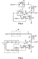
- FIG. 4 is a block/schematic diagram of one possible embodiment of a voltage boost circuit per the present invention.
- FIG. 5 is a schematic diagram of one possible implementation of the voltage boost circuit shown in FIG. 4 .
- FIG. 6 is a timing diagram which illustrates the operation of the voltage boost circuits of FIGS. 4 and 5 .
- FIG. 7 is a block/schematic diagram of another possible embodiment of a voltage boost circuit per the present invention.
- FIG. 8 is a timing diagram which illustrates the operation of the voltage boost circuit of FIG. 7 .
- FIG. 9 is a block/schematic diagram of another possible embodiment of a voltage boost circuit per the present invention.
- FIG. 10 is a timing diagram which illustrates the operation of the voltage boost circuit of FIG. 9 .
- FIG. 1 The basic principles of a voltage boost circuit in accordance with the present invention are illustrated in FIG. 1 and the accompanying timing diagram shown in FIG. 2 .
- the present voltage boost circuit is driven with a clock signal CLK, which toggles between a first voltage V 1 and a second voltage V 2 , where V 1 ⁇ V 2 .
- V 1 and V 2 would typically be available supply voltages on the IC on which the present circuit resided; in the example shown, V 2 is the IC's positive supply voltage VDD and V 1 is ground, though other values—including a non-zero V 1 value—could also be used.
- the circuit includes an output node OUT, at which the boosted voltage is provided.
- a first MOSFET MP 1 is coupled between CLK and OUT, and a second MOSFET MP 2 is coupled between OUT and ground (though a non-zero voltage could also be used).
- Each of the MOSFETs is fabricated with a ‘well’ process, which provides a well in which the MOSFET's drain, source and bulk regions reside. Thus, the PMOS FETs used in this exemplary embodiment are made with an nwell process.
- the first terminal 12 of a capacitance C is coupled to output node OUT.
- the voltage applied to the top (clock signal side) of MP 1 toggles between ⁇ VDD and ground in response to the first clock signal.
- a delay circuit 14 is coupled to the second terminal 16 of capacitance C, and arranged to toggle the voltage on the second terminal to ⁇ VDD or ground a predetermined amount of time after the voltage applied to the top of MP 1 toggles to ⁇ VDD or ground, respectively.
- the voltage boost circuit When arranged as shown in FIGS. 1 and 2 , the voltage boost circuit operates as follows:
- the bulk terminals of MP 1 ( 18 ) and MP 2 ( 20 ) are both connected to OUT.
- the well-substrate junctions of MP 1 and MP 2 are subjected to a voltage greater than VDD or less than ground.
- the more robust nwell-substrate junctions for these PMOS FETs are exposed to the boosted voltages, neither MP 1 or MP 2 is overstressed.
- FIG. 3 is a sectional diagram of a PMOS FET as employed herein.
- an nwell 30 is fabricated within a P-type substrate 32 .
- the device's source and bulk terminals are connected together, and to output node OUT.
- Substrate 32 is at ground.
- nwell 30 effectively serves as the FET's substrate.
- both the source and bulk terminals being at the boosted voltage (>VDD), there is essentially 0 volts across the source-nwell junction. As such, the source terminal is not stressed.
- the boosted voltage is only present across the nwell-substrate junction, which is the most capable of accommodating the boosted voltage.
- FIG. 4 A more practical realization of the present boost circuit is shown in FIG. 4 .
- PMOS FET MP 1 is connected between a clock signal (here, identified as “CLK1”) and output node OUT
- PMOS FET MP 2 is connected between OUT and ground
- the first terminal 12 of capacitance C is connected to OUT
- the bulk terminals of MP 1 and MP 2 are also connected to OUT.
- delay circuit 14 connected in series with the second terminal 16 of capacitance C
- MP 2 and delay circuit 14 are here driven by the output of an inverter 42 , which is driven with a second clock signal CLK2.
- Delay circuits 14 and 40 could be implemented in many different ways. One possible way is simply to use inverters, as shown in FIG. 5 .
- FIGS. 4 and 5 The operation of a voltage boost circuit as shown in FIGS. 4 and 5 is illustrated with reference to the timing diagram shown in FIG. 6 .
- the voltages at nodes X (drain side of MP 1 ), Y (gate of MP 2 ), and W (output of delay circuit 14 ) are shown in FIG. 6 , along with CLK1, CLK2, and OUT.
- CLK1 and CLK2 are inverses of each other, and preferably non-overlapping such that they are never high at the same time.
- the diagram assumes that CLK1 and CLK2 toggle between V 1 and V 2 , with V 1 being ground and V 2 being a VDD voltage of 5 volts.
- the voltage boost circuit When arranged as shown in FIGS. 4 and 5 , the voltage boost circuit operates as follows:
- the voltage boost circuit is preferably arranged such that, when CLK1 toggles from V 1 to V 2 , node ‘Y’ rises before node ‘X’. This is because if ‘X’ rose before ‘Y’, MP 2 would still be on and current would be conducted from ‘X’ to ground via MP 2 , thereby wasting current and degrading efficiency. Similarly, when CLK1 toggles from V 2 to V 1 , node ‘X’ should fall before node ‘Y’, to avoid current being conducted from ‘X’ to ground via MP 2 . These relationships can be ensured with the use of non-overlapping clocks as described above. The delay times associated with delay circuits 14 and 40 should be selected so that the events described above transpire in the proper order, and to allow necessary settling to occur.
- FIG. 7 is a block/schematic diagram of another possible embodiment of a voltage boost circuit per the present invention.
- the circuit is driven with a clock signal CLK.
- CLK is applied to a MOSFET MP 3 via an inverter 50 , with the other side of MP 3 connected to an output node OUT and the first terminal of a capacitance C.
- CLK is also coupled to a delay circuit 54 , the output of which is coupled to the second terminal 56 of capacitance C via an inverter 58 ; as above, delay circuit 54 could be implemented with one or more inverters connected in series, or by any of a number of other means.
- a logic gate 60 a NAND gate in this example, is connected to CLK and second terminal 56 at its inputs, with its output connected to the gate of MP 3 .
- One or more MOSFETs are connected between OUT and a supply voltage—four are shown in this example: MP 4 , MP 5 , MP 6 and MP 7 , connected between VDD and OUT.
- FIG. 7 The operation of a voltage boost circuit as shown in FIG. 7 is illustrated with reference to the timing diagram shown in FIG. 8 .
- the voltages at nodes X (drain side of MP 3 ), Y (second terminal of C), and W (output of logic gate 60 ) are shown in FIG. 8 , along with CLK and OUT.
- the diagram assumes that the circuit is connected between a positive supply voltage (VDD) of 5 volts and ground.
- VDD positive supply voltage
- the voltage at OUT is increased to a voltage greater than VDD when the output of inverter 58 (‘Y’) by way of delay circuit 54 toggles to ⁇ VDD a predetermined amount of time after the voltage applied to D 1 (‘X’) toggles to VDD (region ‘B’).
- the voltage greater than VDD is limited by the threshold voltage of MP 3 , which conducts when OUT exceeds VDD+V t,MP3 , where V t,MP3 is the threshold voltage of MP 3 .
- Output node OUT remains above VDD until the next transition of CLK.
- the voltage at node Y falls a predetermined amount of time after CLK toggles to VDD. This causes OUT to be further pulled down (region ‘D’).
- the negative excursion of OUT is limited by the gate-source voltages of FETs MP 4 -MP 7 ; this limiting circuit could be set so that, when low, OUT is either above or below ground potential.
- MP 4 -MP 7 be implemented with MOSFETs; for example, p-n junction diodes might be used instead, in which case the negative excursion of OUT is limited by the voltage drops across the diodes.
- the bulk terminals of MP 3 and MP 4 are connected to OUT, and only the nwell-substrate junctions of MP 3 and MP 4 are subjected to a voltage greater than VDD; no transistor is stressed beyond its rated voltage limits.
- the circuit of FIG. 7 is preferably arranged such that, when CLK toggles from VDD to ground, the delay imposed by delay circuit 54 is such that node X rises before node Y by an amount of time sufficient to allow capacitance C to charge up to ⁇ VDD-V MP3 .
- the delay imposed by delay circuit 54 should be sufficient to allow MP 3 to be turned on and C to discharge to ⁇ V t,MP3 before node Y falls.
- the delay time associated with delay circuit 54 should be selected so that the events described above transpire in the proper order, and to allow necessary settling to occur.
- FIG. 9 Another possible embodiment of a voltage boost circuit per the present invention is shown in FIG. 9 .
- This embodiment is similar to that shown in FIG. 7 , but has several additions and modifications.
- the present boost circuit can employ different types of logic gates; this embodiment is configured so that the logic gate is an XOR gate 70 .
- the clamps which limit the negative excursion of OUT can have any of a number of different configurations; for example, here, the clamps are reduced in number to three (MP 8 -MP 10 ), and have their bulk terminals tied to their sources.
- This embodiment also includes inverters 72 and 74 , with the ground side of inverter 74 connected to ground through a resistor 76 , and a switch 78 connected across the resistor. These components act to limit the undershoot of the OUT signal at its falling edge, because resistor 76 limits the rate of fall at node Y (at the end of region ‘C’ in FIG. 8 ). During charging of capacitor C (region ‘A’), resistor 76 is shorted out by switch 78 , thereby allowing fast charging.
- FIG. 10 A timing diagram for the embodiment of FIG. 9 is shown in FIG. 10 .
- the diagram is essentially the same as that shown in FIG. 8 , except that signal W now has an additional low pulse during the duration of region ‘A’.
- FIGS. 1 , 4 , 5 , 7 and 9 are merely exemplary. It is only essential that voltages be switched across a capacitance as needed to provide a boosted output voltage, with the circuitry arranged such that the only active device junctions subjected to the boosted voltages are the devices' well-substrate junctions.
Landscapes
- Engineering & Computer Science (AREA)
- Power Engineering (AREA)
- Microelectronics & Electronic Packaging (AREA)
- Logic Circuits (AREA)
- Dc-Dc Converters (AREA)
Abstract
Description
-
- the capacitance and thereby the output node is initially charged to ˜V2 when the voltage applied to the top of the first MOSFET toggles to ˜V2 in response to the clock signal, and
- the output node voltage is increased to a voltage greater than V2 when the output of the delay circuit toggles to ˜V2 the predetermined amount of time after the voltage applied to the top of the first MOSFET toggles to ˜V2.
-
- when CLK toggles to VDD, MP2 will be off, the drain of MP1 will be pulled up to VDD, and the source of MP1 will be at about VDD-VMP1, where VMP1 is the voltage drop across MP1. The voltage on
second capacitance terminal 16 is low, so that C gets charged up to VDD-VMP1. This is shown as region ‘A’ inFIG. 2 . - when the output of
delay circuit 14 toggles to ˜VDD the predetermined amount of time after the voltage applied to the top of MP1 toggles to ˜VDD, the voltage at OUT is increased to a voltage greater than VDD (region ‘B’). The amount by which OUT exceeds VDD is limited by the gate-source voltage (Vgs) of MP2 to about 1 volt above MP2's gate voltage. MP2's gate voltage is at VDD during this interval; thus, OUT is limited by MP2 to about VDD+1v. - when CLK toggles low, the drain of MP1 and the gate of MP2 go to ground. This turns MP2 on and pulls down the voltage at OUT (region ‘C’).
- when the output of
delay circuit 14 toggles to ground the predetermined amount of time after the voltage applied to the top of MP1 toggles to ground, the voltage at OUT is pulled below ground (region ‘D’). The amount by which OUT is less than ground is limited by the intrinsic nwell-substrate diode of MP1 to about −1 volt.
- when CLK toggles to VDD, MP2 will be off, the drain of MP1 will be pulled up to VDD, and the source of MP1 will be at about VDD-VMP1, where VMP1 is the voltage drop across MP1. The voltage on
-
- when CLK1 toggles to VDD, CLK2 is low, ‘Y’ is high, and MP2 is off.
Delay circuit 40 delays the application of CLK1 to MP1 by a predetermined amount of time. At the end of the predetermined amount of time, the drain of MP1 (‘X’) is pulled up to VDD, and the source of MP1 will be at about VDD-VMP1, where VMP1 is the voltage drop across MP1. The voltage oncapacitance terminal 16 is low, so that C gets charged up to VDD-VMP1. This is shown as region ‘A’ inFIG. 6 . - delay
circuit 14 delays the application ofCLK2 (‘Y’) to C for a predetermined amount of time after the voltage applied tofirst terminal 12 via MP1 toggles to VDD-VMP1. When the output of delay circuit 14 (‘W’) toggles to ˜VDD, the voltage at OUT is increased to a voltage greater than VDD (region ‘B’). As before, the amount by which OUT exceeds VDD is limited by the Vgs of MP2 to about VDD+1v. - when CLK1 toggles low, the drain of MP1 (‘X’) falls to ground. Then, when CLK2 toggles high, the gate of MP2 {‘Y’} goes to ground, which turns MP2 on and pulls down the voltage at OUT (region ‘C’).
- when the output of delay circuit 14 (‘W’) toggles to ground the predetermined amount of time after the voltage applied to
first terminal 12 via MP1 toggles to ground, the voltage at OUT is pulled below ground (region ‘D’). The amount by which OUT is less than ground is limited by the intrinsic nwell-substrate diode of MP1 to about −1 volt.
- when CLK1 toggles to VDD, CLK2 is low, ‘Y’ is high, and MP2 is off.
Claims (26)
Priority Applications (2)
| Application Number | Priority Date | Filing Date | Title |
|---|---|---|---|
| US12/154,950 US8253477B2 (en) | 2008-05-27 | 2008-05-27 | Voltage boost circuit without device overstress |
| PCT/US2009/003026 WO2009145872A1 (en) | 2008-05-27 | 2009-05-14 | Voltage boost circuit without device overstress |
Applications Claiming Priority (1)
| Application Number | Priority Date | Filing Date | Title |
|---|---|---|---|
| US12/154,950 US8253477B2 (en) | 2008-05-27 | 2008-05-27 | Voltage boost circuit without device overstress |
Publications (2)
| Publication Number | Publication Date |
|---|---|
| US20090295362A1 US20090295362A1 (en) | 2009-12-03 |
| US8253477B2 true US8253477B2 (en) | 2012-08-28 |
Family
ID=40812506
Family Applications (1)
| Application Number | Title | Priority Date | Filing Date |
|---|---|---|---|
| US12/154,950 Active 2031-02-02 US8253477B2 (en) | 2008-05-27 | 2008-05-27 | Voltage boost circuit without device overstress |
Country Status (2)
| Country | Link |
|---|---|
| US (1) | US8253477B2 (en) |
| WO (1) | WO2009145872A1 (en) |
Families Citing this family (3)
| Publication number | Priority date | Publication date | Assignee | Title |
|---|---|---|---|---|
| CN102684462B (en) * | 2012-05-31 | 2014-06-18 | 安徽工业大学 | Novel low end metal oxide semiconductor field effect transistor (MOSFET)/ insulated gate bipolar transistor (IGBT) negative pressure clamping driving circuit and control method thereof |
| US8816748B2 (en) | 2012-06-12 | 2014-08-26 | Lsi Corporation | Jitter reduction in high speed low core voltage level shifter |
| US10277117B2 (en) * | 2017-05-23 | 2019-04-30 | Taiwan Semiconductor Manufacturing Company Limited | Device with a voltage multiplier |
Citations (11)
| Publication number | Priority date | Publication date | Assignee | Title |
|---|---|---|---|---|
| US4016476A (en) | 1972-09-20 | 1977-04-05 | Citizen Watch Co., Ltd. | Booster circuits |
| US4259686A (en) | 1977-10-03 | 1981-03-31 | Tokyo Shibaura Denki Kabushiki Kaisha | Circuit for producing a polarity-reversed voltage with opposite polarity to that of a power supply voltage |
| US5563548A (en) * | 1994-08-24 | 1996-10-08 | Hyundai Electronics Industries Co., Ltd. | Output voltage controlling circuit in a negative charge pump |
| JPH09297997A (en) | 1996-05-02 | 1997-11-18 | Toshiba Corp | Nonvolatile semiconductor memory |
| US6118326A (en) | 1997-11-06 | 2000-09-12 | Analog Devices, Inc. | Two-phase bootstrapped CMOS switch drive technique and circuit |
| US6326774B1 (en) * | 1999-08-26 | 2001-12-04 | Texas Instruments Deutschland, Gmbh | Step-up DC voltage converter and method of operation |
| US6356137B1 (en) * | 2000-06-26 | 2002-03-12 | Fairchild Semiconductor Corporation | Voltage boost circuit with low power supply voltage |
| US20030057469A1 (en) | 2001-08-01 | 2003-03-27 | Satoru Karaki | Semiconductor charge pump circuit and nonvolatile semiconductor memory device |
| US6828850B2 (en) | 2001-10-19 | 2004-12-07 | Clare Micronix Integrated Systems, Inc. | Method and system for charge pump active gate drive |
| US7271626B1 (en) * | 2004-10-27 | 2007-09-18 | National Semiconductor Corporation | Suppression of parasitic ringing at the output of a switched capacitor DC/DC converter |
| US7521978B2 (en) * | 2005-11-02 | 2009-04-21 | Hynix Semiconductor Inc. | Clock driver |
-
2008
- 2008-05-27 US US12/154,950 patent/US8253477B2/en active Active
-
2009
- 2009-05-14 WO PCT/US2009/003026 patent/WO2009145872A1/en active Application Filing
Patent Citations (11)
| Publication number | Priority date | Publication date | Assignee | Title |
|---|---|---|---|---|
| US4016476A (en) | 1972-09-20 | 1977-04-05 | Citizen Watch Co., Ltd. | Booster circuits |
| US4259686A (en) | 1977-10-03 | 1981-03-31 | Tokyo Shibaura Denki Kabushiki Kaisha | Circuit for producing a polarity-reversed voltage with opposite polarity to that of a power supply voltage |
| US5563548A (en) * | 1994-08-24 | 1996-10-08 | Hyundai Electronics Industries Co., Ltd. | Output voltage controlling circuit in a negative charge pump |
| JPH09297997A (en) | 1996-05-02 | 1997-11-18 | Toshiba Corp | Nonvolatile semiconductor memory |
| US6118326A (en) | 1997-11-06 | 2000-09-12 | Analog Devices, Inc. | Two-phase bootstrapped CMOS switch drive technique and circuit |
| US6326774B1 (en) * | 1999-08-26 | 2001-12-04 | Texas Instruments Deutschland, Gmbh | Step-up DC voltage converter and method of operation |
| US6356137B1 (en) * | 2000-06-26 | 2002-03-12 | Fairchild Semiconductor Corporation | Voltage boost circuit with low power supply voltage |
| US20030057469A1 (en) | 2001-08-01 | 2003-03-27 | Satoru Karaki | Semiconductor charge pump circuit and nonvolatile semiconductor memory device |
| US6828850B2 (en) | 2001-10-19 | 2004-12-07 | Clare Micronix Integrated Systems, Inc. | Method and system for charge pump active gate drive |
| US7271626B1 (en) * | 2004-10-27 | 2007-09-18 | National Semiconductor Corporation | Suppression of parasitic ringing at the output of a switched capacitor DC/DC converter |
| US7521978B2 (en) * | 2005-11-02 | 2009-04-21 | Hynix Semiconductor Inc. | Clock driver |
Non-Patent Citations (2)
| Title |
|---|
| Baker, R. Jacob; "CMOS Mixed-Signal Circuit Design"; The Institute of Electrical and Electronics Engineers, Inc.; 2002; pp. 260-261. |
| PCT Notification of the International Search Report and the Written Opinion of the International Searching Authority, Dated Jul. 27, 2009; for International Application No. PCT/US2009/003026. |
Also Published As
| Publication number | Publication date |
|---|---|
| US20090295362A1 (en) | 2009-12-03 |
| WO2009145872A1 (en) | 2009-12-03 |
Similar Documents
| Publication | Publication Date | Title |
|---|---|---|
| US9385596B1 (en) | Charge pump circuit capable of reducing reverse currents | |
| KR101225399B1 (en) | Step-down switching regulator | |
| US7176742B2 (en) | Bootstrapped switch with an input dynamic range greater than supply voltage | |
| JP4849907B2 (en) | Charge pump circuit | |
| US7274227B2 (en) | Power-on reset circuit | |
| US8456225B1 (en) | Negative charge pump | |
| US20090015974A1 (en) | Esd detection circuit | |
| US6208197B1 (en) | Internal charge pump voltage limit control | |
| US6670841B2 (en) | Level shifting circuit | |
| US20090015318A1 (en) | Charge pump drive circuit | |
| US20210184667A1 (en) | Semiconductor integrated circuit and control method of semiconductor integrated circuit | |
| US20090072891A1 (en) | Varactor-based charge pump | |
| US9800153B2 (en) | Negative voltage generator | |
| US8253477B2 (en) | Voltage boost circuit without device overstress | |
| CN109427371B (en) | Power switch, memory device and method for providing power switch voltage output | |
| US7692479B2 (en) | Semiconductor integrated circuit device including charge pump circuit capable of suppressing noise | |
| US7295056B2 (en) | Level shift circuit | |
| US8742829B2 (en) | Low leakage digital buffer using bootstrap inter-stage | |
| US11418188B1 (en) | Bootstrapped switch | |
| US7312650B2 (en) | Step-down voltage output circuit | |
| KR20060053977A (en) | Semiconductor integrated circuit and boosting method | |
| Bîzîitu et al. | On-chip 500μA dual-chain Dickson charge pump optimized for NMOS LDO supply | |
| JP5226474B2 (en) | Semiconductor output circuit | |
| US6828830B2 (en) | Low power, area-efficient circuit to provide clock synchronization | |
| EP2775621A1 (en) | A Dickson charge pump circuit |
Legal Events
| Date | Code | Title | Description |
|---|---|---|---|
| AS | Assignment |
Owner name: ANALOG DEVICES, INC.,MASSACHUSETTS Free format text: ASSIGNMENT OF ASSIGNORS INTEREST;ASSIGNORS:DOUTS, BENJAMIN A.;WAN, QUAN;REEL/FRAME:021057/0575 Effective date: 20080522 Owner name: ANALOG DEVICES, INC., MASSACHUSETTS Free format text: ASSIGNMENT OF ASSIGNORS INTEREST;ASSIGNORS:DOUTS, BENJAMIN A.;WAN, QUAN;REEL/FRAME:021057/0575 Effective date: 20080522 |
|
| STCF | Information on status: patent grant |
Free format text: PATENTED CASE |
|
| FPAY | Fee payment |
Year of fee payment: 4 |
|
| MAFP | Maintenance fee payment |
Free format text: PAYMENT OF MAINTENANCE FEE, 8TH YEAR, LARGE ENTITY (ORIGINAL EVENT CODE: M1552); ENTITY STATUS OF PATENT OWNER: LARGE ENTITY Year of fee payment: 8 |
|
| MAFP | Maintenance fee payment |
Free format text: PAYMENT OF MAINTENANCE FEE, 12TH YEAR, LARGE ENTITY (ORIGINAL EVENT CODE: M1553); ENTITY STATUS OF PATENT OWNER: LARGE ENTITY Year of fee payment: 12 |