US8144110B2 - Liquid crystal display and backlight system with detection circuit for detecting connection state of power input - Google Patents
Liquid crystal display and backlight system with detection circuit for detecting connection state of power input Download PDFInfo
- Publication number
- US8144110B2 US8144110B2 US12/154,759 US15475908A US8144110B2 US 8144110 B2 US8144110 B2 US 8144110B2 US 15475908 A US15475908 A US 15475908A US 8144110 B2 US8144110 B2 US 8144110B2
- Authority
- US
- United States
- Prior art keywords
- circuit
- light emitting
- emitting diode
- liquid crystal
- gate
- Prior art date
- Legal status (The legal status is an assumption and is not a legal conclusion. Google has not performed a legal analysis and makes no representation as to the accuracy of the status listed.)
- Active, expires
Links
Images


Classifications
-
- G—PHYSICS
- G02—OPTICS
- G02F—OPTICAL DEVICES OR ARRANGEMENTS FOR THE CONTROL OF LIGHT BY MODIFICATION OF THE OPTICAL PROPERTIES OF THE MEDIA OF THE ELEMENTS INVOLVED THEREIN; NON-LINEAR OPTICS; FREQUENCY-CHANGING OF LIGHT; OPTICAL LOGIC ELEMENTS; OPTICAL ANALOGUE/DIGITAL CONVERTERS
- G02F1/00—Devices or arrangements for the control of the intensity, colour, phase, polarisation or direction of light arriving from an independent light source, e.g. switching, gating or modulating; Non-linear optics
- G02F1/01—Devices or arrangements for the control of the intensity, colour, phase, polarisation or direction of light arriving from an independent light source, e.g. switching, gating or modulating; Non-linear optics for the control of the intensity, phase, polarisation or colour
- G02F1/13—Devices or arrangements for the control of the intensity, colour, phase, polarisation or direction of light arriving from an independent light source, e.g. switching, gating or modulating; Non-linear optics for the control of the intensity, phase, polarisation or colour based on liquid crystals, e.g. single liquid crystal display cells
- G02F1/133—Constructional arrangements; Operation of liquid crystal cells; Circuit arrangements
- G02F1/1333—Constructional arrangements; Manufacturing methods
- G02F1/1335—Structural association of cells with optical devices, e.g. polarisers or reflectors
- G02F1/1336—Illuminating devices
- G02F1/133602—Direct backlight
- G02F1/133603—Direct backlight with LEDs
-
- G—PHYSICS
- G09—EDUCATION; CRYPTOGRAPHY; DISPLAY; ADVERTISING; SEALS
- G09G—ARRANGEMENTS OR CIRCUITS FOR CONTROL OF INDICATING DEVICES USING STATIC MEANS TO PRESENT VARIABLE INFORMATION
- G09G3/00—Control arrangements or circuits, of interest only in connection with visual indicators other than cathode-ray tubes
- G09G3/20—Control arrangements or circuits, of interest only in connection with visual indicators other than cathode-ray tubes for presentation of an assembly of a number of characters, e.g. a page, by composing the assembly by combination of individual elements arranged in a matrix no fixed position being assigned to or needed to be assigned to the individual characters or partial characters
- G09G3/34—Control arrangements or circuits, of interest only in connection with visual indicators other than cathode-ray tubes for presentation of an assembly of a number of characters, e.g. a page, by composing the assembly by combination of individual elements arranged in a matrix no fixed position being assigned to or needed to be assigned to the individual characters or partial characters by control of light from an independent source
- G09G3/3406—Control of illumination source
-
- G—PHYSICS
- G02—OPTICS
- G02F—OPTICAL DEVICES OR ARRANGEMENTS FOR THE CONTROL OF LIGHT BY MODIFICATION OF THE OPTICAL PROPERTIES OF THE MEDIA OF THE ELEMENTS INVOLVED THEREIN; NON-LINEAR OPTICS; FREQUENCY-CHANGING OF LIGHT; OPTICAL LOGIC ELEMENTS; OPTICAL ANALOGUE/DIGITAL CONVERTERS
- G02F1/00—Devices or arrangements for the control of the intensity, colour, phase, polarisation or direction of light arriving from an independent light source, e.g. switching, gating or modulating; Non-linear optics
- G02F1/01—Devices or arrangements for the control of the intensity, colour, phase, polarisation or direction of light arriving from an independent light source, e.g. switching, gating or modulating; Non-linear optics for the control of the intensity, phase, polarisation or colour
- G02F1/13—Devices or arrangements for the control of the intensity, colour, phase, polarisation or direction of light arriving from an independent light source, e.g. switching, gating or modulating; Non-linear optics for the control of the intensity, phase, polarisation or colour based on liquid crystals, e.g. single liquid crystal display cells
- G02F1/133—Constructional arrangements; Operation of liquid crystal cells; Circuit arrangements
- G02F1/1333—Constructional arrangements; Manufacturing methods
- G02F1/1335—Structural association of cells with optical devices, e.g. polarisers or reflectors
- G02F1/1336—Illuminating devices
- G02F1/133602—Direct backlight
- G02F1/133612—Electrical details
-
- G—PHYSICS
- G09—EDUCATION; CRYPTOGRAPHY; DISPLAY; ADVERTISING; SEALS
- G09G—ARRANGEMENTS OR CIRCUITS FOR CONTROL OF INDICATING DEVICES USING STATIC MEANS TO PRESENT VARIABLE INFORMATION
- G09G2330/00—Aspects of power supply; Aspects of display protection and defect management
- G09G2330/02—Details of power systems and of start or stop of display operation
- G09G2330/027—Arrangements or methods related to powering off a display
Definitions
- the present invention relates to backlight systems and liquid crystal display devices, and particularly to a backlight system with a detection circuit and a liquid crystal display device using the backlight system.
- a typical liquid crystal display (LCD) device has the advantages of portability, low power consumption, and low radiation, and has been widely used in various portable information products such as notebooks, personal digital assistants (PDAs), video cameras and the like. Furthermore, the LCD is considered by many to have the potential to completely replace CRT (cathode ray tube) monitors and televisions.
- CTR cathode ray tube
- One kind of conventional LCD device includes an LCD panel, a backlight source for illuminating the LCD panel, and a power supply circuit for driving the LCD panel and the light source.
- the LCD device 1 includes an alternating current (AC) filter circuit 11 , a rectifier and voltage step-down circuit 12 , an LCD panel 13 , a scaler 14 , an LED driving circuit 15 , and an LED array 16 .
- AC alternating current
- the AC filter circuit 11 generally includes capacitors with large capacitance and windings with large inductance, in order to filter surge voltages from an external electrical network, and then output steady AC current to the rectifier and voltage step-down circuit 12 . Then the AC current is rectified and reduced to variety of direct current (DC) voltages, such as 3 volts (V), 5V, 9V, and the like. The DC voltages are used for driving the LCD panel 13 and the scaler 14 .
- DC direct current
- the scaler 14 receives video signals from an external device, processes the video signals, and then sends the video signals to the LCD panel 13 for display of corresponding images. At the same time, the scaler 14 outputs a pulse width modulation (PWM) signal to the LED driving circuit 15 .
- PWM pulse width modulation
- the LED driving circuit 15 receives the PWM signal, and correspondingly drives the LED array 16 to emit light beams for illuminating the LCD panel 13 .
- the AC filter circuit 11 and the rectifier and voltage step-down circuit 12 both include large capacitors and large windings. In operation, electrical power is stored in the capacitors and the windings. However, when the AC power is cut off, electrical power stored in the capacitors and the windings is released. The released electrical power drives the LCD panel 13 and the LED array 16 to continue working for a moment after the AC power is cut off. Because the released power is abnormal and uncontrolled, colors displayed on the LCD panel 13 are correspondingly abnormal and uncontrolled. For example, so-called red and blue noise colors are displayed. The noise colors reduce a display quality and aesthetic appeal of the LCD device 1 .
- a backlight system in a first aspect, includes a power input circuit a detection circuit, a control circuit, a light emitting diode driving circuit, and a light emitting diode array.
- the detection circuit is configured to detect a connection state of the power input circuit with respect to an external power source, and send a corresponding connection states signal to the control circuit.
- the control circuit is configured to output a control signal to the light emitting diode driving circuit according to the connection state signal.
- the light emitting diode driving circuit is configured to drive or shut down the light emitting diode array according to the control signal.
- a liquid crystal display device in a second aspect, includes a power input circuit, a detection circuit, a control circuit, a light emitting diode driving circuit, a light emitting diode array, a scaler, and a liquid crystal display panel.
- the power input circuit is capable of receiving electrical power from an external power source and providing electrical power to the liquid crystal display panel and the scaler.
- the scaler is configured to provide video signals to the liquid crystal display panel.
- the detection circuit is configured to detect a connection state of the power input circuit with respect to an external power source, and send a corresponding connection state signal to the control circuit, the control circuit is configured to output a control signal to the light emitting diode driving circuit according to the connection state signal.
- the light emitting diode driving circuit is configured to switch driving of the light emitting diode array according to the control signal.
- a liquid crystal display device in a third aspect, includes a power input circuit, a liquid crystal panel, a scaler configured for providing video signals to the liquid crystal display panel, and a backlight system configured for providing light beams for the liquid crystal display panel.
- the power input circuit is capable of receiving alternating current from an external power source and providing direct current to the liquid crystal display panel and the scaler
- the backlight system is coupled to the power input circuit and is configured to detect a connection state of the power input circuit with respect to an external power source, and is further configured to provide or stop providing light beams to illuminate the liquid crystal display panel according to the connection state detected by the power input circuit.
- FIG. 1 is a block diagram of an LCD device according to a preferred embodiment of the present invention.
- FIG. 2 is a circuit diagram of a portion of the LCD device marked by dashed lines in FIG. 1 .
- FIG. 3 is a block diagram of a conventional LCD device.
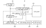
- FIG. 1 is a block diagram of an LCD device according to a preferred embodiment of the present invention.
- the LCD device 2 includes an AC filter circuit 21 , a rectifier and voltage step-down circuit 22 , an LCD panel 23 , a scaler 24 , an AC detection circuit 27 , an LED driving control circuit 28 , an LED driving circuit 25 , and an LED array 26 .
- the AC filter circuit 21 generally includes capacitors with large capacitance and windings with large inductance.
- the AC filter circuit 21 receives AC voltage from an external electrical network, and filters surge voltages and electromagnetic interference (EMI) of the external electrical network.
- EMI electromagnetic interference
- the LCD device 2 thereby complies with relevant Federal Communication Commission (FCC) standards, European Community (CE) standards, and the like. Then the AC filter circuit 21 outputs steady AC voltage to the rectifier and voltage step-down circuit 22 .
- FCC Federal Communication Commission
- CE European Community
- the rectifier and voltage step-down circuit 22 generally includes a rectifier circuit (not shown) and a DC-DC voltage step-down circuit (not shown).
- the rectifier circuit transforms the AC voltage to a high DC voltage.
- the DC-DC voltage step-down circuit reduces the high DC voltage to a variety of low DC voltages, such as 3V (volts), 5V, 9V, 12V, and the like. Then the low DC voltages are supplied to the LCD panel 23 and the scaler 24 .
- the scaler 24 receives video signals such as low voltage differential signals (LVDS), processes the video signals, and sends the video signals to the LCD panel 23 . At the same time, the scaler 24 outputs a PWM signal to the LED driving control circuit 28 .
- video signals such as low voltage differential signals (LVDS)
- LVDS low voltage differential signals
- the AC detection circuit 27 is coupled to an output of the AC filter circuit 21 .
- the AC detection circuit 27 is capable of sampling the AC voltage of the AC filter circuit 21 , in order to detect whether the AC filter circuit 21 is connected to an external electrical network. Then the AC detection circuit 27 outputs a corresponding connection state signal to the LED driving control circuit 28 .
- the connection state signal indicates that the AC filter circuit 21 is connected to an external electrical network, or that the AC filter circuit 21 is not connected to an external electrical network.
- the LED driving control circuit 28 receives signals from both the AC detection circuit 27 and the scaler 24 , analyzes the signals, and outputs appropriate control signals to the LED driving circuit 25 . Then the LED driving circuit 25 outputs voltage to turn on or turn off the LED array 26 according to the control signals from the LED driving control circuit 28 .
- the AC detection circuit 27 detects the output of the AC filter circuit 21 , and sends a first signal to the LED driving control circuit 28 .
- the LED driving control circuit 28 Under the control of the first signal from the AC detection circuit 27 and the PWM signal from the scaler 24 , the LED driving control circuit 28 sends a switch-on signal to the LED driving circuit 25 . Then the LED driving circuit 25 outputs a high voltage to switch on the LED array 26 for illuminating the LCD panel 23 .
- the AC detection circuit 27 Upon a condition that the AC filter circuit 21 is disconnected or cut off from an external electrical network, the AC detection circuit 27 detects that no AC voltage is sent out from the AC filter circuit 21 . Then the AC detection circuit 27 sends a second signal to the LED driving control circuit 28 . Under the control of the second signal from the AC detection circuit 27 and the PWM signal from the scaler 24 , the LED driving control circuit 28 sends a switch-off signal to the LED driving circuit 25 . Accordingly, the LED driving circuit 25 outputs a low voltage to switch off the LED array 26 . Thus, once the LCD device 2 is cut off from the external electrical network, the backlight provided by the LED array 26 is switched off immediately without any time delay.
- the marked portion includes the scaler 24 , the LED driving circuit 25 , the LED array 26 , the AC detection circuit 27 , and the LED driving control circuit 28 .
- the AC detection circuit 27 includes an AC detection terminal 270 , a first resistor 271 , a second resistor 272 , a diode 273 , a capacitor 275 , and a transistor 276 .
- the AC detection terminal 270 is connected to the output of the AC filter circuit 21 for detecting the AC voltage.
- the AC detection terminal 270 , the first resistor 271 , and the second resistor 273 are connected in series to ground.
- a positive electrode of the diode 273 is connected to a node between the first resistor 271 and the second resistor 272 .
- the capacitor 275 is connected between a negative electrode of the diode 273 and ground.
- the transistor 276 is a positive-negative-positive (PNP) type bipolar junction transistor, which includes a base “b”, an emitter “e”, and a collector “c”.
- the base “b” is connected to the negative electrode of the diode 273 .
- the emitter “e” is connected to a constant DC power supply, such as a 3.3 V DC power supply.
- the scaler 24 includes an output pin 241 for outputting the PWM signal.
- the LED driving control circuit 28 includes a NOT gate 281 , and an AND gate 283 with two input terminals. An input terminal of the NOT gate 281 is connected to the collector “c” of the transistor 276 . An output terminal of the NOT gate 281 is connected to a first input terminal of the AND gate 283 . A second input terminal of the AND gate 283 is connected to the output pin 241 of the scaler 24 .
- the LED driving circuit 25 includes an LED driver IC 250 .
- the LED driver IC 250 can for example be a G5950 model, which includes a control signal input pin DIM and eight output pins CH 1 ⁇ CH 8 .
- the control signal input pin DIM is connected to an output of the AND gate 28 .
- the eight output pins CH 1 ⁇ CH 8 are connected to the LED array 26 for supplying driving voltages thereto.
- the output pins CH 1 ⁇ CH 8 output high voltage to switch on the LED array 26 .
- the output pins CH 1 ⁇ CH 8 output low voltage to switch off the LED array 26 .
- Typical detailed operation of the LCD device 2 is as follows:
- AC voltage output from the AC filter circuit 21 is sampled by the second resistor 272 .
- the diode 273 and the capacitor 275 function as a rectifier and filter circuit, which transforms the sampling AC voltage to a sampling DC voltage.
- the sampling DC voltage is supplied to the base “b” of the transistor 276 .
- the sampling DC voltage that is applied to the base “e” of the transistor 276 is a high voltage.
- the transistor 276 is switched off and the collector “c” outputs a low voltage.
- the low voltage is converted into a high voltage by the NOT gate 281 of the LED driving control circuit 28 .
- the output of the AND gate 283 is determined by the PWM signal from the output pin 241 .
- the output of the AND gate 283 is a high voltage.
- the LED driver IC 250 outputs high voltage at the output pins CH 1 ⁇ CH 8 .
- the LED array 26 is switched on and emits light beams. If the PWM signal is a low voltage, the output of the AND gate 283 is a low voltage.
- the LED driver IC 250 outputs low voltages at the output pins CH 1 ⁇ CH 8 .
- the LED array 26 is switched off.
- the sampling DC voltage that is applied to the base “e” of the transistor 276 is a low voltage.
- the transistor 276 is switched on and the collector “c” outputs a high voltage.
- the high voltage is converted into a low voltage by the NOT gate 281 of the LED driving control circuit 28 .
- the AND gate 283 outputs a low voltage to the control signal input pin DIM.
- the eight output pins CH 1 ⁇ CH 8 then output low voltages to the LED array 26 .
- the LED array 26 is switch off.
- the LCD device 2 includes the AC detection circuit 27 and the LED driving control circuit 28 .
- the AC detection circuit 27 samples an AC signal, and detects whether the AC filter circuit 21 is connected to an external electrical network. Upon a condition that the AC filter circuit 21 is cut off or disconnected from an external electrical network, the AC detection circuit 27 sends a cut-off signal to the LED driving control circuit 28 . With the cut-off signal, the LED driving control circuit 28 outputs a control signal to lower the output voltage of the LED driving circuit 25 . Therefore the LED array 26 is switched off immediately. Accordingly, once the LCD device 2 is cut off from the external electrical network, the LED array 26 stops emitting light beams. This reduces or even eliminates color noise when the AC filter circuit 21 is cut off from the external electrical network, and thereby improves a display quality and aesthetic appeal of the LCD device 2 .
Landscapes
- Physics & Mathematics (AREA)
- Nonlinear Science (AREA)
- Engineering & Computer Science (AREA)
- General Physics & Mathematics (AREA)
- Optics & Photonics (AREA)
- Crystallography & Structural Chemistry (AREA)
- Chemical & Material Sciences (AREA)
- Mathematical Physics (AREA)
- Computer Hardware Design (AREA)
- Theoretical Computer Science (AREA)
- Liquid Crystal Display Device Control (AREA)
- Control Of Indicators Other Than Cathode Ray Tubes (AREA)
- Liquid Crystal (AREA)
Abstract
Description
Claims (14)
Applications Claiming Priority (3)
| Application Number | Priority Date | Filing Date | Title |
|---|---|---|---|
| CN200710074605 | 2007-05-25 | ||
| CN200710074605.5 | 2007-05-25 | ||
| CN200710074605A CN100592152C (en) | 2007-05-25 | 2007-05-25 | Backlight system, liquid crystal display system adopting same and its drive method |
Publications (2)
| Publication Number | Publication Date |
|---|---|
| US20080291154A1 US20080291154A1 (en) | 2008-11-27 |
| US8144110B2 true US8144110B2 (en) | 2012-03-27 |
Family
ID=40071949
Family Applications (1)
| Application Number | Title | Priority Date | Filing Date |
|---|---|---|---|
| US12/154,759 Active 2030-11-16 US8144110B2 (en) | 2007-05-25 | 2008-05-27 | Liquid crystal display and backlight system with detection circuit for detecting connection state of power input |
Country Status (2)
| Country | Link |
|---|---|
| US (1) | US8144110B2 (en) |
| CN (1) | CN100592152C (en) |
Cited By (11)
| Publication number | Priority date | Publication date | Assignee | Title |
|---|---|---|---|---|
| US20130027370A1 (en) * | 2011-02-03 | 2013-01-31 | Manufacturing Resources International, Inc. | System and method for dynamic load sharing between electronic displays |
| US9799306B2 (en) | 2011-09-23 | 2017-10-24 | Manufacturing Resources International, Inc. | System and method for environmental adaptation of display characteristics |
| US9867253B2 (en) | 2008-05-21 | 2018-01-09 | Manufacturing Resources International, Inc. | Backlight adjustment system |
| US9924583B2 (en) | 2015-05-14 | 2018-03-20 | Mnaufacturing Resources International, Inc. | Display brightness control based on location data |
| US10185352B2 (en) | 2009-01-08 | 2019-01-22 | Manufacturing Resources International, Inc. | Modular system for controlling a liquid crystal display |
| US10578658B2 (en) | 2018-05-07 | 2020-03-03 | Manufacturing Resources International, Inc. | System and method for measuring power consumption of an electronic display assembly |
| US10586508B2 (en) | 2016-07-08 | 2020-03-10 | Manufacturing Resources International, Inc. | Controlling display brightness based on image capture device data |
| US10593255B2 (en) | 2015-05-14 | 2020-03-17 | Manufacturing Resources International, Inc. | Electronic display with environmental adaptation of display characteristics based on location |
| US10607520B2 (en) | 2015-05-14 | 2020-03-31 | Manufacturing Resources International, Inc. | Method for environmental adaptation of display characteristics based on location |
| US10782276B2 (en) | 2018-06-14 | 2020-09-22 | Manufacturing Resources International, Inc. | System and method for detecting gas recirculation or airway occlusion |
| US11526044B2 (en) | 2020-03-27 | 2022-12-13 | Manufacturing Resources International, Inc. | Display unit with orientation based operation |
Families Citing this family (8)
| Publication number | Priority date | Publication date | Assignee | Title |
|---|---|---|---|---|
| KR20090006142A (en) * | 2006-03-31 | 2009-01-14 | 코닌클리케 필립스 일렉트로닉스 엔.브이. | Display apparatus with ambient lighting generation using switchable canvas |
| KR101593939B1 (en) | 2009-10-23 | 2016-02-15 | 삼성전자 주식회사 | Display apparatus power supply apparatus and power supply method thereof |
| CN101958083A (en) * | 2010-06-02 | 2011-01-26 | 苏州工业园区胜欣电子有限公司 | Power supply device for advertising machine |
| US9257079B2 (en) * | 2011-06-27 | 2016-02-09 | Shenzhen China Star Optoelectronics Technology Co., Ltd. | Data driving system and chip for liquid crystal panel as well as liquid crystal display device |
| CN102955062B (en) * | 2011-08-29 | 2015-03-18 | 群康科技(深圳)有限公司 | Electronic device |
| CN105872431B (en) * | 2016-04-20 | 2019-03-12 | 武汉华星光电技术有限公司 | The noise detection device and noise detection method of display module |
| CN110880302A (en) * | 2019-12-05 | 2020-03-13 | 山东超越数控电子股份有限公司 | LCD screen anti-screen-splash system based on domestic processor and implementation method |
| CN112688739B (en) * | 2020-12-16 | 2022-08-09 | 武汉永鼎光通科技有限公司 | APC control circuit that self-adaptation is shaded |
Citations (9)
| Publication number | Priority date | Publication date | Assignee | Title |
|---|---|---|---|---|
| US5886880A (en) | 1997-05-28 | 1999-03-23 | Nec Corporation | Power circuit for transferring energy by alternately switching winding circuits of a transformer at high speed |
| US20020021275A1 (en) * | 2000-08-14 | 2002-02-21 | Rieko Kataoka | Display apparatus for a computer having a storage medium |
| US20050242789A1 (en) * | 2002-08-26 | 2005-11-03 | Moon-Shik Kang | Apparatus for supplying power, backlight assembly and liquid crystal display apparatus having the same |
| CN1776497A (en) | 2004-11-19 | 2006-05-24 | 索尼公司 | Backlight device, method of driving backlight and liquid crystal display apparatus |
| CN1855207A (en) | 2005-04-26 | 2006-11-01 | 乐金电子(昆山)电脑有限公司 | Residual image eliminator of liquid-crystal display device |
| US20060267922A1 (en) * | 2005-05-31 | 2006-11-30 | Samsung Electronics Co., Ltd. | Display apparatus with backlight driver control |
| US20070126690A1 (en) * | 2005-12-06 | 2007-06-07 | Samsung Electronics Co., Ltd | Light source driving apparatus, display device having the same and method of driving a light source |
| US20070127177A1 (en) * | 2005-12-02 | 2007-06-07 | Andrew Benton | System and method for conditioning a power supply transmission for supply to a load circuit |
| US20070188112A1 (en) * | 2006-02-13 | 2007-08-16 | Samsung Electronics C. Ltd. | LED driving apparatus |
-
2007
- 2007-05-25 CN CN200710074605A patent/CN100592152C/en not_active Expired - Fee Related
-
2008
- 2008-05-27 US US12/154,759 patent/US8144110B2/en active Active
Patent Citations (9)
| Publication number | Priority date | Publication date | Assignee | Title |
|---|---|---|---|---|
| US5886880A (en) | 1997-05-28 | 1999-03-23 | Nec Corporation | Power circuit for transferring energy by alternately switching winding circuits of a transformer at high speed |
| US20020021275A1 (en) * | 2000-08-14 | 2002-02-21 | Rieko Kataoka | Display apparatus for a computer having a storage medium |
| US20050242789A1 (en) * | 2002-08-26 | 2005-11-03 | Moon-Shik Kang | Apparatus for supplying power, backlight assembly and liquid crystal display apparatus having the same |
| CN1776497A (en) | 2004-11-19 | 2006-05-24 | 索尼公司 | Backlight device, method of driving backlight and liquid crystal display apparatus |
| CN1855207A (en) | 2005-04-26 | 2006-11-01 | 乐金电子(昆山)电脑有限公司 | Residual image eliminator of liquid-crystal display device |
| US20060267922A1 (en) * | 2005-05-31 | 2006-11-30 | Samsung Electronics Co., Ltd. | Display apparatus with backlight driver control |
| US20070127177A1 (en) * | 2005-12-02 | 2007-06-07 | Andrew Benton | System and method for conditioning a power supply transmission for supply to a load circuit |
| US20070126690A1 (en) * | 2005-12-06 | 2007-06-07 | Samsung Electronics Co., Ltd | Light source driving apparatus, display device having the same and method of driving a light source |
| US20070188112A1 (en) * | 2006-02-13 | 2007-08-16 | Samsung Electronics C. Ltd. | LED driving apparatus |
Cited By (25)
| Publication number | Priority date | Publication date | Assignee | Title |
|---|---|---|---|---|
| US9867253B2 (en) | 2008-05-21 | 2018-01-09 | Manufacturing Resources International, Inc. | Backlight adjustment system |
| US10440790B2 (en) | 2008-05-21 | 2019-10-08 | Manufacturing Resources International, Inc. | Electronic display system with illumination control |
| US11042183B2 (en) | 2009-01-08 | 2021-06-22 | Manufacturing Resources International, Inc. | Electronic display with mount-accessible components |
| US10185352B2 (en) | 2009-01-08 | 2019-01-22 | Manufacturing Resources International, Inc. | Modular system for controlling a liquid crystal display |
| US10185353B2 (en) | 2009-01-08 | 2019-01-22 | Manufacturing Resources International, Inc. | Electronic display with mount-accessible components |
| US9286020B2 (en) * | 2011-02-03 | 2016-03-15 | Manufacturing Resources International, Inc. | System and method for dynamic load sharing between electronic displays |
| US20130027370A1 (en) * | 2011-02-03 | 2013-01-31 | Manufacturing Resources International, Inc. | System and method for dynamic load sharing between electronic displays |
| US9974142B2 (en) | 2011-02-03 | 2018-05-15 | Manufacturing Resources International, Inc. | System and method for dynamic load sharing between electronic displays |
| US10255884B2 (en) | 2011-09-23 | 2019-04-09 | Manufacturing Resources International, Inc. | System and method for environmental adaptation of display characteristics |
| US9799306B2 (en) | 2011-09-23 | 2017-10-24 | Manufacturing Resources International, Inc. | System and method for environmental adaptation of display characteristics |
| US10321549B2 (en) | 2015-05-14 | 2019-06-11 | Manufacturing Resources International, Inc. | Display brightness control based on location data |
| US10412816B2 (en) | 2015-05-14 | 2019-09-10 | Manufacturing Resources International, Inc. | Display brightness control based on location data |
| US10593255B2 (en) | 2015-05-14 | 2020-03-17 | Manufacturing Resources International, Inc. | Electronic display with environmental adaptation of display characteristics based on location |
| US9924583B2 (en) | 2015-05-14 | 2018-03-20 | Mnaufacturing Resources International, Inc. | Display brightness control based on location data |
| US10607520B2 (en) | 2015-05-14 | 2020-03-31 | Manufacturing Resources International, Inc. | Method for environmental adaptation of display characteristics based on location |
| US10586508B2 (en) | 2016-07-08 | 2020-03-10 | Manufacturing Resources International, Inc. | Controlling display brightness based on image capture device data |
| US11656255B2 (en) | 2018-05-07 | 2023-05-23 | Manufacturing Resources International, Inc. | Measuring power consumption of a display assembly |
| US11022635B2 (en) | 2018-05-07 | 2021-06-01 | Manufacturing Resources International, Inc. | Measuring power consumption of an electronic display assembly |
| US10578658B2 (en) | 2018-05-07 | 2020-03-03 | Manufacturing Resources International, Inc. | System and method for measuring power consumption of an electronic display assembly |
| US11293908B2 (en) | 2018-06-14 | 2022-04-05 | Manufacturing Resources International, Inc. | System and method for detecting gas recirculation or airway occlusion |
| US10782276B2 (en) | 2018-06-14 | 2020-09-22 | Manufacturing Resources International, Inc. | System and method for detecting gas recirculation or airway occlusion |
| US11774428B2 (en) | 2018-06-14 | 2023-10-03 | Manufacturing Resources International, Inc. | System and method for detecting gas recirculation or airway occlusion |
| US11977065B2 (en) | 2018-06-14 | 2024-05-07 | Manufacturing Resources International, Inc. | System and method for detecting gas recirculation or airway occlusion |
| US11526044B2 (en) | 2020-03-27 | 2022-12-13 | Manufacturing Resources International, Inc. | Display unit with orientation based operation |
| US11815755B2 (en) | 2020-03-27 | 2023-11-14 | Manufacturing Resources International, Inc. | Display unit with orientation based operation |
Also Published As
| Publication number | Publication date |
|---|---|
| CN100592152C (en) | 2010-02-24 |
| CN101311780A (en) | 2008-11-26 |
| US20080291154A1 (en) | 2008-11-27 |
Similar Documents
| Publication | Publication Date | Title |
|---|---|---|
| US8144110B2 (en) | Liquid crystal display and backlight system with detection circuit for detecting connection state of power input | |
| CN100474044C (en) | Power supply system and liquid crystal display device having the same | |
| US7659672B2 (en) | LED driver | |
| US8030857B2 (en) | Backlight LED drive circuit | |
| US7633241B2 (en) | Backlight modulation circuit | |
| CN109889040A (en) | DC-DC converter | |
| CN100504523C (en) | Backlight driving apparatus of liquid crystal display and method for driving backlight driving apparatus | |
| US10795426B2 (en) | Display device and display system with power-saving mechanism | |
| CN101527120A (en) | Method of driving a light source, light source device for performing the same, and display device having the light source device | |
| KR101567899B1 (en) | Liquid crystal display device and method of driving the same | |
| US9105219B2 (en) | Light emitting element drive device, light emitting element drive method, and display apparatus | |
| CN201947178U (en) | Power supply device capable of reducing standby power consumption | |
| KR20130043023A (en) | Led driving apparatus, method for driving the led and display apparatus using the same | |
| US8106901B2 (en) | Power circuit and liquid crystal display device using same | |
| US8253720B2 (en) | Liquid crystal display with alternating current off control circuit | |
| US20070216672A1 (en) | Power driving system and liquid crystal display using same | |
| US9985474B2 (en) | Display apparatus and power supplying method thereof | |
| GB2542533A (en) | LED backlight for liquid crystal display device and liquid crystal display device | |
| GB2543701A (en) | LED backlight source for liquid crystal display device and liquid crystal display device | |
| US20090261757A1 (en) | Backlight driving circuit and driving method thereof | |
| TWI425482B (en) | LED backlight string is short-circuit protection automatically compensate for the brightness of the display backlight device and control methods | |
| US20090164808A1 (en) | Monitor | |
| US20070126367A1 (en) | Startup circuit and backlight control circuit using same | |
| KR102134043B1 (en) | Driving appratus for light emitting diode | |
| CN101848591A (en) | Driving circuit of backlight system |
Legal Events
| Date | Code | Title | Description |
|---|---|---|---|
| AS | Assignment |
Owner name: INNOLUX DISPLAY CORP., TAIWAN Free format text: ASSIGNMENT OF ASSIGNORS INTEREST;ASSIGNOR:HUANG, SHUN-MING;REEL/FRAME:021059/0257 Effective date: 20080520 Owner name: INNOCOM TECHNOLOGY (SHENZHEN) CO., LTD., CHINA Free format text: ASSIGNMENT OF ASSIGNORS INTEREST;ASSIGNOR:HUANG, SHUN-MING;REEL/FRAME:021059/0257 Effective date: 20080520 |
|
| AS | Assignment |
Owner name: CHIMEI INNOLUX CORPORATION, TAIWAN Free format text: CHANGE OF NAME;ASSIGNOR:INNOLUX DISPLAY CORPORATION;REEL/FRAME:027550/0001 Effective date: 20100330 |
|
| AS | Assignment |
Owner name: CHIMEI INNOLUX CORPORATION, TAIWAN Free format text: CHANGE OF NAME;ASSIGNOR:INNOLUX DISPLAY CORP.;REEL/FRAME:027720/0774 Effective date: 20100330 |
|
| STCF | Information on status: patent grant |
Free format text: PATENTED CASE |
|
| AS | Assignment |
Owner name: INNOLUX CORPORATION, TAIWAN Free format text: CHANGE OF NAME;ASSIGNOR:CHIMEI INNOLUX CORPORATION;REEL/FRAME:032621/0718 Effective date: 20121219 |
|
| FPAY | Fee payment |
Year of fee payment: 4 |
|
| MAFP | Maintenance fee payment |
Free format text: PAYMENT OF MAINTENANCE FEE, 8TH YEAR, LARGE ENTITY (ORIGINAL EVENT CODE: M1552); ENTITY STATUS OF PATENT OWNER: LARGE ENTITY Year of fee payment: 8 |
|
| MAFP | Maintenance fee payment |
Free format text: PAYMENT OF MAINTENANCE FEE, 12TH YEAR, LARGE ENTITY (ORIGINAL EVENT CODE: M1553); ENTITY STATUS OF PATENT OWNER: LARGE ENTITY Year of fee payment: 12 |