US8138494B2 - GaN series light-emitting diode structure - Google Patents

GaN series light-emitting diode structure Download PDF

Info

Publication number
US8138494B2
US8138494B2 US12/694,600 US69460010A US8138494B2 US 8138494 B2 US8138494 B2 US 8138494B2 US 69460010 A US69460010 A US 69460010A US 8138494 B2 US8138494 B2 US 8138494B2
Authority
US
United States
Prior art keywords
layer
gan series
type
type gan
gan
Prior art date
Legal status (The legal status is an assumption and is not a legal conclusion. Google has not performed a legal analysis and makes no representation as to the accuracy of the status listed.)
Expired - Fee Related, expires
Application number
US12/694,600
Other versions
US20110180778A1 (en
Inventor
Ray-Ming Lin
Jhong-Hao Jiang
Bor-Ren Fang
Current Assignee (The listed assignees may be inaccurate. Google has not performed a legal analysis and makes no representation or warranty as to the accuracy of the list.)
Chang Gung University CGU
Original Assignee
Chang Gung University CGU
Priority date (The priority date is an assumption and is not a legal conclusion. Google has not performed a legal analysis and makes no representation as to the accuracy of the date listed.)
Filing date
Publication date
Application filed by Chang Gung University CGU filed Critical Chang Gung University CGU
Priority to US12/694,600 priority Critical patent/US8138494B2/en
Assigned to CHANG GUNG UNIVERSITY reassignment CHANG GUNG UNIVERSITY ASSIGNMENT OF ASSIGNORS INTEREST (SEE DOCUMENT FOR DETAILS). Assignors: FANG, BOR-REN, JIANG, JHONG-HAO, LIN, RAY-MING
Publication of US20110180778A1 publication Critical patent/US20110180778A1/en
Application granted granted Critical
Publication of US8138494B2 publication Critical patent/US8138494B2/en
Expired - Fee Related legal-status Critical Current
Adjusted expiration legal-status Critical

Links

Images

Classifications

    • HELECTRICITY
    • H01ELECTRIC ELEMENTS
    • H01LSEMICONDUCTOR DEVICES NOT COVERED BY CLASS H10
    • H01L33/00Semiconductor devices having potential barriers specially adapted for light emission; Processes or apparatus specially adapted for the manufacture or treatment thereof or of parts thereof; Details thereof
    • H01L33/02Semiconductor devices having potential barriers specially adapted for light emission; Processes or apparatus specially adapted for the manufacture or treatment thereof or of parts thereof; Details thereof characterised by the semiconductor bodies
    • H01L33/04Semiconductor devices having potential barriers specially adapted for light emission; Processes or apparatus specially adapted for the manufacture or treatment thereof or of parts thereof; Details thereof characterised by the semiconductor bodies with a quantum effect structure or superlattice, e.g. tunnel junction
    • HELECTRICITY
    • H01ELECTRIC ELEMENTS
    • H01LSEMICONDUCTOR DEVICES NOT COVERED BY CLASS H10
    • H01L33/00Semiconductor devices having potential barriers specially adapted for light emission; Processes or apparatus specially adapted for the manufacture or treatment thereof or of parts thereof; Details thereof
    • H01L33/02Semiconductor devices having potential barriers specially adapted for light emission; Processes or apparatus specially adapted for the manufacture or treatment thereof or of parts thereof; Details thereof characterised by the semiconductor bodies
    • H01L33/26Materials of the light emitting region
    • H01L33/30Materials of the light emitting region containing only elements of Group III and Group V of the Periodic Table
    • H01L33/32Materials of the light emitting region containing only elements of Group III and Group V of the Periodic Table containing nitrogen

Definitions

  • the present invention relates to a technical field of GaN series light-emitting diode (LED) structure, more specifically to a GaN series high light-emitting efficiency LED structure with an interface blocking layer structure formed under the light-emitting layer.
  • LED GaN series light-emitting diode
  • the structure of GaN series LED includes a sapphire substrate 10 , a GaN buffer layer 11 , an n-type doping GaN ohmic contact layer 12 , an indium gallium nitride (InGaN) light-emitting layer 13 , and a p-type doping GaN layer 14 . Then, through photolithography and etching processes, the n-type doping GaN ohmic contact layer 12 , the InGaN light-emitting layer 13 and the p-type doping GaN layer 14 are partially removed to expose a partial surface of the n-type doping GaN ohmic contact layer 12 .
  • a transparent conductive layer 15 is formed over the p-type doping GaN layer 14 ; a p-type metal electrode 16 is disposed over the transparent conductive layer 15 ; and an n-type metal electrode 17 is disposed on the surface of the n-type doping GaN ohmic contact layer 12 .
  • the so-called conventional lateral electrode structure of the GaN series LED is formed.
  • the structural schematic view includes a sapphire substrate 20 , a GaN buffer layer 21 , an n-type doping GaN ohmic contact layer 22 , an n-type doping aluminum indium gallium nitride superlattice stacked structure 23 , an InGaN light-emitting layer 24 , a p-type doping GaN layer 25 , a transparent conductive layer 26 , a p-type metal electrode 27 , and an n-type metal electrode 28 .
  • the n-type doping aluminum indium gallium nitride superlattice stacked structure 23 is composed of a number of aluminum indium gallium nitride layers with different thicknesses and composition, and the thickness difference is less than or equal to 50 ⁇ .
  • FIG. 3 it is a structural schematic view showing another GaN series LED disclosed by a prior art for improving light-emitting efficiency.
  • the GaN series LED element includes an InGaN multiple quantum well (MQW) light-emitting layer 200 with periodic thickness variance, which is formed over an n-type doping GaN layer 100 .
  • MQW InGaN multiple quantum well
  • the n-type doping GaN layer 100 is composed of an n-type doping GaN layer 100 a with a growth temperature ranging from 1000 to 1050° C., and an n-type doping GaN layer 100 b with a relative growth temperature ranging from 880 to 920° C.; the MQW light-emitting layer 200 produces periodic thickness variance because the added n-type doping GaN layer 100 b grows in low temperature, and the preferred thickness of the n-type doping GaN layer 100 b is about 1000 ⁇ .
  • the light-emitting efficiency of the conventional LED is still limited, and there is a need for further improvement.
  • the main object of the present invention is to provide a GaN series high light-emitting efficiency LED structure, wherein the GaN series LED structure includes an interface blocking layer to effectively reduce density of the non-radiative recombination center, and to further improve the light-emitting efficiency.
  • the present invention further improves the internal quantum efficiency through the n-type doping superlattice structure and the n-type doping GaN layer which block the non-radiative recombination.
  • epitaxy by way of lowering temperature and adjusting the environment of the epitaxy reaction chamber, epitaxy grows in the interface blocking structure and the light-emitting layer under pure nitrogen and low temperature, so as to improve the efficiency of radiative recombination.
  • the present invention mainly provides a GaN series LED structure, including a substrate, at least one GaN series layer, a light-emitting layer, a p-type GaN series layer, and at least one interface blocking layer.
  • the GaN series layer is formed over the substrate; the light-emitting layer is formed over the GaN series layer; the p-type GaN series layer is formed over the light-emitting layer; and the interface blocking layer is formed between the GaN series layer and the light-emitting layer.
  • the interface blocking layer is composed of an n-type GaN series superlattice structure stacked with an n-type GaN layer.
  • the epitaxy growth temperature of the interface blocking layer ranges from 835° C. to 950° C.
  • the thickness of the n-type GaN layer in the combination of the interface blocking layer is less than 1400 ⁇ .
  • the n-type GaN series superlattice structure in the combination of the interface blocking layer is composed of an aluminum indium gallium nitride layer mutually stacked with a GaN layer.
  • the preferred range of the thickness of the n-type GaN layer is between 300 ⁇ ⁇ 1400 ⁇ .
  • the preferred range of the thickness of the n-type GaN series superlattice structure is between 600 ⁇ ⁇ 800 ⁇ .
  • composition proportion of aluminum in the aluminum indium gallium nitride layer of the n-type GaN series superlattice structure ranges from 5% to 10%.
  • the n-type GaN series superlattice structure further includes an InGaN layer subsequently and mutually stacked with the GaN layer.
  • composition proportion of indium in the InGaN layer is less than 10%, and the thickness of the InGaN layer is no more than 15 ⁇ .
  • the present invention provides a GaN series LED structure, including a substrate, a GaN series buffer layer, a first n-type GaN series superlattice structure layer, a first n-type GaN series layer, a second n-type GaN series superlattice structure layer, a third n-type GaN series layer, a light-emitting layer, and a p-type GaN series layer.
  • the GaN series buffer layer is formed over the substrate; the first n-type GaN series superlattice structure layer is formed over the GaN series buffer layer; the first n-type GaN series layer is formed over the first n-type GaN series superlattice structure layer; the second n-type GaN series superlattice structure layer is formed over the first n-type GaN series layer; the third n-type GaN series layer is formed over the second n-type GaN series superlattice structure layer; the light-emitting layer is formed over the third n-type GaN series layer; and the p-type GaN series layer is formed over the light-emitting layer.
  • an interface blocking layer is composed of the second n-type GaN series superlattice structure stacked with the third n-type GaN layer.
  • the p-type GaN series layer is composed of a p-type cladding layer and a p-type ohmic contact layer.
  • the p-type cladding layer is a superlattice structure composed of a p-type GaN series layer.
  • FIG. 1 is a schematic view of a LED structure in prior art
  • FIG. 2 is a schematic view of another LED structure in prior art
  • FIG. 3 is a schematic view of another LED structure in prior art
  • FIG. 4 is a structural schematic view of a preferred reference case of the LED, according to the present invention.
  • FIG. 5 is a structural schematic view of an embodiment of the LED according to the present invention.
  • FIG. 6 is a structural schematic view of another embodiment of the LED according to the present invention.
  • FIG. 7 is a structural schematic view of a preferred embodiment of the LED according to the present invention.
  • FIG. 8 is an EL intensity trend comparison view of the preferred embodiments according to the present invention.
  • FIG. 9 is a light-emitting layer TEM view of a preferred embodiment according to the present invention.
  • FIG. 4 it is a cross-section schematic view of a preferred reference case of the LED structure according to the present invention.
  • the LED structure is mainly composed of a substrate 40 , a low temperature GaN buffer layer 41 , a non-doped type high temperature GaN layer 42 , an n-type doping high temperature GaN ohmic contact layer 43 , a light-emitting layer 44 , a p-type doping aluminum gallium nitride cladding layer 45 , and a p-type doping GaN ohmic contact layer 46 .
  • the material of the substrate 40 is chosen from one of the following, including sapphire, carborundum, zinc oxide, zirconium diboride, spinel, lithium galliate, lithium aluminate, gallium trioxide, or silicon materials.
  • a low temperature GaN buffer layer 41 with a thickness of about 250 ⁇ and a non-doped type high temperature GaN layer 42 with a thickness of about 1.2 ⁇ m are formed over the substrate 40 through the MOCVD method
  • epitaxy sequentially forms the GaN ohmic contact layer 43 over the GaN layer 42 .
  • the n-type carrier doping concentration and growth thickness of the GaN ohmic contact layer 43 are about 4 ⁇ 10 +18 cm ⁇ 3 and 4 ⁇ m, respectively.
  • the MQW light-emitting layer 44 is composed of an InGaN quantum well without carrier doping and with a thickness of about 25 ⁇ , and a GaN barrier layer with a thickness of about 125 ⁇ .
  • a cladding layer 45 composed of aluminum gallium nitride with a thickness of about 400 ⁇ and a p-type carrier doping concentration of about 8 ⁇ 10 +19 cm ⁇ 3
  • a p-type GaN ohmic contact layer 46 with a thickness of about 2500 ⁇ and carrier doping concentration of about 1 ⁇ 10 +20 cm ⁇ 3 are grown.
  • a partial surface of the n-type GaN ohmic contact layer, a portion of the light-emitting layer, and a portion of the p-type aluminum gallium nitride cladding layer and the GaN ohmic contact layer are etched and removed through the conventional lateral electrode dice process method.
  • a transparent conductive layer 47 is deposited over the p-type GaN ohmic contact layer, and a p-type metal electrode 48 and an n-type metal electrode 49 are made.
  • the substrate 40 is ground to have a thickness of about 90 um, and is made as an LED dice with a dimension of 325 um ⁇ 325 um through the conventional laser cutting process and splitting methods.
  • the dice is fixed on the TO-can, and the p-type and n-type metal electrodes are connected with the electrodes on the TO-can by golden threads, then the dice is put into an integrating sphere to be driven by DC 20 mA, so as to get an EL intensity of about 4.5 ⁇ 10 ⁇ 7 , which is equivalent to an output power of about 4.2 mW.
  • the LED structure is mainly composed of a substrate 50 , a low temperature GaN buffer layer 51 , a non-doped type high temperature GaN layer 52 , a superlattice structure layer 53 composed of an n-type doping high temperature GaN and aluminum gallium nitride, an n-type doping GaN ohmic contact layer 54 , an n-type doping GaN and aluminum gallium nitride superlattice structure layer 55 , a light-emitting layer 56 , a p-type doping aluminum gallium nitride cladding layer 57 , a p-type doping GaN ohmic contact layer 58 , a transparent conductive layer 59 , a p-type metal electrode 60 , and an n-type metal electrode 61 .
  • epitaxy sequentially forms the superlattice structure layer 53 over the GaN layer 52 , wherein the superlattice structure layer 53 is composed of a high temperature GaN with an n-type carrier doping concentration of about 6 ⁇ 10 +18 cm ⁇ 3 and aluminum gallium nitride, then each of the above respectively with a thickness of 20 ⁇ repeats 15 times of overtapping growth, and epitaxy forms the n-type GaN ohmic contact layer 54 over the superlattice structure layer 53 , in which the growth thickness and the n-type carrier doping concentration of the n-type GaN ohmic contact layer 54 are about 4 ⁇ m and 4 ⁇ 10 +18 cm ⁇ 3 , respectively.
  • the MQW light-emitting layer 56 is composed of an InGaN quantum well without carrier doping and with a thickness of about 25 ⁇ , and a GaN barrier layer with a thickness of about 125 ⁇ .
  • the p-type aluminum gallium nitride cladding layer 57 with a carrier doping concentration of about 8 ⁇ 10 +19 cm ⁇ 3 and a thickness of about 400 ⁇ is grown.
  • the p-type GaN ohmic contact layer 58 with a thickness of about 2500 ⁇ and a carrier doping concentration of about 1 ⁇ 10 +20 cm ⁇ 3 is formed.
  • an LED dice with a dimension of 325 um ⁇ 325 um is made, and is applied with DC 20 mA, so as to get an EL intensity of about 4.9 ⁇ 10 ⁇ 7 , which is equivalent to an output power of about 4.65 mW with a 10% increase.
  • FIG. 6 a cross-section schematic view of another preferred embodiment of an LED structure according to the present invention is shown.
  • the LED structure mainly depends on the embodiment shown in FIG. 5 , but adopts a p-type superlattice structure, which is composed of a p-type doping aluminum gallium nitride layer 57 a with a thickness of about 20 ⁇ and a p-type doping GaN layer 57 b with a thickness of about 20 ⁇ by repeating 20 times of overtapping growth, in replacement of the p-type doping aluminum gallium nitride cladding layer 57 .
  • the epitaxy growth temperature, thickness, and carrier doping concentration of the structure maintains the same.
  • the LED dice with a dimension of 325 um ⁇ 325 um is made and is applied with DC 20 mA, so as to get an EL intensity of about 5.83 ⁇ 10 ⁇ 7 , which is equivalent to an output power of about 5.45 mW with a 30% increase compared with the embodiment shown in FIG. 4 .
  • the LED structure mainly depends on the embodiment shown in FIG. 6 , but a modification of another preferred embodiment of the present invention.
  • the so-called high temperature growth layer means that the temperature of the growth reaction chamber ranges from 980 to 1050° C.; when the InGaN light-emitting layer structure is grown, the growth temperature of the reaction chamber must be reduced to a range of 700 to 835° C. to control the indium atoms combination in the light-emitting layer for obtaining the LED element emitting in blue-green wavelength range.
  • the embodiment adopts an interface blocking layer to separate the defect produced by the vacancy bonding, so as to get the preferred InGaN/GaN MQW light-emitting layer.
  • the preferred implementation is described as follows:
  • epitaxy sequentially forms a superlattice structure layer 73 over the GaN layer 72 , wherein the superlattice structure layer 73 is composed of high temperature GaN with an n-type carrier doping concentration of about 6 ⁇ 10 +18 cm ⁇ 3 and aluminum gallium nitride, then each of the above respectively with a thickness of 20 ⁇ repeats 15 times of overtapping growth, and epitaxy forms an n-type GaN ohmic contact layer 74 over the superlattice structure layer 73 , in which the growth thickness and the n-type carrier doping concentration of the n-type GaN ohmic contact layer 74 are about 4 ⁇ m and 4 ⁇ 10 +18 cm ⁇ 3 , respectively.
  • the temperature of the growth reaction chamber is reduced from 1030° C. to 835° C., and the preferred range is between 835° C. to 950° C.
  • hydrogen flow is reduced and nitrogen flow is increased at the same time until epitaxy growth environment is completely changed to pure nitrogen; after the flow, pressure, and temperature of the reaction chamber are stable, the epitaxy conditions of the superlattice structure layer 73 are sequentially repeated, but the n-type carrier doping concentration is changed to 1 ⁇ 10 +18 cm ⁇ 3 to form another superlattice structure layer 75 .
  • an MQW light-emitting layer 76 is composed of an InGaN quantum well without carrier doping and with a thickness of about 25 ⁇ , and a GaN barrier layer with a thickness of about 125 ⁇ .
  • the epitaxy conditions of the remaining structure maintain the same as shown in FIG. 6 .
  • an LED dice with a dimension of 325 um ⁇ 325 um is made.
  • the experimental results of the n-type doping GaN layer 300 with a different thickness are shown in FIG. 8 .
  • FIG. 9 a cross-section TEM view of MQW light-emitting layer according to the present invention is shown. Because there is no characteristic of thickness periodic change in the present invention, which is different with prior art, and has an inventive step.

Landscapes

  • Engineering & Computer Science (AREA)
  • Manufacturing & Machinery (AREA)
  • Computer Hardware Design (AREA)
  • Microelectronics & Electronic Packaging (AREA)
  • Power Engineering (AREA)
  • Led Devices (AREA)

Abstract

The present invention relates to a GaN series light-emitting diode structure, which includes a substrate; at least one GaN series layer formed over the substrate; subsequently an interface blocking structure composed of an n-type GaN series superlattice structure and a GaN series light-emitting layer, and a GaN series light-emitting layer are formed over the GaN series layer; and a p-type GaN series layer formed over the GaN series light-emitting layer. In the present invention, the radiative recombination efficiency is improved by introducing an interface blocking structure before the light-emitting layer under the epitaxial conditions of low temperature and pure nitrogen atmosphere.

Description

BACKGROUND OF THE INVENTION
1. Field of Invention
The present invention relates to a technical field of GaN series light-emitting diode (LED) structure, more specifically to a GaN series high light-emitting efficiency LED structure with an interface blocking layer structure formed under the light-emitting layer.
2. Description of the Related Art
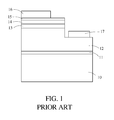
As shown in FIG. 1, the structure of GaN series LED includes a sapphire substrate 10, a GaN buffer layer 11, an n-type doping GaN ohmic contact layer 12, an indium gallium nitride (InGaN) light-emitting layer 13, and a p-type doping GaN layer 14. Then, through photolithography and etching processes, the n-type doping GaN ohmic contact layer 12, the InGaN light-emitting layer 13 and the p-type doping GaN layer 14 are partially removed to expose a partial surface of the n-type doping GaN ohmic contact layer 12. In addition, a transparent conductive layer 15 is formed over the p-type doping GaN layer 14; a p-type metal electrode 16 is disposed over the transparent conductive layer 15; and an n-type metal electrode 17 is disposed on the surface of the n-type doping GaN ohmic contact layer 12. Thus, the so-called conventional lateral electrode structure of the GaN series LED is formed.
Referring now to FIG. 2, the structural schematic view includes a sapphire substrate 20, a GaN buffer layer 21, an n-type doping GaN ohmic contact layer 22, an n-type doping aluminum indium gallium nitride superlattice stacked structure 23, an InGaN light-emitting layer 24, a p-type doping GaN layer 25, a transparent conductive layer 26, a p-type metal electrode 27, and an n-type metal electrode 28. Wherein, the n-type doping aluminum indium gallium nitride superlattice stacked structure 23 is composed of a number of aluminum indium gallium nitride layers with different thicknesses and composition, and the thickness difference is less than or equal to 50 Å.
Moreover, referring now to FIG. 3, it is a structural schematic view showing another GaN series LED disclosed by a prior art for improving light-emitting efficiency. The GaN series LED element includes an InGaN multiple quantum well (MQW) light-emitting layer 200 with periodic thickness variance, which is formed over an n-type doping GaN layer 100. The n-type doping GaN layer 100 is composed of an n-type doping GaN layer 100 a with a growth temperature ranging from 1000 to 1050° C., and an n-type doping GaN layer 100 b with a relative growth temperature ranging from 880 to 920° C.; the MQW light-emitting layer 200 produces periodic thickness variance because the added n-type doping GaN layer 100 b grows in low temperature, and the preferred thickness of the n-type doping GaN layer 100 b is about 1000 Å. However, the light-emitting efficiency of the conventional LED is still limited, and there is a need for further improvement.
SUMMARY OF THE INVENTION
The main object of the present invention is to provide a GaN series high light-emitting efficiency LED structure, wherein the GaN series LED structure includes an interface blocking layer to effectively reduce density of the non-radiative recombination center, and to further improve the light-emitting efficiency.
The present invention further improves the internal quantum efficiency through the n-type doping superlattice structure and the n-type doping GaN layer which block the non-radiative recombination.
In the present invention, by way of lowering temperature and adjusting the environment of the epitaxy reaction chamber, epitaxy grows in the interface blocking structure and the light-emitting layer under pure nitrogen and low temperature, so as to improve the efficiency of radiative recombination.
In addition, the present invention mainly provides a GaN series LED structure, including a substrate, at least one GaN series layer, a light-emitting layer, a p-type GaN series layer, and at least one interface blocking layer. Wherein, the GaN series layer is formed over the substrate; the light-emitting layer is formed over the GaN series layer; the p-type GaN series layer is formed over the light-emitting layer; and the interface blocking layer is formed between the GaN series layer and the light-emitting layer.
In which, the interface blocking layer is composed of an n-type GaN series superlattice structure stacked with an n-type GaN layer.
In which, the epitaxy growth temperature of the interface blocking layer ranges from 835° C. to 950° C.
In which, the thickness of the n-type GaN layer in the combination of the interface blocking layer is less than 1400 Å.
In which, the n-type GaN series superlattice structure in the combination of the interface blocking layer is composed of an aluminum indium gallium nitride layer mutually stacked with a GaN layer.
In which, the preferred range of the thickness of the n-type GaN layer is between 300 Ř1400 Å.
In which, the preferred range of the thickness of the n-type GaN series superlattice structure is between 600 Ř800 Å.
In which, the composition proportion of aluminum in the aluminum indium gallium nitride layer of the n-type GaN series superlattice structure ranges from 5% to 10%.
In which, the n-type GaN series superlattice structure further includes an InGaN layer subsequently and mutually stacked with the GaN layer.
In which, the composition proportion of indium in the InGaN layer is less than 10%, and the thickness of the InGaN layer is no more than 15 Å.
In addition, the present invention provides a GaN series LED structure, including a substrate, a GaN series buffer layer, a first n-type GaN series superlattice structure layer, a first n-type GaN series layer, a second n-type GaN series superlattice structure layer, a third n-type GaN series layer, a light-emitting layer, and a p-type GaN series layer. In which, the GaN series buffer layer is formed over the substrate; the first n-type GaN series superlattice structure layer is formed over the GaN series buffer layer; the first n-type GaN series layer is formed over the first n-type GaN series superlattice structure layer; the second n-type GaN series superlattice structure layer is formed over the first n-type GaN series layer; the third n-type GaN series layer is formed over the second n-type GaN series superlattice structure layer; the light-emitting layer is formed over the third n-type GaN series layer; and the p-type GaN series layer is formed over the light-emitting layer.
In which, an interface blocking layer is composed of the second n-type GaN series superlattice structure stacked with the third n-type GaN layer.
In which, the p-type GaN series layer is composed of a p-type cladding layer and a p-type ohmic contact layer.
In which, the p-type cladding layer is a superlattice structure composed of a p-type GaN series layer.
BRIEF DESCRIPTION OF THE DRAWINGS
FIG. 1 is a schematic view of a LED structure in prior art;
FIG. 2 is a schematic view of another LED structure in prior art;
FIG. 3 is a schematic view of another LED structure in prior art;
FIG. 4 is a structural schematic view of a preferred reference case of the LED, according to the present invention;
FIG. 5 is a structural schematic view of an embodiment of the LED according to the present invention;
FIG. 6 is a structural schematic view of another embodiment of the LED according to the present invention;
FIG. 7 is a structural schematic view of a preferred embodiment of the LED according to the present invention;
FIG. 8 is an EL intensity trend comparison view of the preferred embodiments according to the present invention; and
FIG. 9 is a light-emitting layer TEM view of a preferred embodiment according to the present invention.
DETAILED DESCRIPTION OF THE INVENTION
Referring now to FIGS. 4 to 9, the present invention provides a GaN series LED structure. First, referring to FIG. 4, it is a cross-section schematic view of a preferred reference case of the LED structure according to the present invention. The LED structure is mainly composed of a substrate 40, a low temperature GaN buffer layer 41, a non-doped type high temperature GaN layer 42, an n-type doping high temperature GaN ohmic contact layer 43, a light-emitting layer 44, a p-type doping aluminum gallium nitride cladding layer 45, and a p-type doping GaN ohmic contact layer 46. In which, the material of the substrate 40 is chosen from one of the following, including sapphire, carborundum, zinc oxide, zirconium diboride, spinel, lithium galliate, lithium aluminate, gallium trioxide, or silicon materials. First, after a low temperature GaN buffer layer 41 with a thickness of about 250 Å and a non-doped type high temperature GaN layer 42 with a thickness of about 1.2 μm are formed over the substrate 40 through the MOCVD method, epitaxy sequentially forms the GaN ohmic contact layer 43 over the GaN layer 42. Wherein, the n-type carrier doping concentration and growth thickness of the GaN ohmic contact layer 43 are about 4×10+18 cm−3 and 4 μm, respectively. Then, the MQW light-emitting layer 44 is composed of an InGaN quantum well without carrier doping and with a thickness of about 25 Å, and a GaN barrier layer with a thickness of about 125 Å. After the growth of the epitaxy of the light-emitting layer 44 is achieved, a cladding layer 45 composed of aluminum gallium nitride with a thickness of about 400 Å and a p-type carrier doping concentration of about 8×10+19 cm−3, and a p-type GaN ohmic contact layer 46 with a thickness of about 2500 Å and carrier doping concentration of about 1×10+20 cm−3 are grown. After the growth of epitaxy of the whole LED is achieved, a partial surface of the n-type GaN ohmic contact layer, a portion of the light-emitting layer, and a portion of the p-type aluminum gallium nitride cladding layer and the GaN ohmic contact layer are etched and removed through the conventional lateral electrode dice process method. A transparent conductive layer 47 is deposited over the p-type GaN ohmic contact layer, and a p-type metal electrode 48 and an n-type metal electrode 49 are made. After the dice process is finished, the substrate 40 is ground to have a thickness of about 90 um, and is made as an LED dice with a dimension of 325 um×325 um through the conventional laser cutting process and splitting methods. After the LED dice process is finished, the dice is fixed on the TO-can, and the p-type and n-type metal electrodes are connected with the electrodes on the TO-can by golden threads, then the dice is put into an integrating sphere to be driven by DC 20 mA, so as to get an EL intensity of about 4.5×10⁻⁷, which is equivalent to an output power of about 4.2 mW.
Referring now to FIG. 5, a cross-section schematic view of a preferred embodiment of the LED structure is shown according to the present invention. The LED structure is mainly composed of a substrate 50, a low temperature GaN buffer layer 51, a non-doped type high temperature GaN layer 52, a superlattice structure layer 53 composed of an n-type doping high temperature GaN and aluminum gallium nitride, an n-type doping GaN ohmic contact layer 54, an n-type doping GaN and aluminum gallium nitride superlattice structure layer 55, a light-emitting layer 56, a p-type doping aluminum gallium nitride cladding layer 57, a p-type doping GaN ohmic contact layer 58, a transparent conductive layer 59, a p-type metal electrode 60, and an n-type metal electrode 61. First, after the low temperature GaN buffer layer 51 with a thickness of about 250 Å and the non-doped type high temperature GaN layer 52 with a thickness of about 1.2 μm are formed over the substrate 50 through the MOCVD method, epitaxy sequentially forms the superlattice structure layer 53 over the GaN layer 52, wherein the superlattice structure layer 53 is composed of a high temperature GaN with an n-type carrier doping concentration of about 6×10+18 cm−3 and aluminum gallium nitride, then each of the above respectively with a thickness of 20 Å repeats 15 times of overtapping growth, and epitaxy forms the n-type GaN ohmic contact layer 54 over the superlattice structure layer 53, in which the growth thickness and the n-type carrier doping concentration of the n-type GaN ohmic contact layer 54 are about 4 μm and 4×10+18 cm−3, respectively. Then, epitaxy repeatedly grows a superlattice structure layer 53, which is changed to have an n-type carrier doping concentration of about 1×10+18 cm−3 to form another superlattice structure layer 55. Then, the MQW light-emitting layer 56 is composed of an InGaN quantum well without carrier doping and with a thickness of about 25 Å, and a GaN barrier layer with a thickness of about 125 Å. After the growth of the epitaxy of the light-emitting layer is achieved, the p-type aluminum gallium nitride cladding layer 57 with a carrier doping concentration of about 8×10+19 cm−3 and a thickness of about 400 Å is grown. Finally, the p-type GaN ohmic contact layer 58 with a thickness of about 2500 Å and a carrier doping concentration of about 1×10+20 cm−3 is formed. Based on the dice process method disclosed by the above preferred reference case, an LED dice with a dimension of 325 um×325 um is made, and is applied with DC 20 mA, so as to get an EL intensity of about 4.9×10⁻⁷, which is equivalent to an output power of about 4.65 mW with a 10% increase.
Referring now to FIG. 6, a cross-section schematic view of another preferred embodiment of an LED structure according to the present invention is shown. The LED structure mainly depends on the embodiment shown in FIG. 5, but adopts a p-type superlattice structure, which is composed of a p-type doping aluminum gallium nitride layer 57 a with a thickness of about 20 Å and a p-type doping GaN layer 57 b with a thickness of about 20 Å by repeating 20 times of overtapping growth, in replacement of the p-type doping aluminum gallium nitride cladding layer 57. In addition, the epitaxy growth temperature, thickness, and carrier doping concentration of the structure maintains the same. Based on the above preferred reference case, the LED dice with a dimension of 325 um×325 um is made and is applied with DC 20 mA, so as to get an EL intensity of about 5.83×10⁻⁷, which is equivalent to an output power of about 5.45 mW with a 30% increase compared with the embodiment shown in FIG. 4.
Referring now to FIG. 7, a cross-section schematic view of another preferred embodiment of an LED structure according to the present invention is illustrated. The LED structure mainly depends on the embodiment shown in FIG. 6, but a modification of another preferred embodiment of the present invention. According to prior art, in general, if the GaN series LED structure is grown by the MOCVD method, the so-called high temperature growth layer means that the temperature of the growth reaction chamber ranges from 980 to 1050° C.; when the InGaN light-emitting layer structure is grown, the growth temperature of the reaction chamber must be reduced to a range of 700 to 835° C. to control the indium atoms combination in the light-emitting layer for obtaining the LED element emitting in blue-green wavelength range. In view of this, if the temperature of the growth reaction chamber is reduced from 980˜1050° C. to 700˜835° C., the growth interface following the InGaN light-emitting layer will produce additional vacancy bonding, which is not conductive to the follow-up growth of the InGaN light-emitting layer with high quality. Therefore, the embodiment adopts an interface blocking layer to separate the defect produced by the vacancy bonding, so as to get the preferred InGaN/GaN MQW light-emitting layer. The preferred implementation is described as follows:
After a low temperature GaN buffer layer 71 with a thickness of about 250 Å and a non-doped type high temperature GaN layer 72 with a thickness of about 1.2 μm are formed over a substrate 70, epitaxy sequentially forms a superlattice structure layer 73 over the GaN layer 72, wherein the superlattice structure layer 73 is composed of high temperature GaN with an n-type carrier doping concentration of about 6×10+18 cm−3 and aluminum gallium nitride, then each of the above respectively with a thickness of 20 Å repeats 15 times of overtapping growth, and epitaxy forms an n-type GaN ohmic contact layer 74 over the superlattice structure layer 73, in which the growth thickness and the n-type carrier doping concentration of the n-type GaN ohmic contact layer 74 are about 4 μm and 4×10+18 cm−3, respectively. Then, the temperature of the growth reaction chamber is reduced from 1030° C. to 835° C., and the preferred range is between 835° C. to 950° C. During the period of lowering the temperature, hydrogen flow is reduced and nitrogen flow is increased at the same time until epitaxy growth environment is completely changed to pure nitrogen; after the flow, pressure, and temperature of the reaction chamber are stable, the epitaxy conditions of the superlattice structure layer 73 are sequentially repeated, but the n-type carrier doping concentration is changed to 1×10+18 cm−3 to form another superlattice structure layer 75. Then, another n-type doping GaN layer 300 with a different thickness is added to form the so-called interface blocking layer 400, and then an MQW light-emitting layer 76 is composed of an InGaN quantum well without carrier doping and with a thickness of about 25 Å, and a GaN barrier layer with a thickness of about 125 Å. After the growth of the epitaxy of the light-emitting layer is achieved, the epitaxy conditions of the remaining structure maintain the same as shown in FIG. 6. Based on the dice process method disclosed by the above preferred reference case, an LED dice with a dimension of 325 um×325 um is made. The experimental results of the n-type doping GaN layer 300 with a different thickness are shown in FIG. 8. When the thickness is about 700 Å and is applied with DC 20 mA, an EL intensity of about 7.1×10⁻⁷ is obtained, which is equivalent to an output power of about 6.64 mW with a 20% increase compared with the embodiment shown in FIG. 6.
Referring now to FIG. 9, a cross-section TEM view of MQW light-emitting layer according to the present invention is shown. Because there is no characteristic of thickness periodic change in the present invention, which is different with prior art, and has an inventive step.

Claims (14)

What is claimed is:
1. A GaN series LED structure, including:
a substrate;
at least one GaN series layer, wherein the GaN series layer is formed over said substrate;
a light-emitting layer, wherein the light-emitting layer is formed over said GaN series layer;
a p-type GaN series layer, wherein the p-type GaN series layer is formed over said light-emitting layer; and
at least one interface blocking layer, wherein the interface blocking layer is formed between said GaN series layer and said light-emitting layer.
2. The GaN series LED structure as claimed in claim 1, wherein the interface blocking layer is composed of an n-type GaN series superlattice structure stacked with an n-type GaN layer.
3. The GaN series LED structure as claimed in claim 2, wherein a thickness of the n-type GaN layer combined in the interface blocking layer is less than 1400 Å.
4. The GaN series LED structure as claimed in claim 3, wherein a range of the thickness of the n-type GaN layer is between 300 Ř1400 Å.
5. The GaN series LED structure as claimed in claim 2, wherein the n-type GaN series superlattice structure combined in the interface blocking layer is composed of a aluminum indium gallium nitride layer mutually stacked with a GaN layer.
6. The GaN series LED structure as claimed in claim 5, wherein a range of the thickness of the n-type GaN series superlattice structure is between 600 Ř800 Å.
7. The GaN series LED structure as claimed in claim 5, wherein a composition proportion of aluminum in the aluminum indium gallium nitride layer of the n-type GaN series superlattice structure is between 5%˜10%.
8. The GaN series LED structure as claimed in claim 2, wherein the n-type GaN series superlattice structure further includes an InGaN layer subsequently and mutually stacked with the GaN layer.
9. The GaN series LED structure as claimed in claim 8, wherein a composition proportion of indium in the InGaN layer is less than 10%, and a thickness of the InGaN layer is no more than 15 Å.
10. The GaN series LED structure as claimed in claim 1, wherein an epitaxy growth temperature of the interface blocking layer ranges from 835° C. to 950° C.
11. A GaN series LED structure, including:
a substrate;
a GaN series buffer layer, wherein the GaN series buffer layer is formed over said substrate;
a first n-type GaN series superlattice structure layer, wherein the first n-type GaN series superlattice structure layer is formed over the GaN series buffer layer;
a first n-type GaN series layer, wherein the first n-type GaN series layer is formed over said first n-type GaN series superlattice structure layer;
a second n-type GaN series superlattice structure layer, wherein the second n-type GaN series superlattice structure layer is formed over said first n-type GaN series layer;
a third n-type GaN series layer, wherein the third n-type GaN series layer is formed over said second n-type GaN series superlattice structure layer;
a light-emitting layer, wherein the light-emitting layer is formed over said third n-type GaN series layer; and
a p-type GaN series layer, wherein the p-type GaN series layer is formed over said light-emitting layer.
12. The GaN series LED structure as claimed in claim 11, wherein an interface blocking layer is composed of said second n-type GaN series superlattice structure stacked with said third n-type GaN layer.
13. The GaN series LED structure as claimed in claim 11, wherein the p-type GaN series layer is composed of a p-type cladding layer and a p-type ohmic contact layer.
14. The GaN series LED structure as claimed in claim 13, wherein the p-type cladding layer is a superlattice structure composed of a p-type GaN series layer.
US12/694,600 2010-01-27 2010-01-27 GaN series light-emitting diode structure Expired - Fee Related US8138494B2 (en)

Priority Applications (1)

Application Number Priority Date Filing Date Title
US12/694,600 US8138494B2 (en) 2010-01-27 2010-01-27 GaN series light-emitting diode structure

Applications Claiming Priority (1)

Application Number Priority Date Filing Date Title
US12/694,600 US8138494B2 (en) 2010-01-27 2010-01-27 GaN series light-emitting diode structure

Publications (2)

Publication Number Publication Date
US20110180778A1 US20110180778A1 (en) 2011-07-28
US8138494B2 true US8138494B2 (en) 2012-03-20

Family

ID=44308284

Family Applications (1)

Application Number Title Priority Date Filing Date
US12/694,600 Expired - Fee Related US8138494B2 (en) 2010-01-27 2010-01-27 GaN series light-emitting diode structure

Country Status (1)

Country Link
US (1) US8138494B2 (en)

Families Citing this family (9)

* Cited by examiner, † Cited by third party
Publication number Priority date Publication date Assignee Title
JP2010087217A (en) * 2008-09-30 2010-04-15 Toyoda Gosei Co Ltd Group-iii nitride semiconductor light-emitting element, and method of manufacturing the same
CN102280542B (en) * 2011-09-02 2013-03-27 华灿光电股份有限公司 Method for growing GaN-based light emitting diode multiquantum well
CN103165769B (en) * 2013-02-28 2015-05-13 溧阳市宏达电机有限公司 Manufacture method of light emitting diode (LED)
CN106537617B (en) 2014-05-27 2019-04-16 斯兰纳Uv科技有限公司 Use the advanced electronics structure of semiconductor structure and superlattices
KR102439708B1 (en) 2014-05-27 2022-09-02 실라나 유브이 테크놀로지스 피티이 리미티드 An optoelectronic device
WO2015181656A1 (en) * 2014-05-27 2015-12-03 The Silanna Group Pty Limited Electronic devices comprising n-type and p-type superlattices
US11322643B2 (en) 2014-05-27 2022-05-03 Silanna UV Technologies Pte Ltd Optoelectronic device
CN105679907B (en) * 2016-03-04 2018-06-26 华灿光电股份有限公司 High brightness LED epitaxial wafer and preparation method thereof
US10121932B1 (en) * 2016-11-30 2018-11-06 The United States Of America As Represented By The Secretary Of The Navy Tunable graphene light-emitting device

Citations (1)

* Cited by examiner, † Cited by third party
Publication number Priority date Publication date Assignee Title
US20110303891A1 (en) * 2006-09-06 2011-12-15 Palo Alto Research Center Incorporated Mixed Alloy Defect Redirection Region and Devices Including Same

Patent Citations (1)

* Cited by examiner, † Cited by third party
Publication number Priority date Publication date Assignee Title
US20110303891A1 (en) * 2006-09-06 2011-12-15 Palo Alto Research Center Incorporated Mixed Alloy Defect Redirection Region and Devices Including Same

Also Published As

Publication number Publication date
US20110180778A1 (en) 2011-07-28

Similar Documents

Publication Publication Date Title
US8138494B2 (en) GaN series light-emitting diode structure
US10700237B2 (en) Ultraviolet light-emitting devices incorporating graded layers and compositional offsets
JP6589987B2 (en) Nitride semiconductor light emitting device
TWI603500B (en) Nitride semiconductor light-emitting device
US8314415B2 (en) Radiation-emitting semiconductor body
KR100541102B1 (en) Nitride semiconductor light emitting diode and fabrication method thereof
JP5050574B2 (en) Group III nitride semiconductor light emitting device
US8304756B2 (en) Deep ultraviolet light emitting device and method for fabricating same
KR100482511B1 (en) Ⅲ-Nitride compound semiconductor light emitting device
WO2010100844A1 (en) Nitride semiconductor element and method for manufacturing same
CN109075226B (en) Group III nitride laminate and group III nitride light-emitting element
TWI684291B (en) Nitride semiconductor ultraviolet light emitting element
JP2010539731A (en) (Al, In, Ga, B) N device on patterned substrate
JP2023510977A (en) Red LED and manufacturing method
JP2008182069A (en) Semiconductor light-emitting element
JP2010010678A (en) Quantum dot device and method of manufacturing the same
TW201015751A (en) Polychromatic wavelengths LED and manufacturing method thereof
JP2001203385A (en) Nitride semiconductor light emitting diode
JP2023536361A (en) LED device and method for manufacturing LED device
JP2006339426A (en) Light-emitting diode and its fabrication method
KR20130022815A (en) Nitride semiconductor light emitting device and manufacturing method thereof
KR20050096010A (en) Nitride semiconductor light emitting diode and fabrication method thereof
TW201528441A (en) Manufacturing method of nitride semiconductor component
KR20130055976A (en) Light emitting diode having void layer and method of fabricating the same
TWI396306B (en) Gallium nitride based light emitting diode structure and its making method

Legal Events

Date Code Title Description
AS Assignment

Owner name: CHANG GUNG UNIVERSITY, TAIWAN

Free format text: ASSIGNMENT OF ASSIGNORS INTEREST;ASSIGNORS:LIN, RAY-MING;JIANG, JHONG-HAO;FANG, BOR-REN;REEL/FRAME:023857/0524

Effective date: 20100127

STCF Information on status: patent grant

Free format text: PATENTED CASE

FPAY Fee payment

Year of fee payment: 4

FEPP Fee payment procedure

Free format text: MAINTENANCE FEE REMINDER MAILED (ORIGINAL EVENT CODE: REM.); ENTITY STATUS OF PATENT OWNER: SMALL ENTITY

LAPS Lapse for failure to pay maintenance fees

Free format text: PATENT EXPIRED FOR FAILURE TO PAY MAINTENANCE FEES (ORIGINAL EVENT CODE: EXP.); ENTITY STATUS OF PATENT OWNER: SMALL ENTITY

STCH Information on status: patent discontinuation

Free format text: PATENT EXPIRED DUE TO NONPAYMENT OF MAINTENANCE FEES UNDER 37 CFR 1.362

FP Lapsed due to failure to pay maintenance fee

Effective date: 20200320