US8099685B2 - Model based microdevice design layout correction - Google Patents
Model based microdevice design layout correction Download PDFInfo
- Publication number
- US8099685B2 US8099685B2 US12/184,089 US18408908A US8099685B2 US 8099685 B2 US8099685 B2 US 8099685B2 US 18408908 A US18408908 A US 18408908A US 8099685 B2 US8099685 B2 US 8099685B2
- Authority
- US
- United States
- Prior art keywords
- adjustment
- shapes
- selecting
- subset
- shape
- Prior art date
- Legal status (The legal status is an assumption and is not a legal conclusion. Google has not performed a legal analysis and makes no representation as to the accuracy of the status listed.)
- Active, expires
Links
Images


Classifications
-
- G—PHYSICS
- G06—COMPUTING; CALCULATING OR COUNTING
- G06F—ELECTRIC DIGITAL DATA PROCESSING
- G06F30/00—Computer-aided design [CAD]
- G06F30/30—Circuit design
- G06F30/39—Circuit design at the physical level
- G06F30/398—Design verification or optimisation, e.g. using design rule check [DRC], layout versus schematics [LVS] or finite element methods [FEM]
-
- G—PHYSICS
- G06—COMPUTING; CALCULATING OR COUNTING
- G06F—ELECTRIC DIGITAL DATA PROCESSING
- G06F2119/00—Details relating to the type or aim of the analysis or the optimisation
- G06F2119/18—Manufacturability analysis or optimisation for manufacturability
-
- Y—GENERAL TAGGING OF NEW TECHNOLOGICAL DEVELOPMENTS; GENERAL TAGGING OF CROSS-SECTIONAL TECHNOLOGIES SPANNING OVER SEVERAL SECTIONS OF THE IPC; TECHNICAL SUBJECTS COVERED BY FORMER USPC CROSS-REFERENCE ART COLLECTIONS [XRACs] AND DIGESTS
- Y02—TECHNOLOGIES OR APPLICATIONS FOR MITIGATION OR ADAPTATION AGAINST CLIMATE CHANGE
- Y02P—CLIMATE CHANGE MITIGATION TECHNOLOGIES IN THE PRODUCTION OR PROCESSING OF GOODS
- Y02P90/00—Enabling technologies with a potential contribution to greenhouse gas [GHG] emissions mitigation
- Y02P90/02—Total factory control, e.g. smart factories, flexible manufacturing systems [FMS] or integrated manufacturing systems [IMS]
Definitions
- the invention relates to the field of circuit design layout correction. More specifically, various embodiments of the invention relate to employing models to evaluate and propose adjustments to a circuit design layout.
- Designing and fabricating microcircuit devices typically involves many steps, sometimes referred to as the “design flow.” The particular steps of a design flow often are dependent upon the type of microcircuit, its complexity, the design team, and the microcircuit fabricator or foundry that will manufacture the microcircuit.
- software and hardware “tools” verify the design at various stages of the design flow by running software simulators and/or hardware emulators, these steps aid in the discovery of errors in the design and allow the designers and engineers to correct or otherwise improve the design.
- HDL Hardware Design Language
- VHDL Very high speed integrated circuit Hardware Design Language
- the device design which is typically in the form of a schematic or netlist, describes the specific electronic devices (such as transistors, resistors, and capacitors) that will be used in the circuit, along with their interconnections.
- This device design generally corresponds to the level of representation displayed in conventional circuit diagrams.
- the relationships between the electronic devices are analyzed, to confirm that the circuit described by the device design will correctly perform the desired functions. This analysis is sometimes referred to as “formal verification.” Additionally, preliminary timing estimates for portions of the circuit are often made at this stage, using an assumed characteristic speed for each device, and incorporated into the verification process.
- the design is again transformed, this time into a physical design that describes specific geometric elements.
- This type of design often is referred to as a “layout” design.
- the geometric elements which typically are polygons, define the shapes that will be created in various materials to manufacture the circuit.
- a designer will select groups of geometric elements representing circuit device components (e.g., contacts, gates, etc.) and place them in a design area. These groups of geometric elements may be custom designed, selected from a library of previously-created designs, or some combination of both. Lines are then routed between the geometric elements, which will form the wiring used to interconnect the electronic devices.
- Layout tools (often referred to as “place and route” tools), such as Mentor Graphics' IC Station or Cadence's Virtuoso, are commonly used for both of these tasks.
- the Graphic Data System II (GDSII) format is a popular format for transferring and archiving 2D graphical IC layout data. Among other features, it contains a hierarchy of structures, each structure containing layout elements (e.g., polygons, paths or poly-lines, circles and textboxes).
- Other formats include an open source format named Open Access, Milkyway by Synopsys, Inc., EDDM by Mentor Graphics, Inc., and the more recent Open Artwork System Interchange Standard (OASIS) proposed by Semiconductor Equipment and Materials International (SEMI). These various industry formats are used to define the geometrical information in IC layout designs that are employed to manufacture integrated circuits. Once the microcircuit device design is finalized, the layout portion of the design can be used by fabrication tools to manufacturer the device using a photolithographic process.
- OASIS Open Artwork System Interchange Standard
- Each mask is created from circuit layout data. That is, the geometric elements described in layout design data define the relative locations or areas of the circuit device that will be exposed to radiation through the mask.
- a mask or reticle writing tool is used to create the mask or reticle based upon the layout design data, after which the mask can be used in a photolithographic process.
- a layout design is made up of a variety of geometric elements.
- the edges of the geometric elements (which are typically polygons) are fragmented, and the edge fragments are rearranged or edited to effect the desired modifications.
- the edge fragments are typically reconfigured to ensure the design conforms to manufacturing constraints, such as the minimum size of a fragment or the minimum proximity between adjacent fragments.
- features that will increase the fidelity of the photolithographic process are often added to the design. For example, some optical proximity correction processes will reconfigure the edge fragments of a polygon to create serifs at one or more corners.
- any manufacturing defect whether due to the lithographic process or some other process such as chemical-mechanical planarization will be referred to herein as a “fault,” a “potential fault,” or a “potential manufacturing fault.”
- aspects of the invention relate to techniques for evaluating microdevice design layout data and determining adjustments that, if implemented in the layout design, may reduce or correct potential manufacturing faults.
- Various implementations of the invention provide methods for compiling a set of potential adjustments or corrections to microdevice design layout data.
- features nearby a potential fault are extracted.
- a model is used to determine the contribution of these neighboring features to the potential fault. Adjustments then are made to the neighboring features, and the effect of these adjustments upon the potential fault are evaluated using the model.
- the potential adjustments to the microdevice design layout data are ranked.
- the techniques are used on multiple potential faults within the microdevice design layout design. Additionally, in some implementations, these techniques are used in addition to or in conjunction with other fault correction procedures, such as optical proximity correction.
- FIG. 1 illustrates an example computing device
- FIG. 2 is illustrative of a graphical representation of an example microdevice design layout
- FIG. 3 illustrates a flow chart describing an implementation of various embodiments of the present invention
- FIG. 5 is illustrative of a graphical representation of an example microdevice design layout
- FIG. 6 illustrates a flow chart describing an implementation of various embodiments of the present invention
- FIG. 9 illustrates the results of an implementation of various embodiments of the present invention applied to the example microdevice design layout of FIG. 2 .
- FIG. 10 illustrates the example microdevice design layout of FIG. 2 , highlighting possible adjustments to the shapes
- FIG. 12 illustrates the example microdevice design layout of FIG. 2 with a possible adjustment to the shapes implemented
- FIG. 13 illustrates the example microdevice design layout of FIG. 2 with a possible adjustment to the shapes implemented
- FIG. 14 illustrates the example microdevice design layout of FIG. 2 with a possible adjustment to the shapes implemented
- the disclosed technology includes all novel and unobvious features, aspects, and embodiments of the system and methods described herein both alone, and in various combinations and sub-combinations thereof.
- the disclosed features, aspects, and embodiments can be used alone or in various novel and unobvious combinations and sub-combinations with one another.
- Some of the methods described herein can be implemented in software stored on a computer-readable medium and executed on a computer. Some of the disclosed methods, for example, can be implemented as part of a computer-implemented electronic design automation (EDA) tool. Such methods can be executed on a single computer or a networked computer. For clarity, only those aspects of the software germane to these disclosed methods are described; product details well known in the art are omitted.
- EDA electronic design automation
- FIG. 1 shows an illustrative example of a computing device 101 .
- the computing device 101 includes a computing unit 103 with a processing unit 105 and a system memory 107 .
- the processing unit 105 may be any type of programmable electronic device for executing software instructions, but will conventionally be a microprocessor or a combination of two or more microprocessors.
- the system memory 107 may include both a read-only memory (ROM) 109 and a random access memory (RAM) 111 .
- ROM read-only memory
- RAM random access memory
- both the read-only memory (ROM) 109 and the random access memory (RAM) 111 may store software instructions for execution by the processing unit 105 .
- the processing unit 105 and the system memory 107 are connected, either directly or indirectly, through a bus 113 or alternate communication structure, to one or more peripheral devices.
- the processing unit 105 or the system memory 107 may be directly or indirectly connected to one or more additional memory storage devices, such as a “hard” magnetic disk drive 115 , a removable magnetic disk drive 117 , an optical disk drive 119 , or a flash memory card 121 .
- the processing unit 105 and the system memory 107 also may be directly or indirectly connected to one or more input devices 123 and one or more output devices 125 .
- the input devices 123 may include, for example, a keyboard, a pointing device (such as a mouse, touchpad, stylus, trackball, or joystick), a scanner, a camera, and a microphone.
- the output devices 125 may include, for example, a monitor display, a printer and speakers.
- one or more of the peripheral devices 115 - 125 may be internally housed with the computing unit 103 .
- one or more of the peripheral devices 115 - 125 may be external to the housing for the computing unit 103 and connected to the bus 113 through, for example, a Universal Serial Bus (USB) connection.
- USB Universal Serial Bus
- the computing unit 103 may be directly or indirectly connected to one or more network interfaces 127 for communicating with other devices making up a network.
- the network interface 127 translates data and control signals from the computing unit 103 into network messages according to one or more communication protocols, such as the transmission control protocol (TCP) and the Internet protocol (IP).
- TCP transmission control protocol
- IP Internet protocol
- the interface 127 may employ any suitable connection agent (or combination of agents) for connecting to a network, including, for example, a wireless transceiver, a modem, or an Ethernet connection.
- TCP transmission control protocol
- IP Internet protocol
- connection agent or combination of agents
- the computer 101 is illustrated as an example only, and is not intended to be limiting.
- Various embodiments of the invention may be implemented using one or more computing devices that include the components of the computer 101 illustrated in FIG. 1 , which include only a subset of the components illustrated in FIG. 1 , or which include an alternate combination of components, including components that are not shown in FIG. 1 .
- various embodiments of the invention may be implemented using a multi-processor computer, a plurality of single and/or multiprocessor computers arranged into a network, or some combination of both.
- microdevice design layout data is generally preprocessed to ensure that the layout both complies with the design specification and that the layout will be manufactured without any faults.
- techniques available to designers for example optical proximity correction, which processes the geometric elements, or polygons in the microdevice design layout and adjusts them according to specified process parameters.
- performing these techniques is time consuming and computationally expensive. Accordingly, various methods and systems are disclosed herein that provide for analyzing a microdevice design layout and employing a model-based methodology to compile a set of possible adjustments to the microdevice design layout.
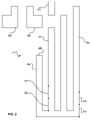
- FIG. 2 illustrates an example of a portion of a microdevice design layout 201
- microdevice design layout data although stored in electronic format, is often discussed or represented in graphical format as illustrated by the microdevice design layout 201 of FIG. 2 .
- the graphical representation of microdevice design layout data is facilitated by representing the features as polygons.
- the polygons are composed of edges and edge fragments.
- the microdevice design layout 201 of FIG. 2 contains a potential manufacturing fault 203 and edges 205 .
- the edges 205 combine to form polygons 207 .
- the edges 205 are often fractured to form edge fragments 209 .
- microdevice design layout 201 are used by microdevice design layout data processing tools. More particularly, the edges 205 , the edge fragments 209 , and the polygons 207 are often used by these processing tools to detect and correct potential manufacturing faults.
- edge fragments may vary from implementation to implementation. Accordingly, the size and location of edge fragments within a particular microdevice design layout will vary depending upon the particular implementations, possible user input, design constraints, or manufacturing constraints.
- FIG. 3 illustrates an example of a model-based layout correction assessment process 301 that may be implemented according to various embodiments of the present invention.
- the correction assessment process 301 may be used to process a portion of a microdevice design layout 303 .
- the correction assessment process 301 could be used to process the microdevice design layout 201 of FIG. 2 .
- the correction assessment process 301 includes a step for extracting shapes S 305 , a step for identifying aggressor shapes S 307 , and a step for simulating possible adjustments to the shapes S 309 .
- the model-based layout correction assessment process 301 produces a set of possible adjustments 311 , which may be applied to the microdevice design layout 303 .
- the microdevice design layout 303 contains a potential manufacturing fault.
- the microdevice design layout 201 of FIG. 2 contains the potential manufacturing fault 203 , which is a pinching type fault.
- the step for extracting shapes S 305 identifies a plurality of shapes neighboring the potential manufacturing fault.
- the step for extracting shapes S 305 identifies entire polygons and associates the identified polygons as the shapes neighboring the potential fault.
- the step for extracting shapes S 305 identifies edges and associates the identified edges as the shapes neighboring the potential fault.
- the step for extracting shapes S 305 identifies edge fragments and associates the identified edge fragments as the shapes neighboring the potential fault.
- a vector is used to store the identified shapes, as illustrated by Equation 1. e 0 e 1 e 2 . . . e n 1
- the model-based layout correction assessment process 301 may be utilized to process the microdevice design layout 201 .
- the step for extracting shapes S 305 identifies the polygons 207 near the potential manufacturing fault 203 .
- the step for extracting shapes S 305 identifies the edges 205 near the potential manufacturing fault 203 .
- the step for extracting shapes S 305 identifies the edge fragments 209 near the potential manufacturing fault 203 .
- the vector represented by Equation 1 is utilized to store the locations of the extracted shapes, be the extracted shapes, edges, polygons, or edge fragments.
- a model is employed in both the step for identifying aggressor shapes S 307 and the step for simulating possible adjustments to the shapes S 309 .
- the model-based layout correction assessment process 301 utilizes a pre-calibrated model. While in other embodiments of the invention, the model-based layout correction assessment process 301 calibrates the model prior to performing the step for identifying aggressor shapes S 307 and the step for simulating possible adjustments to the shapes S 309 .
- FIG. 4 illustrates an example of a model calibration flow 401 that may be implemented according to various embodiments of the present invention.
- the model calibration flow includes a step for measuring the layout S 403 , a step for performing regression analysis S 405 , and a step for performing model fitting S 407 .
- the densities are measured by superimposing a grid over the potential manufacturing fault.
- FIG. 5 illustrates a microdevice design layout 501 , including a target polygon 503 , neighbor polygons 505 , and density kernels 507 .
- the target polygon 503 contains a potential manufacturing fault 509 .
- a density measurement is taken for each of the density kernels 507 .
- the density measurement is the difference between the edge of the target polygon 503 and the center of the density kernel 507 .
- a vector of densities is formed, as shown in Equation 2. [1d 1 d 2 . . . d j] 2
- the step for measuring the layout S 403 measures the contour and densities of a representative layout of the microdevice design layout data 303 .
- the contours are approximated using a Manhattan distance approximation. While with other embodiments of the invention, the contours are approximated by their orthogonal convexity. Additionally, with various embodiments of the invention, a vector of contour coefficients is formed, as shown in Equation 3.
- the step for performing regression analysis S 405 is completed by way of a linear regression method.
- a linear regression method For example, a single value decomposition (SVD) least squares method.
- SVD single value decomposition
- Equation 4 illustrates a model in the form of a Taylor series expansion, which may be used to model the microdevice design layout 303 .
- the model is a polynomial.
- Equation 5 illustrates a model in the form of a polynomial, which may be used to model the microdevice design layout 303 .
- the models described by Equations 4, 5, 6, and 7 are used during the step for identifying aggressor shapes S 307 and the step for simulating possible adjustments to the shapes S 309 . Accordingly, those of skill in the art will appreciate that the model incorporates the density measurements and the contour approximations of the microdevice design layout. For example, those represented by Equations 2 and 3.
- the size of the grid illustrated in FIG. 5 may vary for different implementations of the invention, or even within the same implementations of the invention. Additionally, those of skill in the art will appreciate that the size of the grid will affect the accuracy of the model as well as the utility of the model-based layout correction assessment process 301 . A window of 5 to 25 microns in size is suitable for some applications, while a window of 30 to 50 microns in size is suitable for other applications. The microdevice design layout and the technology underlying the design itself as well as the manufacturing process dictate the preferred window size.
- the step for determining a contour density S 603 is performed by multiplying the vectors in Equation 3 by the vector in Equation 2, as shown in Equation 8.
- the density and contour measurements used during the step for identifying aggressor shapes S 307 may be determined during the step for identifying aggressor shapes S 307 .
- a method separate from the model calibration flow 401 and the step for identifying aggressor shapes S 307 is used to determine the density and contour measurements.
- the step for determining the contour sensitivity S 605 is performed by measuring how the contour density changes with respect to the shapes extracted during the step for extracting shapes S 305 . For example, measuring how the contour density changes with respect to the edges, as illustrated by Equation 9.
- Equation 9 illustrates measuring the gradient of the density measurements and contour approximations with respect to the extracted shapes.
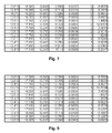
- FIG. 7 illustrates the results of an implementation of various embodiments of the present invention applied to an example microdevice design layout.
- Each row represents a different edge.
- Columns 1, 2, 3, and 4 identifying the respective edges coordinates
- column 5 identifying the gradient of the contour density with respect to the edge
- column six and column seven identify the direction and distance of a possible adjustment to the respective edges.
- the direction and distance of a possible adjustment to the respective edges is determined in the step for simulating possible adjustments to the shapes S 309 .
- FIG. 3 illustrates a model-based layout correction assessment process 301 , which may be implemented according to various embodiments of the present invention.
- the model-based layout correction assessment process 301 provides a step for simulating possible adjustments to the shapes S 309 .
- FIG. 8 illustrates a possible adjustment simulation flow 801 that may be implemented according to various embodiments of the present invention.
- the possible adjustment simulation flow 801 includes a step for selecting an edge S 803 , a step for selecting a possible adjustment to the edge S 805 , a step for simulating the affect of the possible adjustment to the edge S 807 , and a decision step S 809 .
- the step for selecting an edge S 803 is performed by selecting the edge with the largest gradient of Equation 9 first.
- the edge is selected randomly.
- the edge is selected based upon location of the edge related to the potential manufacturing fault.
- the step for selecting a possible adjustment to the edge S 805 is selected based upon the gradient of Equation 9.
- the possible edge adjustment is selected based upon user input.
- the possible edge adjustment is selected from a range. The range may be specified by the user or dictated by the underlying microdevice design layout technology and manufacturing process.
- the step for simulating the affect of the possible adjustment to the edge S 807 is performed by utilizing the chosen model to determine the amount of change necessary to resolve the potential manufacturing defect.
- multiple edge movements are simulated. More particularly, possible adjustments for multiple edges are simulated. Alternatively, multiple possible adjustments for a single edge or multiple edges may be simulated.
- the possible adjustments are made to edge fragments. Still, with other implementations of the invention the possible adjustments are made to the entire polygon.
- the possible adjustments are ranked and provided as “hints” to the user.
- the hints may be stored in vector format as illustrated in FIGS. 7 and 9 , or the hints may be formatted into a structure suitable for viewing geometric results.
- RDB Relational Database Format
- FIG. 9 illustrates the results of an implementation of various embodiments of the present invention to the example microdevice design layout of FIG. 2 . Similar to FIG. 7 , columns 1, 2, 3, and 4 identify the coordinates of the respective edge represented by each row. Column 5 identifies the gradient of the contour density with respect to the edge. Column six and column seven identify the direction and distance of a possible adjustment to the respective edges, or a “hint” to resolve the potential manufacturing fault 203 .
- FIG. 10 illustrates the microdevice design layout 201 of FIG. 2 .
- the microdevice design layout 201 illustrated in FIG. 10 includes the potential manufacturing fault 203 , as well as hints 803 , 805 , 807 , and 809 .
- FIG. 11 illustrates a microdevice design layout 1001 , derived from the microdevice design layout 201 of FIG. 2 with the hint 803 applied to the microdevice design layout 201 .
- FIG. 12 illustrates a microdevice design layout 1101 , derived from the microdevice design layout 201 of FIG. 2 with the hint 805 applied to the microdevice design layout 201 .
- FIG. 13 illustrates a microdevice design layout 1201 , derived from the microdevice design layout 201 of FIG.
- FIG. 14 illustrates a microdevice design layout 1301 , derived from the microdevice design layout 201 of FIG. 2 with the hint 809 applied to the microdevice design layout 201 .
- FIGS. 10 through 14 illustrate applying various implementations of the present invention to a microdevice design layout. Furthermore FIGS. 10 through 14 illustrate selecting a set of possible adjustments to the microdevice design layout, to resolve a potential manufacturing fault.
Landscapes
- Engineering & Computer Science (AREA)
- Computer Hardware Design (AREA)
- Physics & Mathematics (AREA)
- Theoretical Computer Science (AREA)
- Evolutionary Computation (AREA)
- Geometry (AREA)
- General Engineering & Computer Science (AREA)
- General Physics & Mathematics (AREA)
- Design And Manufacture Of Integrated Circuits (AREA)
Abstract
Description
e0e1e2 . . . en 1
[1d1d2 . . .
f=c 0 +Σc i d i 6
f=c 0 +Σc i d i +ΣΣc ij d i d j 7
d edge =l(Δe j) 10
| TABLE 1 | ||||||
| 13.615 | 16.395 | 13.615 | 17.595 | 0.0237 | 0 | 0.0676 |
| 13.415 | 16.395 | 13.415 | 17.110 | 0.1111 | 0 | 0.1446 |
| 14.015 | 16.295 | 14.015 | 17.995 | 0.0036 | 0 | 0.4475 |
| 13.815 | 16.395 | 13.815 | 17.795 | 0.0020 | 0 | 0.8153 |
| 13.615 | 17.595 | 13.515 | 17.595 | 0.0011 | 3 | 1.4408 |
| 13.515 | 17.815 | 13.515 | 18.335 | 0.0001 | 0 | 12.6474 |
| 13.415 | 17.795 | 13.215 | 17.795 | −0.0006 | 2 | 2.5876 |
| 13.815 | 17.795 | 13.715 | 17.795 | −0.0008 | 2 | 2.1016 |
| 13.215 | 17.795 | 13.215 | 17.995 | −0.0009 | 1 | 1.8240 |
| 13.615 | 17.815 | 13.515 | 17.815 | −0.0026 | 2 | 0.6264 |
| 13.415 | 17.615 | 13.415 | 17.795 | −0.0026 | 1 | 0.6230 |
| 13.115 | 17.615 | 13.415 | 17.615 | −0.0031 | 3 | 0.5161 |
| 13.415 | 17.110 | 13.315 | 17.11 | −0.0068 | 2 | 0.2347 |
| TABLE 2 | ||||||
| 13.615 | 17.595 | 13.515 | 17.595 | 0.0021 | 3 | 0.7658 |
| 13.815 | 17.595 | 13.715 | 17.795 | 0.0004 | 3 | 3.9939 |
| 13.415 | 17.795 | 13.215 | 17.795 | 0.0003 | 3 | 4.8937 |
| 13.215 | 17.795 | 13.215 | 17.995 | −0.0001 | 1 | 13.7094 |
| 14.015 | 16.295 | 14.015 | 17.995 | −0.0004 | 1 | 3.9599 |
| 13.515 | 17.815 | 13.515 | 18.335 | −0.0010 | 1 | 1.6547 |
| 13.115 | 17.615 | 13.415 | 17.615 | −0.0012 | 3 | 1.3379 |
| 13.415 | 17.110 | 13.315 | 17.110 | −0.0023 | 2 | 0.6821 |
| 13.415 | 17.615 | 13.415 | 17.795 | −0.0029 | 1 | 0.5526 |
| 13.615 | 17.815 | 13.515 | 17.815 | −0.0031 | 2 | 0.5207 |
| 13.415 | 16.395 | 13.415 | 17.110 | −0.0100 | 1 | 0.1607 |
| 13.815 | 16.395 | 13.815 | 17.795 | −0.0124 | 1 | 0.1287 |
| 13.615 | 16.395 | 13.615 | 17.595 | −0.0943 | 1 | 0.0170 |
Claims (28)
Priority Applications (2)
| Application Number | Priority Date | Filing Date | Title |
|---|---|---|---|
| US12/184,089 US8099685B2 (en) | 2007-07-31 | 2008-07-31 | Model based microdevice design layout correction |
| US12/416,077 US20100023916A1 (en) | 2007-07-31 | 2009-03-31 | Model Based Hint Generation For Lithographic Friendly Design |
Applications Claiming Priority (2)
| Application Number | Priority Date | Filing Date | Title |
|---|---|---|---|
| US96281407P | 2007-07-31 | 2007-07-31 | |
| US12/184,089 US8099685B2 (en) | 2007-07-31 | 2008-07-31 | Model based microdevice design layout correction |
Related Child Applications (1)
| Application Number | Title | Priority Date | Filing Date |
|---|---|---|---|
| US12/416,077 Continuation-In-Part US20100023916A1 (en) | 2007-07-31 | 2009-03-31 | Model Based Hint Generation For Lithographic Friendly Design |
Publications (2)
| Publication Number | Publication Date |
|---|---|
| US20090113359A1 US20090113359A1 (en) | 2009-04-30 |
| US8099685B2 true US8099685B2 (en) | 2012-01-17 |
Family
ID=40584542
Family Applications (1)
| Application Number | Title | Priority Date | Filing Date |
|---|---|---|---|
| US12/184,089 Active 2030-02-01 US8099685B2 (en) | 2007-07-31 | 2008-07-31 | Model based microdevice design layout correction |
Country Status (1)
| Country | Link |
|---|---|
| US (1) | US8099685B2 (en) |
Cited By (4)
| Publication number | Priority date | Publication date | Assignee | Title |
|---|---|---|---|---|
| US20110145772A1 (en) * | 2009-05-14 | 2011-06-16 | Pikus Fedor G | Modular Platform For Integrated Circuit Design Analysis And Verification |
| US8504954B1 (en) * | 2012-03-30 | 2013-08-06 | Apple Inc. | Methodology for automatically generating series-approximated components |
| US8549453B2 (en) * | 2012-01-31 | 2013-10-01 | Taiwan Semiconductor Manufacturing Co., Ltd. | Semiconductor device feature density gradient verification |
| US9015217B2 (en) | 2012-03-30 | 2015-04-21 | Apple Inc. | Transcendental and non-linear components using series expansion |
Families Citing this family (6)
| Publication number | Priority date | Publication date | Assignee | Title |
|---|---|---|---|---|
| US8099685B2 (en) | 2007-07-31 | 2012-01-17 | Mentor Graphics Corporation | Model based microdevice design layout correction |
| US20100023916A1 (en) * | 2007-07-31 | 2010-01-28 | Chew Marko P | Model Based Hint Generation For Lithographic Friendly Design |
| JP5309623B2 (en) * | 2008-03-10 | 2013-10-09 | 富士通セミコンダクター株式会社 | Photomask data processing method, photomask data processing system, and manufacturing method using hierarchical structure |
| US8572525B2 (en) * | 2009-08-21 | 2013-10-29 | Mentor Graphics Corporation | Partition response surface modeling |
| US8990755B2 (en) | 2011-12-29 | 2015-03-24 | Intel Corporation | Defective artifact removal in photolithography masks corrected for optical proximity |
| US9262820B2 (en) | 2014-05-19 | 2016-02-16 | United Microelectronics Corporation | Method and apparatus for integrated circuit design |
Citations (12)
| Publication number | Priority date | Publication date | Assignee | Title |
|---|---|---|---|---|
| US6430737B1 (en) * | 2000-07-10 | 2002-08-06 | Mentor Graphics Corp. | Convergence technique for model-based optical and process correction |
| US6453457B1 (en) * | 2000-09-29 | 2002-09-17 | Numerical Technologies, Inc. | Selection of evaluation point locations based on proximity effects model amplitudes for correcting proximity effects in a fabrication layout |
| US6470489B1 (en) * | 1997-09-17 | 2002-10-22 | Numerical Technologies, Inc. | Design rule checking system and method |
| US6516459B1 (en) * | 2000-07-10 | 2003-02-04 | Mentor Graphics Corporation | Integrated circuit design correction using fragment correspondence |
| US20050204322A1 (en) * | 2003-12-17 | 2005-09-15 | Toshiya Kotani | Design layout preparing method |
| US20050235245A1 (en) * | 2003-12-17 | 2005-10-20 | Toshiya Kotani | Design pattern correction method and mask pattern producing method |
| US20060085772A1 (en) * | 2004-10-15 | 2006-04-20 | Youping Zhang | Model-based pattern characterization to generate rules for rule-model-based hybrid optical proximity correction |
| US7131101B2 (en) * | 2000-12-01 | 2006-10-31 | Synopsys Inc. | Displacing edge segments on a fabrication layout based on proximity effects model amplitudes for correcting proximity effects |
| US7266800B2 (en) * | 2004-06-04 | 2007-09-04 | Invarium, Inc. | Method and system for designing manufacturable patterns that account for the pattern- and position-dependent nature of patterning processes |
| US20090113359A1 (en) | 2007-07-31 | 2009-04-30 | Chew Marko P | Model Based Microdevice Design Layout Correction |
| US20090119635A1 (en) * | 2006-12-04 | 2009-05-07 | Kazuhiro Takahata | Mask pattern correction method for manufacture of semiconductor integrated circuit device |
| US20100023916A1 (en) * | 2007-07-31 | 2010-01-28 | Chew Marko P | Model Based Hint Generation For Lithographic Friendly Design |
-
2008
- 2008-07-31 US US12/184,089 patent/US8099685B2/en active Active
Patent Citations (14)
| Publication number | Priority date | Publication date | Assignee | Title |
|---|---|---|---|---|
| US6470489B1 (en) * | 1997-09-17 | 2002-10-22 | Numerical Technologies, Inc. | Design rule checking system and method |
| US6430737B1 (en) * | 2000-07-10 | 2002-08-06 | Mentor Graphics Corp. | Convergence technique for model-based optical and process correction |
| US6516459B1 (en) * | 2000-07-10 | 2003-02-04 | Mentor Graphics Corporation | Integrated circuit design correction using fragment correspondence |
| US6453457B1 (en) * | 2000-09-29 | 2002-09-17 | Numerical Technologies, Inc. | Selection of evaluation point locations based on proximity effects model amplitudes for correcting proximity effects in a fabrication layout |
| US7131101B2 (en) * | 2000-12-01 | 2006-10-31 | Synopsys Inc. | Displacing edge segments on a fabrication layout based on proximity effects model amplitudes for correcting proximity effects |
| US20050204322A1 (en) * | 2003-12-17 | 2005-09-15 | Toshiya Kotani | Design layout preparing method |
| US20050235245A1 (en) * | 2003-12-17 | 2005-10-20 | Toshiya Kotani | Design pattern correction method and mask pattern producing method |
| US7266801B2 (en) * | 2003-12-17 | 2007-09-04 | Kabushiki Kaisha Toshiba | Design pattern correction method and mask pattern producing method |
| US7194704B2 (en) * | 2003-12-17 | 2007-03-20 | Kabushiki Kaisha Toshiba | Design layout preparing method |
| US7266800B2 (en) * | 2004-06-04 | 2007-09-04 | Invarium, Inc. | Method and system for designing manufacturable patterns that account for the pattern- and position-dependent nature of patterning processes |
| US20060085772A1 (en) * | 2004-10-15 | 2006-04-20 | Youping Zhang | Model-based pattern characterization to generate rules for rule-model-based hybrid optical proximity correction |
| US20090119635A1 (en) * | 2006-12-04 | 2009-05-07 | Kazuhiro Takahata | Mask pattern correction method for manufacture of semiconductor integrated circuit device |
| US20090113359A1 (en) | 2007-07-31 | 2009-04-30 | Chew Marko P | Model Based Microdevice Design Layout Correction |
| US20100023916A1 (en) * | 2007-07-31 | 2010-01-28 | Chew Marko P | Model Based Hint Generation For Lithographic Friendly Design |
Cited By (6)
| Publication number | Priority date | Publication date | Assignee | Title |
|---|---|---|---|---|
| US20110145772A1 (en) * | 2009-05-14 | 2011-06-16 | Pikus Fedor G | Modular Platform For Integrated Circuit Design Analysis And Verification |
| US20140337810A1 (en) * | 2009-05-14 | 2014-11-13 | Mentor Graphics Corporation | Modular platform for integrated circuit design analysis and verification |
| US8549453B2 (en) * | 2012-01-31 | 2013-10-01 | Taiwan Semiconductor Manufacturing Co., Ltd. | Semiconductor device feature density gradient verification |
| US8856707B2 (en) | 2012-01-31 | 2014-10-07 | Taiwan Semiconductor Manufacturing Co., Ltd | Semiconductor device feature density gradient verification |
| US8504954B1 (en) * | 2012-03-30 | 2013-08-06 | Apple Inc. | Methodology for automatically generating series-approximated components |
| US9015217B2 (en) | 2012-03-30 | 2015-04-21 | Apple Inc. | Transcendental and non-linear components using series expansion |
Also Published As
| Publication number | Publication date |
|---|---|
| US20090113359A1 (en) | 2009-04-30 |
Similar Documents
| Publication | Publication Date | Title |
|---|---|---|
| US8099685B2 (en) | Model based microdevice design layout correction | |
| US20100023916A1 (en) | Model Based Hint Generation For Lithographic Friendly Design | |
| US7886262B2 (en) | System and method of maximizing integrated circuit manufacturing yield with fabrication process simulation driven layout optimization | |
| US8843859B2 (en) | Layout content analysis for source mask optimization acceleration | |
| EP1424595B1 (en) | Automatic calibration of a masking process simulator | |
| US8607168B2 (en) | Contour alignment for model calibration | |
| US8024675B1 (en) | Method and system for wafer topography-aware integrated circuit design analysis and optimization | |
| US20060085772A1 (en) | Model-based pattern characterization to generate rules for rule-model-based hybrid optical proximity correction | |
| US20100269084A1 (en) | Visibility and Transport Kernels for Variable Etch Bias Modeling of Optical Lithography | |
| US20120054694A1 (en) | Aerial Image Signatures | |
| US20110202893A1 (en) | Contour Self-Alignment For Optical Proximity Correction Model Calibration | |
| US20190087526A1 (en) | Hotspot Detection Based On Litho-Aware Machine Learning | |
| US10445452B2 (en) | Simulation-assisted wafer rework determination | |
| US8533637B2 (en) | Retargeting based on process window simulation | |
| US8910098B1 (en) | Neighbor-aware edge fragment adjustment for optical proximity correction | |
| US8572525B2 (en) | Partition response surface modeling | |
| US7788630B2 (en) | Method and apparatus for determining an optical model that models the effect of optical proximity correction | |
| US8352891B2 (en) | Layout decomposition based on partial intensity distribution | |
| US20120117523A1 (en) | Inverse lithography for high transmission attenuated phase shift mask design and creation | |
| US20090210838A1 (en) | Interpolation distance for layout desing data correction model | |
| TW202235999A (en) | Stochastic-aware lithographic models for mask synthesis | |
| US9798226B2 (en) | Pattern optical similarity determination | |
| US8006203B2 (en) | Bulk image modeling for optical proximity correction | |
| US8539391B2 (en) | Edge fragment correlation determination for optical proximity correction | |
| US8683394B2 (en) | Pattern matching optical proximity correction |
Legal Events
| Date | Code | Title | Description |
|---|---|---|---|
| AS | Assignment |
Owner name: MENTOR GRAPHICS CORPORATION, OREGON Free format text: ASSIGNMENT OF ASSIGNORS INTEREST;ASSIGNORS:CHEW, MARKO;YANG, YUE;TORRES ROBLES, JUAN ANDRES;SIGNING DATES FROM 20080922 TO 20080926;REEL/FRAME:022606/0154 Owner name: MENTOR GRAPHICS CORPORATION, OREGON Free format text: ASSIGNMENT OF ASSIGNORS INTEREST;ASSIGNORS:CHEW, MARKO;YANG, YUE;TORRES ROBLES, JUAN ANDRES;REEL/FRAME:022606/0154;SIGNING DATES FROM 20080922 TO 20080926 |
|
| STCF | Information on status: patent grant |
Free format text: PATENTED CASE |
|
| FPAY | Fee payment |
Year of fee payment: 4 |
|
| MAFP | Maintenance fee payment |
Free format text: PAYMENT OF MAINTENANCE FEE, 8TH YEAR, LARGE ENTITY (ORIGINAL EVENT CODE: M1552); ENTITY STATUS OF PATENT OWNER: LARGE ENTITY Year of fee payment: 8 |
|
| AS | Assignment |
Owner name: SIEMENS INDUSTRY SOFTWARE INC., TEXAS Free format text: MERGER AND CHANGE OF NAME;ASSIGNORS:MENTOR GRAPHICS CORPORATION;SIEMENS INDUSTRY SOFTWARE INC.;REEL/FRAME:056510/0240 Effective date: 20201230 |
|
| MAFP | Maintenance fee payment |
Free format text: PAYMENT OF MAINTENANCE FEE, 12TH YEAR, LARGE ENTITY (ORIGINAL EVENT CODE: M1553); ENTITY STATUS OF PATENT OWNER: LARGE ENTITY Year of fee payment: 12 |