US8089614B2 - Device for changing pitch between light beam axes, and substrate exposure apparatus - Google Patents
Device for changing pitch between light beam axes, and substrate exposure apparatus Download PDFInfo
- Publication number
- US8089614B2 US8089614B2 US11/755,361 US75536107A US8089614B2 US 8089614 B2 US8089614 B2 US 8089614B2 US 75536107 A US75536107 A US 75536107A US 8089614 B2 US8089614 B2 US 8089614B2
- Authority
- US
- United States
- Prior art keywords
- pitch
- light beam
- changing
- parallel
- light
- Prior art date
- Legal status (The legal status is an assumption and is not a legal conclusion. Google has not performed a legal analysis and makes no representation as to the accuracy of the status listed.)
- Active, expires
Links
Images


Classifications
-
- G—PHYSICS
- G03—PHOTOGRAPHY; CINEMATOGRAPHY; ANALOGOUS TECHNIQUES USING WAVES OTHER THAN OPTICAL WAVES; ELECTROGRAPHY; HOLOGRAPHY
- G03F—PHOTOMECHANICAL PRODUCTION OF TEXTURED OR PATTERNED SURFACES, e.g. FOR PRINTING, FOR PROCESSING OF SEMICONDUCTOR DEVICES; MATERIALS THEREFOR; ORIGINALS THEREFOR; APPARATUS SPECIALLY ADAPTED THEREFOR
- G03F7/00—Photomechanical, e.g. photolithographic, production of textured or patterned surfaces, e.g. printing surfaces; Materials therefor, e.g. comprising photoresists; Apparatus specially adapted therefor
- G03F7/20—Exposure; Apparatus therefor
-
- G—PHYSICS
- G03—PHOTOGRAPHY; CINEMATOGRAPHY; ANALOGOUS TECHNIQUES USING WAVES OTHER THAN OPTICAL WAVES; ELECTROGRAPHY; HOLOGRAPHY
- G03F—PHOTOMECHANICAL PRODUCTION OF TEXTURED OR PATTERNED SURFACES, e.g. FOR PRINTING, FOR PROCESSING OF SEMICONDUCTOR DEVICES; MATERIALS THEREFOR; ORIGINALS THEREFOR; APPARATUS SPECIALLY ADAPTED THEREFOR
- G03F7/00—Photomechanical, e.g. photolithographic, production of textured or patterned surfaces, e.g. printing surfaces; Materials therefor, e.g. comprising photoresists; Apparatus specially adapted therefor
- G03F7/70—Microphotolithographic exposure; Apparatus therefor
- G03F7/70691—Handling of masks or workpieces
- G03F7/70791—Large workpieces, e.g. glass substrates for flat panel displays or solar panels
-
- G—PHYSICS
- G02—OPTICS
- G02B—OPTICAL ELEMENTS, SYSTEMS OR APPARATUS
- G02B17/00—Systems with reflecting surfaces, with or without refracting elements
- G02B17/02—Catoptric systems, e.g. image erecting and reversing system
- G02B17/04—Catoptric systems, e.g. image erecting and reversing system using prisms only
-
- G—PHYSICS
- G02—OPTICS
- G02B—OPTICAL ELEMENTS, SYSTEMS OR APPARATUS
- G02B26/00—Optical devices or arrangements for the control of light using movable or deformable optical elements
- G02B26/08—Optical devices or arrangements for the control of light using movable or deformable optical elements for controlling the direction of light
- G02B26/10—Scanning systems
- G02B26/12—Scanning systems using multifaceted mirrors
-
- G—PHYSICS
- G02—OPTICS
- G02B—OPTICAL ELEMENTS, SYSTEMS OR APPARATUS
- G02B5/00—Optical elements other than lenses
- G02B5/04—Prisms
- G02B5/045—Prism arrays
-
- G—PHYSICS
- G03—PHOTOGRAPHY; CINEMATOGRAPHY; ANALOGOUS TECHNIQUES USING WAVES OTHER THAN OPTICAL WAVES; ELECTROGRAPHY; HOLOGRAPHY
- G03F—PHOTOMECHANICAL PRODUCTION OF TEXTURED OR PATTERNED SURFACES, e.g. FOR PRINTING, FOR PROCESSING OF SEMICONDUCTOR DEVICES; MATERIALS THEREFOR; ORIGINALS THEREFOR; APPARATUS SPECIALLY ADAPTED THEREFOR
- G03F7/00—Photomechanical, e.g. photolithographic, production of textured or patterned surfaces, e.g. printing surfaces; Materials therefor, e.g. comprising photoresists; Apparatus specially adapted therefor
- G03F7/70—Microphotolithographic exposure; Apparatus therefor
- G03F7/70008—Production of exposure light, i.e. light sources
- G03F7/7005—Production of exposure light, i.e. light sources by multiple sources, e.g. light-emitting diodes [LED] or light source arrays
-
- G—PHYSICS
- G03—PHOTOGRAPHY; CINEMATOGRAPHY; ANALOGOUS TECHNIQUES USING WAVES OTHER THAN OPTICAL WAVES; ELECTROGRAPHY; HOLOGRAPHY
- G03F—PHOTOMECHANICAL PRODUCTION OF TEXTURED OR PATTERNED SURFACES, e.g. FOR PRINTING, FOR PROCESSING OF SEMICONDUCTOR DEVICES; MATERIALS THEREFOR; ORIGINALS THEREFOR; APPARATUS SPECIALLY ADAPTED THEREFOR
- G03F7/00—Photomechanical, e.g. photolithographic, production of textured or patterned surfaces, e.g. printing surfaces; Materials therefor, e.g. comprising photoresists; Apparatus specially adapted therefor
- G03F7/70—Microphotolithographic exposure; Apparatus therefor
- G03F7/70383—Direct write, i.e. pattern is written directly without the use of a mask by one or multiple beams
- G03F7/70391—Addressable array sources specially adapted to produce patterns, e.g. addressable LED arrays
-
- G—PHYSICS
- G03—PHOTOGRAPHY; CINEMATOGRAPHY; ANALOGOUS TECHNIQUES USING WAVES OTHER THAN OPTICAL WAVES; ELECTROGRAPHY; HOLOGRAPHY
- G03F—PHOTOMECHANICAL PRODUCTION OF TEXTURED OR PATTERNED SURFACES, e.g. FOR PRINTING, FOR PROCESSING OF SEMICONDUCTOR DEVICES; MATERIALS THEREFOR; ORIGINALS THEREFOR; APPARATUS SPECIALLY ADAPTED THEREFOR
- G03F7/00—Photomechanical, e.g. photolithographic, production of textured or patterned surfaces, e.g. printing surfaces; Materials therefor, e.g. comprising photoresists; Apparatus specially adapted therefor
- G03F7/70—Microphotolithographic exposure; Apparatus therefor
- G03F7/70383—Direct write, i.e. pattern is written directly without the use of a mask by one or multiple beams
- G03F7/704—Scanned exposure beam, e.g. raster-, rotary- and vector scanning
Definitions
- the present invention relates to a device for changing a pitch between light beam axes to another desired pitch, and a maskless substrate exposure apparatus which includes the device for changing the pitch between the axes of the light beams outputted from multiple light sources arranged in a matrix serve as its light source.
- a mask that serves as a master for the pattern is produced, and this master mask pattern is transferred onto the above-mentioned substrate by exposure with a mask exposure apparatus.
- maskless exposure methods without using any masks have been put into practical use.
- these maskless exposure methods include a method of generating a two-dimensional pattern using a two-dimensional spatial modulator such as liquid crystal or DMD (Digital Mirror Device) and subjecting this two-dimensional pattern to exposure on the substrate with a projection lens, and a method of performing drawing and exposure on a substrate with laser light by using an EO modulator or AO modulator while performing scanning by using a large-output laser and a polygon mirror.
- a two-dimensional spatial modulator such as liquid crystal or DMD (Digital Mirror Device)
- DMD Digital Mirror Device
- the beam-pitch-reducing means without beam diameter change described in Japanese Patent Application Laid-Open Publication No. 2005-316349 not only a large number of parts are required, but also the resulting structure inevitably becomes expensive if the parallelism of beams is to be improved. Further, careful handling is required due to the small thickness of the prism.
- the present invention has been made in view of the above circumstances and aims to allow for easy processing and handling and also improved parallelism of beams.
- a device for changing a pitch between light beam axes including: a first transparent member in the shape of a prism whose cross section in an x-y direction is a parallelogram; and at least one second transparent member in the shape of a prism whose cross section in the x-y direction is a parallelogram, the second transparent member including a groove formed in one surface in a z direction perpendicular to the x-y direction.
- the first transparent member and the second transparent member are stacked in direct contact with each other with the groove located on an inner side so that light trying to enter the groove is subjected to total reflection by the groove.
- a substrate exposure apparatus in which a spacing between optical axes of parallel beams on one side is changed by a device for changing a pitch between light beam axes, the parallel beams being outputted from a plurality of light sources arranged in a matrix and having optical axes that are spaced equidistant from each other, and in which light beams outputted from the light sources are radiated onto a target exposure substrate, the substrate exposure apparatus including the device for changing a pitch between light beam axes according to the first aspect of the present invention.
- the present invention since multiple pairs of light beams can be arranged in the board thickness direction even when there are provided one first transparent member and one second transparent, thereby achieving reduced number of parts and greater workability, and also improved parallelism of emergent light beams. Since the thickness is increased, handling operability is improved.
- FIG. 1 is a view showing the general configuration of an exposure apparatus according to an embodiment of the present invention
- FIGS. 2A and 2B are views illustrating a light source optical system according to an embodiment of the present invention.
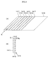
- FIGS. 3A and 3B are views illustrating the configuration of an integrated parallel-glass unit according to an embodiment of the present invention.
- FIG. 4 is a view illustrating the operation of an integrated parallel-glass unit according to an embodiment of the present invention.
- FIG. 5 is a view showing another arrangement example of the integrated parallel-glass unit
- FIG. 6 is a view showing the arrangement of light beams on an exposure surface
- FIG. 7 is a view showing the general configuration of another exposure apparatus according to an embodiment of the present invention.
- FIG. 1 is a view showing the general configuration of an exposure apparatus according to an embodiment of the present invention
- FIGS. 2A and 2B are views illustrating a light source optical system according to an embodiment of the present invention
- FIGS. 3A and 3B are views illustrating the configuration of an integrated parallel-glass unit 14 L according to an embodiment of the present invention
- FIG. 4 is a view illustrating the operation of an integrated parallel-glass unit according to an embodiment of the present invention
- FIG. 5 is a view showing another arrangement example of an integrated parallel-glass unit
- FIG. 6 is a view showing the arrangement of light beams in an exposure surface
- FIG. 7 is a view showing the general configuration of another exposure apparatus according to an embodiment of the present invention.
- An exposure apparatus 200 includes a light source optical system 1 , a mirror 100 , a long-focus lens 3 , a mirror 4 , a polygon mirror 5 , an f ⁇ lens 6 , a return mirror 62 , a cylindrical lens 61 , a stage 7 , and a control circuit 9 .
- the light source optical system 1 includes a multiple-parallel-beam generating unit 11 and an integrated parallel-glass unit 14 .
- An exposure substrate 8 is fixed on the stage 7 .
- FIG. 2A is a front view (as seen from the mirror 100 side; the left side in the drawing corresponds to the upper side) of the light source optical system 1 .
- FIG. 2B is a schematic sectional plan view of the light source optical system 1 as seen from the side surface.
- the multiple-parallel-beam generating unit 11 includes a holder 110 formed of a copper material, semiconductor lasers (hereinafter, referred to as the “LDs”) 12 , and aspherical lenses 13 .
- LDs semiconductor lasers
- Aspherical lenses 13 In the holder 110 , 16 (8 on the left and 8 on the right) LDs each having an outer diameter of 5 to 6 mm and mounted on a can package at a pitch of 13 mm, and 8 LDs are respectively arranged in the x direction and y direction, that is, a total of 128 LDs are arranged.
- each LD 12 is arranged so as to be shifted by 13/8 mm from the LD 12 of an adjacent row.
- each LD 12 outputs laser light with a full angle of divergence at half maximum (divergence angle) in the x direction of about 22 degrees, and a divergence angle in the y direction of about 8 degrees.
- the integrated parallel-glass unit 14 includes parallel glasses 1401 to 1408 (hereinafter, this group of glasses will be referred to as “integrated parallel-glass unit 14 R”) and parallel glasses 1411 to 1418 (hereinafter, this group of glasses will be referred to as “integrated parallel-glass unit 14 L”), each of which is a parallelogram in cross section.
- FIGS. 3A and 3B are views illustrating the configuration of the integrated parallel-glass unit 14 on the left side in the drawing, of which FIG. 3A is a view showing the entire integrated parallel-glass unit 14 L, and FIG. 3B is a view as seen from the arrow K in FIG. 3A .
- Each individual parallel glass is a parallelogram whose one vertex angle is 45 degrees.
- rectangular grooves G are formed on the right side surface of the parallel glass 1411 .
- the width W of the grooves G is 1.6 mm.
- the other surfaces of the parallel glass 1411 are flat.
- the grooves G are also formed on the right side surfaces of the parallel glasses 1412 to 1417 (however, the grooves G are shifted from each other by 13/8 mm in the height direction). In contrast, all the surfaces of the parallel glass 1418 are flat.
- the parallel glasses 1401 to 1408 and 1411 to 1418 are held in direct contact with each other by means of so-called optical contact.
- optical contact makes it possible to achieve a considerable improvement in the parallelism of parallel beams 10 , and also eliminates reflection loss resulting from a mismatch in refractive index between an adhesive and glass. Further, there is no fear of degradation of an adhesive, which occurs when parallel beams 10 A are ultraviolet light or near ultraviolet light.
- laser light 10 A 1 which corresponds to laser light 10 A at the left end made to enter the parallel glass 1411 from the lower part of the drawing, undergoes total reflection at AL 1 as the boundary with air, and travels rightward in the drawing. Subsequently, the laser light 10 A 1 passes through the parallel glasses 1412 to 1418 , undergoes total reflection at BL 1 as the boundary with air to travel upward in the drawing, and emerges from the upper surface of the parallel glass 1418 . Further, a parallel beam 10 A 2 , which enters the parallel glass 1412 from in the lower part of the drawing and located second from the left, undergoes total reflection at AL 2 corresponding to grooves formed in the parallel glass 1411 , and then travels rightward in the drawing.
- the parallel beam 10 A 2 passes through the parallel glasses 1413 to 1418 , undergoes total reflection at BL 2 as the boundary with air to travel upward in the drawing, and emerges from the upper surface of the parallel glass 1418 .
- the parallel beam 10 A undergoes total reflection at that location. That is, incident parallel beams 10 A with a pitch Px of 13 mm emerge from the parallel glass 1418 as parallel beams 10 with a pitch Px′ (in this case, 1 mm).
- incident parallel beams 10 A with a pitch Px of 13 mm emerge from the parallel glass 1408 as parallel beams 10 with a pitch Px′ (in this case, 1 mm).
- Px′ in this case, 1 mm.
- the overlapping portions of the parallel glass 1408 and parallel glass 1418 are fixed in an engaged manner (each edge is formed in a comb-tooth shape and engaged), so there is no fear of the optical path of the parallel beams 10 A being disturbed.
- each groove G is rectangular in this embodiment, since it suffices to realize total reflection of light beams trying to enter the grooves G, the shape of the groove G may be a V shape, a U shape, or the other such shape as long as an air space larger than the width W can be formed.
- the spacing dp may be set as 8.5 mm.
- the incident surface and the emergent surface be parallel to each other (the parallelism between adjacent reflection surfaces be within 30 seconds for practical use, preferably 10 seconds).
- the parallel glasses it is relatively easy to process the parallel glasses to a parallelism on the order of 1 second.
- the loss at reflection is 0 since the reflection is total reflection.
- anti-reflection coating is applied to the incident surface and the emergent surface, since the resulting reflection is normal incidence reflection, the loss at these surfaces can be made to 0.2% or less.
- a transparent adhesive may be used instead of achieving direct contact between the parallel glasses 1401 to 1408 and 1411 to 1418 by means of optical contact.
- silica exhibits extremely small thermal expansion in comparison to other glass materials, if silica glass is used as the glass, when optical contact is employed, there is little fear of the parallel glasses coming out of optical contact due to thermal change, thereby making it possible to produce a stable high-performance parallel glass unit.
- parallel glasses 1401 to 1408 and 1411 to 1418 may be formed of a transparent material other than glass.
- the long-focus lens 3 includes spherical type lenses 31 , 32 , 33 , and a cylindrical lens 34 having power in the x direction and with a focal length fc.
- the lenses 31 , 32 , 33 are each formed by multiple lenses, and the overall focal length is fo.
- the laser beams outputted from the LDs 12 and made to enter the aspherical lenses 13 emerge from the spherical lenses 13 as mutually parallel beams 10 A in a matrix form with a pitch (Px) of 13 mm in the x direction and a pitch (Py) of 13 mm in the y direction.
- the respective laser beams collimated by the spherical lenses 13 have an elliptic intensity distribution with a diameter of about 4 mm in the x direction and a diameter of about 1.5 mm in the y direction.
- the incident parallel beams 10 A on the integrated parallel-glass unit 14 emerge from the integrated parallel-glass unit 14 as multiple parallel beams 10 in a matrix form with Py (pitch in the y direction) of 13 mm and a pitch (Px′) in the x direction of 1 mm, and is made to enter the long-focus lens 3 with a focal length of about 20 m.
- the principal rays of the respective beams are reflected by the mirror 4 to be converged onto a mirror surface of the polygon mirror 5 .
- the focal length is relatively long at 20 m, the beam diameters of the respective beams have been enlarged to about 10 mm.
- the polygon mirror 5 is rotating at a rotational speed of about 5,000 rpm ( ⁇ rad ⁇ s ⁇ 1 in terms of angular velocity). Reflected light is made to enter the f ⁇ lens 6 , and after reflection by the mirror 62 , transmits through the cylindrical lens 61 having a focal length f ⁇ C, and then, as shown in FIG. 6 , forms the images of spots 80 , which are formed by beams emitted from the respective LDs 12 , onto the exposure surface of the exposure substrate 8 mounted on the stage 7 .
- the spots on the substrate are scanned at a speed of 2f ⁇ (mm/s) in the ⁇ y direction of the coordinates on the stage shown in FIG. 1 .
- the stage 7 is subjected to scanning in the ⁇ x direction in synchronism with this scanning, and the respective LDs 12 are ON-OFF controlled on the basis of drawing data previously stored in the control circuit 9 , thus enabling formation of a desired pattern on the exposure substrate 8 by exposure.
- Dx, Dy are 4, 1.5 mm (e ⁇ 2 ), respectively, and the focal length of each of the above-mentioned lenses is determined so that dx, dy become about 20 ⁇ m.
- FIG. 7 is a view of another exposure apparatus according to an embodiment of the present invention.
- the multiple-parallel-beam generating unit 11 incorporates violet semiconductor laser (407 nm) LDs.
- a multiple-parallel-beam generating unit 11 ′ incorporates ultraviolet semiconductor laser (375 nm) LDs.
- Parallel laser light beams with a pitch of 13 mm in the x-y direction emerge from the respective multiple-parallel-beam generating units 11 , 11 ′ so as to be parallel to each other.
- Multiple ultraviolet LD beams of 375 nm are reflected by a mirror 15 , and pass through a dichroic mirror 16 .
- multiple violet LD beams of 407 nm pass through an optical path that substantially completely coincides with that of the multiple beams of 375 nm.
- the placement of the LD light sources of 407 nm and 375 nm may be reversed.
- the dichroic mirror 16 transmits the beams of 407 nm and reflects the beams of 375 nm.
- the multiple beams of both wavelengths are together made to enter the parallel glass unit 14 that has been described in detail above.
- the pitch in the x direction of the emergent beams is compressed to 1 mm.
- the long-focus lens 3 with an aperture of about 120 mm in diameter is subjected to color correction with respect to both the wavelengths of 375 nm and 407 nm, the principal rays of the multiple beams of both wavelengths transmitted through the long-focus lens 3 coincide with each other on the polygon mirror 5 with respect to the y direction (horizontal direction).
- the beams that have been arranged at a pitch of 1 mm as described above are converged and condensed onto the same position on the polygon mirror for both the wavelengths at a magnification fc/fo determined by the focal length fo of the spherical lens system of the long-focus lens 3 and the focal length fc of the color-corrected cylindrical lens corresponding to the fourth group from the front end.
- the beams of both wavelengths reflected by the polygon mirror 5 transmit through the f ⁇ lens 6 .
- the stage 7 mounted on the exposure substrate 8 is moved in the direction indicated by the arrow in FIG. 6 .
- the respective LDs 12 are turned ON/OFF from the controller 9 at a timing determined by the arrangement positions of the respective LDs and desired drawing information, thereby forming a desired drawing pattern on the substrate 8 by exposure at two wavelengths simultaneously.
- the exposure apparatus enables maskless exposure to be performed simultaneously by using LDs of wavelengths near the h-line and i-line of a mercury lamp used in the mask exposure apparatus of the related art, and allows exposure to be performed in a satisfactory manner by using an inexpensive photoresist used in the related art.
Abstract
Description
dp=(Px−Px′)/√2
dx=Dxfcfθc/(fofθ)
dy=Dyfθc/fo
PEx=Px′fθ/fo
PEy=Pyfθcfc/(fofθ)
dy=4fθλ/(πDy)
dx=Dxfcfθc/(fofθ)
wherein dx, dy are substantially the same.
Claims (13)
Applications Claiming Priority (2)
| Application Number | Priority Date | Filing Date | Title |
|---|---|---|---|
| JP2006150431A JP4302716B2 (en) | 2006-05-30 | 2006-05-30 | Optical beam axis-to-axis pitch conversion apparatus and substrate exposure apparatus |
| JP2006-150431 | 2006-05-30 |
Publications (2)
| Publication Number | Publication Date |
|---|---|
| US20070279609A1 US20070279609A1 (en) | 2007-12-06 |
| US8089614B2 true US8089614B2 (en) | 2012-01-03 |
Family
ID=38650743
Family Applications (1)
| Application Number | Title | Priority Date | Filing Date |
|---|---|---|---|
| US11/755,361 Active 2029-06-17 US8089614B2 (en) | 2006-05-30 | 2007-05-30 | Device for changing pitch between light beam axes, and substrate exposure apparatus |
Country Status (6)
| Country | Link |
|---|---|
| US (1) | US8089614B2 (en) |
| JP (1) | JP4302716B2 (en) |
| KR (1) | KR101342473B1 (en) |
| CN (1) | CN101082780B (en) |
| DE (1) | DE102007024961A1 (en) |
| HK (1) | HK1115919A1 (en) |
Families Citing this family (3)
| Publication number | Priority date | Publication date | Assignee | Title |
|---|---|---|---|---|
| JP6288995B2 (en) * | 2013-09-06 | 2018-03-07 | キヤノン株式会社 | Optical scanning apparatus and image forming apparatus |
| CN106537224B (en) * | 2014-04-15 | 2019-11-26 | 荷兰应用科学研究会(Tno) | Photohead, exposure device and the method for operating photohead |
| JPWO2016098174A1 (en) * | 2014-12-15 | 2017-09-28 | ギガフォトン株式会社 | Laser irradiation device |
Citations (4)
| Publication number | Priority date | Publication date | Assignee | Title |
|---|---|---|---|---|
| US4690490A (en) * | 1983-09-27 | 1987-09-01 | Kei Mori | Light diverting device |
| US5890796A (en) * | 1997-01-16 | 1999-04-06 | Ford Global Technologies, Inc. | Laser illuminated lighting system utilizing a diffractive optical element |
| US20050219496A1 (en) * | 2004-03-31 | 2005-10-06 | Hitachi Via Mechanics Ltd. | Pattern exposure method and pattern exposure apparatus |
| US20060098700A1 (en) * | 2002-05-22 | 2006-05-11 | Oseir Oy | Method and a laser device for producing high optical power density |
-
2006
- 2006-05-30 JP JP2006150431A patent/JP4302716B2/en not_active Expired - Fee Related
-
2007
- 2007-05-22 KR KR1020070049791A patent/KR101342473B1/en not_active IP Right Cessation
- 2007-05-28 CN CN2007101046731A patent/CN101082780B/en not_active Expired - Fee Related
- 2007-05-30 US US11/755,361 patent/US8089614B2/en active Active
- 2007-05-30 DE DE102007024961A patent/DE102007024961A1/en not_active Withdrawn
-
2008
- 2008-06-03 HK HK08106172.9A patent/HK1115919A1/en not_active IP Right Cessation
Patent Citations (5)
| Publication number | Priority date | Publication date | Assignee | Title |
|---|---|---|---|---|
| US4690490A (en) * | 1983-09-27 | 1987-09-01 | Kei Mori | Light diverting device |
| US5890796A (en) * | 1997-01-16 | 1999-04-06 | Ford Global Technologies, Inc. | Laser illuminated lighting system utilizing a diffractive optical element |
| US20060098700A1 (en) * | 2002-05-22 | 2006-05-11 | Oseir Oy | Method and a laser device for producing high optical power density |
| US20050219496A1 (en) * | 2004-03-31 | 2005-10-06 | Hitachi Via Mechanics Ltd. | Pattern exposure method and pattern exposure apparatus |
| JP2005316349A (en) | 2004-03-31 | 2005-11-10 | Hitachi Via Mechanics Ltd | Pattern exposure method and pattern exposure apparatus |
Also Published As
| Publication number | Publication date |
|---|---|
| CN101082780A (en) | 2007-12-05 |
| JP4302716B2 (en) | 2009-07-29 |
| DE102007024961A1 (en) | 2007-12-06 |
| HK1115919A1 (en) | 2008-12-12 |
| CN101082780B (en) | 2011-03-30 |
| KR101342473B1 (en) | 2013-12-17 |
| US20070279609A1 (en) | 2007-12-06 |
| KR20070115635A (en) | 2007-12-06 |
| JP2007322543A (en) | 2007-12-13 |
Similar Documents
| Publication | Publication Date | Title |
|---|---|---|
| KR101649812B1 (en) | An optical projection array exposure system | |
| KR100827874B1 (en) | Exposure apparatus, method for manufacturing thereof, method for exposing, method for manufacturing microdevice, and method for manufacturing device | |
| KR101662330B1 (en) | Illumination optical system, illumination optical apparatus, exposure apparatus, and device manufacturing method | |
| TWI448833B (en) | An exposure device and a light source device | |
| JP4410134B2 (en) | Pattern exposure method and apparatus | |
| JP2005316349A (en) | Pattern exposure method and pattern exposure apparatus | |
| JP2006261155A (en) | Aligner and exposure method | |
| US6980366B2 (en) | Projecting exposure apparatus | |
| JP2005032909A (en) | Lighting optical system and aligner using it | |
| US8089614B2 (en) | Device for changing pitch between light beam axes, and substrate exposure apparatus | |
| JP2009210726A (en) | Maskless exposure apparatus | |
| JP2008242238A (en) | Exposure apparatus | |
| US7755741B2 (en) | Substrate exposure apparatus and illumination apparatus | |
| JP2009301066A (en) | Pattern exposure method and pattern exposure apparatus | |
| JP4323335B2 (en) | Image exposure method and apparatus | |
| WO2009128293A1 (en) | Spatial light modulation unit, lighting optical system, exposure apparatus and method for manufacturing device | |
| JP4208141B2 (en) | Image exposure method and apparatus | |
| US20210063884A1 (en) | Mask-less laser direct imaging system | |
| CN111505908B (en) | Illumination optical system, exposure apparatus, and article manufacturing method | |
| JP2011222841A (en) | Spatial light modulation unit, illumination optical system, exposure device, and device manufacturing method | |
| JP2009244711A (en) | Exposure device | |
| WO2013115208A1 (en) | Transmission optical system, illumination optical system, exposure device, and device manufacturing method | |
| JP2006047384A (en) | Aligner | |
| CN117289553A (en) | Alignment adjusting system of MLA lens of lithography machine | |
| JP2004029234A (en) | Optical system and apparatus for projection exposure |
Legal Events
| Date | Code | Title | Description |
|---|---|---|---|
| AS | Assignment |
Owner name: HITACHI VIA MECHANICS, LTD., JAPAN Free format text: ASSIGNMENT OF ASSIGNORS INTEREST;ASSIGNORS:OSHIDA, YOSHITADA;NAITO, YOSHITATSU;SUZUKI, MITUHIRO;AND OTHERS;REEL/FRAME:019618/0431 Effective date: 20070510 |
|
| AS | Assignment |
Owner name: HITACHI VIA MECHANICS, LTD., JAPAN Free format text: CORRECTIVE ASSIGNMENT TO CORRECT THE SPELLING OF THE FIRST NAME OF THE THIRD ASSIGNOR'S PREVIOUSLY RECORDED ON REEL 019618 FRAME 0431.;ASSIGNORS:OSHIDA, YOSHITADA;NAITO, YOSHITATSU;SUZUKI, MITSUHIRO;AND OTHERS;REEL/FRAME:020338/0174 Effective date: 20070510 Owner name: HITACHI VIA MECHANICS, LTD., JAPAN Free format text: CORRECTIVE ASSIGNMENT TO CORRECT THE SPELLING OF THE FIRST NAME OF THE THIRD ASSIGNOR'S PREVIOUSLY RECORDED ON REEL 019618 FRAME 0431;ASSIGNORS:OSHIDA, YOSHITADA;NAITO, YOSHITATSU;SUZUKI, MITSUHIRO;AND OTHERS;REEL/FRAME:020338/0174 Effective date: 20070510 |
|
| STCF | Information on status: patent grant |
Free format text: PATENTED CASE |
|
| FEPP | Fee payment procedure |
Free format text: PAYOR NUMBER ASSIGNED (ORIGINAL EVENT CODE: ASPN); ENTITY STATUS OF PATENT OWNER: LARGE ENTITY |
|
| AS | Assignment |
Owner name: VIA MECHANICS, LTD., JAPAN Free format text: CHANGE OF NAME;ASSIGNOR:HITACHI VIA MECHANICS, LTD.;REEL/FRAME:032600/0580 Effective date: 20131101 |
|
| FPAY | Fee payment |
Year of fee payment: 4 |
|
| AS | Assignment |
Owner name: ADTEC ENGINEERING CO., LTD., JAPAN Free format text: ASSIGNMENT OF ASSIGNORS INTEREST;ASSIGNOR:VIA MECHANICS, LTD.;REEL/FRAME:047412/0658 Effective date: 20180119 |
|
| MAFP | Maintenance fee payment |
Free format text: PAYMENT OF MAINTENANCE FEE, 8TH YEAR, LARGE ENTITY (ORIGINAL EVENT CODE: M1552); ENTITY STATUS OF PATENT OWNER: LARGE ENTITY Year of fee payment: 8 |
|
| MAFP | Maintenance fee payment |
Free format text: PAYMENT OF MAINTENANCE FEE, 12TH YEAR, LARGE ENTITY (ORIGINAL EVENT CODE: M1553); ENTITY STATUS OF PATENT OWNER: LARGE ENTITY Year of fee payment: 12 |