US8080984B1 - Replica transistor voltage regulator - Google Patents
Replica transistor voltage regulator Download PDFInfo
- Publication number
- US8080984B1 US8080984B1 US12/154,169 US15416908A US8080984B1 US 8080984 B1 US8080984 B1 US 8080984B1 US 15416908 A US15416908 A US 15416908A US 8080984 B1 US8080984 B1 US 8080984B1
- Authority
- US
- United States
- Prior art keywords
- output
- source
- voltage
- coupled
- voltage regulator
- Prior art date
- Legal status (The legal status is an assumption and is not a legal conclusion. Google has not performed a legal analysis and makes no representation as to the accuracy of the status listed.)
- Active, expires
Links
Images


Classifications
-
- G—PHYSICS
- G05—CONTROLLING; REGULATING
- G05F—SYSTEMS FOR REGULATING ELECTRIC OR MAGNETIC VARIABLES
- G05F1/00—Automatic systems in which deviations of an electric quantity from one or more predetermined values are detected at the output of the system and fed back to a device within the system to restore the detected quantity to its predetermined value or values, i.e. retroactive systems
- G05F1/10—Regulating voltage or current
- G05F1/46—Regulating voltage or current wherein the variable actually regulated by the final control device is dc
- G05F1/56—Regulating voltage or current wherein the variable actually regulated by the final control device is dc using semiconductor devices in series with the load as final control devices
Definitions
- the present invention relates generally to voltage regulators, and more particularly to a circuit and method to substantially prevent or interrupt reverse current flow into a voltage regulator from an output thereof.
- Voltage regulator circuits or voltage regulators are widely used in many applications to provide a nearly constant output voltage at a desired level that is substantially independent of a poorly specified and often fluctuating input voltage and output conditions (i.e., variation in a load current).
- One type of voltage regulator is a replica transistor voltage regulator.
- a replica transistor voltage regulator In a replica transistor voltage regulator a voltage established in a replica leg using a dummy or replicated load and is replicated in an output leg to provide a desired output voltage (V out ).
- the output leg is made using larger semiconductor devices capable of carrying higher current demanded by devices or circuits coupled to an output-node of the regulator.
- V out from the output-node in the output leg is regulated substantially independent of an output load by forcing the output leg to track voltage in the replica leg as closely as possible.
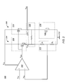
- the voltage regulator 100 includes an operational amplifier (OPAMP 102 ) having a non-inverting input coupled to a reference voltage (V ref ), a replica leg 104 coupled between a voltage source (V pwr ) and a circuit ground 106 , and an output leg 108 coupled between V pwr and an output-node 110 .
- OPAMP 102 operational amplifier having a non-inverting input coupled to a reference voltage (V ref ), a replica leg 104 coupled between a voltage source (V pwr ) and a circuit ground 106 , and an output leg 108 coupled between V pwr and an output-node 110 .
- the replica leg 104 includes a replica transistor 112 coupled to and controlled by a voltage (V gate ) output from the OPAMP 102 , and a replicated or dummy load 114 , represented here as a resistance (R rep ) and a parallel capacitance (C rep ), through which the replica transistor 112 is coupled to ground 106 .
- the output leg 108 includes a second, typically larger output transistor 116 coupled to the OPAMP 102 and controlled by V gate , and the output-node 110 through which the output transistor is coupled to an output load, represented here by a current (I load ) and a capacitance (C load ).
- the OPAMP 102 is configured in negative feedback so that the output of the OPAMP, V gate , forces the V out voltage to the same voltage as a voltage (V rep ) in the replica leg 102 .
- the replica transistor 112 and output transistor 116 are ratioed so that the current provided to output leg 108 is much larger than that of the replica leg 104 at the desired output voltage.
- An alternative voltage regulator architecture further includes a current conveyor coupled between the first leg of the circuit and an output-node in the replica leg.
- the current conveyor provides feedback between an output voltage (V out ) and an operational amplifier (OPAMP) at the input to the voltage regulator.
- the OPAMP controls current supplied to the current conveyor based on a comparison between a reference voltage and a feedback voltage.
- the current conveyor forces V out to follow the input or source voltage.
- voltage regulators including current conveyors provide regulation with a relatively good accuracy in output voltage, typically varying by as little as 5%, they too suffer from a number of drawbacks or disadvantages including poor headroom of less than about 50 millivolts (mV), and a poor power supply rejection ratio (PSRR), typically of about ⁇ 5 decibels (dB) or greater.
- mV millivolts
- PSRR power supply rejection ratio
- headroom it is meant a maximum allowable shift in input or source voltage for which the voltage regulator can adjust or compensate in the output voltage V out .
- PSRR is a term widely used in the field of electronics to quantify noise coupled from a power supply to a considered node, such as the output-node. More fundamentally, the current conveyor architecture requires a relatively large area on a die or substrate on which it is fabricated, utilizing from about 133K to 150K square microns ( ⁇ m 2 ), making it unsuitable for use in many integrated circuits (ICs).
- the present invention provides a solution to these and other problems, and offers further advantages over conventional voltage regulators and methods of operating the same.
- the present invention is directed to a voltage regulator for regulating a voltage (V out ) at an output-node of the regulator in response to a comparison between a reference voltage (V ref ) and a feedback voltage (V fbk ) from the output-node.
- the voltage regulator comprises: (i) an operational amplifier (OPAMP) having a non-inverting input coupled to V ref ; (ii) an output source follower coupled to and controlled by an output of the OPAMP, the output source follower including a drain coupled to a voltage source and a source coupled to the output-node of the voltage regulator; (iii) a replica source follower coupled to and controlled by the output of the OPAMP in parallel with the output source follower, the replica source follower including a drain coupled to the voltage source and a source coupled to a circuit ground through a resistor network; and (iv) a feedback circuit extending from the output-node through a feedback resistor to the source of the replica source follower and through at least a first resistor of the resistor network to an inverting input of the OPAMP to couple V fbk thereto to regulate V out the output-node in response to a comparison between V fbk and V ref .
- the feedback resistor is a
- the voltage regulator is a replica transistor voltage regulator comprising a replica leg including the replica source follower and the resistor network, and an output leg comprising the output source follower and further comprising a leaker transistor coupled between the source of the output source follower and circuit ground.
- the leaker transistor comprises a drain coupled to the source of the output source follower and a source coupled to circuit ground. The leaker transistor is controlled by a DC bias voltage to leak current from the output-node to provide a constant minimum current flowing in the output source follower, thereby improving circuit stability and avoid floating nodes.
- the voltage regulator of the present invention is capable of providing a V out that varies by 4.5% or less, a power supply rejection ratio (PSRR) equal to or less than about ⁇ 20 decibels (dB), and maximum headroom of at least 280 millivolts (mV).
- PSRR power supply rejection ratio
- dB decibels
- mV millivolts
- the voltage regulator can be implemented on a substrate utilizing an area of less than about 100K microns ( ⁇ m 2 ), making it particularly suitable for integrated circuit (IC) applications.
- the voltage regulator comprises a feedback circuit including a feedback transistor coupled between the source of the replica source follower and the output-node.
- the feedback transistor is controlled by a DC biasing voltage that can be varied to adjust a magnitude of the feedback voltage (V fbk ).
- the feedback transistor is connected as a source follower having a source coupled to the source of the replica source follower and a drain coupled to the source of the output source follower. More preferably, the feedback transistor further comprises a bulk terminal coupled to the source thereof to improve the stability of the feedback circuit.
- the invention is directed to a method of operating a replica transistor voltage regulator to improve accuracy, while providing a good power supply rejection ratio (PSRR) and substantially no headroom limitations.
- the method includes the step of coupling a feedback voltage (V fbk ) from the output-node to an inverting input of an OPAMP through a feedback resistor coupled between the output-node and a source of a replica source follower.
- the feedback circuit comprises a feedback transistor coupled between the output-node and the source of the replica source follower, and the method includes the further step of controlling a biasing voltage to the feedback transistor to adjust a magnitude of V fbk .
- FIG. 1 is a simplified schematic diagram of a conventional replica transistor voltage regulator according to an embodiment of the present invention
- FIG. 2 is a simplified schematic diagram of a voltage regulator according to an embodiment of the present invention.
- FIG. 3 is a simplified schematic diagram of a voltage regulator according to another embodiment of the present invention.
- the present invention is directed to a replica transistor voltage regulator having a feedback loop between sources of an output source follower and a replica source follower.
- the voltage regulator and method of the present invention are particularly useful in battery operated devices, such as a wireless computer mouse and other like devices, which include integrated voltage regulators fabricated on a common semiconductor die or substrate with integrated circuits (ICs) of the devices.
- battery operated devices such as a wireless computer mouse and other like devices, which include integrated voltage regulators fabricated on a common semiconductor die or substrate with integrated circuits (ICs) of the devices.
- ICs integrated circuits
- the voltage regulator circuit or voltage regulator of the present invention includes a feedback circuit between a source of an output source follower in an output leg and a source of a replica source follower in a replica leg.
- the voltage regulator provides exceptional accuracy and a good power supply rejection ratio (PSRR), while substantially eliminating headroom issues and reducing the size of the voltage regulator on a semiconductor die or substrate as compared to conventional voltage regulators having current conveyor architectures.
- PSRR power supply rejection ratio
- FIGS. 2 and 3 The voltage regulator and methods for operating the same according to various embodiments of the present invention will now be described in detail with reference to FIGS. 2 and 3 .
- FIGS. 2 and 3 For purposes of clarity, many of the details of integrated circuit design in general and design of voltage regulators in particular that are widely known and are not relevant to the present invention have been omitted from the following description.
- the voltage regulator 200 generally includes an operational amplifier (OPAMP 202 ) having a non-inverting input coupled to a predetermined reference voltage (V ref ), a replica leg 204 and an output leg 206 to provide a regulated output voltage (V out ) to a circuit or load (not shown) coupled to the voltage regulator.
- OPAMP 202 operational amplifier having a non-inverting input coupled to a predetermined reference voltage (V ref ), a replica leg 204 and an output leg 206 to provide a regulated output voltage (V out ) to a circuit or load (not shown) coupled to the voltage regulator.
- the replica leg 204 includes a first metal-oxide-semiconductor (MOS) transistor 208 connected as a source follower and including a gate coupled to an output (V gate ) of the OPAMP 202 , a drain coupled to a voltage source (V pwr ), and a source coupled through a resistor network 210 to a circuit ground 212 and through at least a first resistor (R 1 ) of the resistor network to an inverting input of the OPAMP.
- MOS metal-oxide-semiconductor
- the output leg 206 includes a second MOS transistor 214 connected as a source follower and including a gate coupled to the output (V gate ) of the OPAMP 202 , a drain coupled to the voltage source (V pwr ) and a source coupled to an output node 216 of the voltage regulator 200 .
- the second MOS transistor or output source follower 214 is scaled to be n times as large as the first MOS transistor or replica source follower 208 . That is a ratio of a power or current carrying capacity of the output source follower 214 to the replica source follower 208 can be n:1 where n is greater than 1, thereby enabling the output source follower to provide a desired current for the output leg 208 as well as a load device (not shown) coupled to the output-node 216 .
- the output leg 206 further includes a leaker transistor 218 coupled between the source of the output source follower 214 and circuit ground 212 .
- the leaker transistor 218 comprises a drain coupled to the source of the output source follower 214 and a source coupled to circuit ground 212 , and is controlled by a DC bias voltage (bias) to provide a constant minimum current flowing in the output source follower, thereby improving circuit stability and avoid floating nodes.
- bias DC bias voltage
- one or more of the MOS transistors of the replica source follower 208 , output source follower 214 and leaker transistor 218 further include a bulk terminal coupled to the source to improve the stability of the voltage regulator 200 .
- the voltage regulator 200 further includes a feedback loop or circuit extending from the output-node 216 through a feedback resistor (R fbk 220 ) to the source of the replica source follower 208 and through the first resistor (R 1 ) of the resistor network 210 to the inverting input of the OPAMP 202 .
- the feedback circuit couples a feedback voltage (V fbk ) to the inverting input of the OPAMP 202 to control the output source follower 214 in response to a comparison between V fbk and V ref , thereby regulating the voltage (V out ) at the output-node 216 .
- the value of resistance selected for the feedback resistor 220 will depend on a number of factors including, a desired accuracy of regulation and a desired stability of the voltage regulator.
- the smaller the feedback resistor 220 the larger the magnitude of the feedback (V fbk ) and the more accurate the voltage regulation achieved.
- the larger V fbk the less stable the voltage regulator will be, and therefore there is a tradeoff between regulator accuracy and stability.
- the feedback resistor 220 is a small resistor having a resistance of about 100 Ohms or less, and more preferably having a resistance in the tens of Ohms or less.
- the value of resistance selected for the resistor network 210 and a ratio of the resistance of resistor (R 1 ) to a resistance of other resistors in the resistor network but not in a feedback path, represented in this figure by resistor (R 2 ), will depend on a number of factors including, a desired amount or magnitude of feedback, the resistance of the feedback resistor 220 , and a desired current flow through the replica leg 204 .
- the resistor network 210 can include a total resistance on the order of several tens of Ohms to several hundreds of Ohms, and ratio of resistance of R 1 to R 2 of from about 0, that is no resistor R 1 , to about 1:10.
- the feedback resistor (R fbk ) in the feedback loop or circuit is replaced with a feedback transistor 222 coupled between the output-node 216 and the first resistor (R 1 ) of the resistor network 210 .
- the feedback transistor 222 is a MOS transistor including a control node or gate coupled to and controlled by a second DC bias voltage (bias 2 ) different from the first DC bias voltage (bias 1 ) used to control the leaker transistor 218 .
- bias 2 second DC bias voltage
- the feedback MOS transistor can include a bulk terminal coupled to a source terminal of the transistor to improve the stability of the feedback circuit.
- the voltage regulator of the present can also be implemented using, for example, bipolar NPN transistors in a common collector configuration.
- Advantages of the circuit of the present invention over previous or conventional approaches include: (i) high accuracy having an output voltage that varies by about 4.2% or less; (ii) a good PSRR of about ⁇ 20 dB or less; (iii) substantially no headroom limitations having a margin of 280 millivolts (mV) or more; and (iv) a small silicon area on the substrate on which it is fabricated utilizing less than about 100K ⁇ m 2 or at least 30% less than existing architectures.
Abstract
Description
Claims (19)
Priority Applications (1)
| Application Number | Priority Date | Filing Date | Title |
|---|---|---|---|
| US12/154,169 US8080984B1 (en) | 2007-05-22 | 2008-05-21 | Replica transistor voltage regulator |
Applications Claiming Priority (2)
| Application Number | Priority Date | Filing Date | Title |
|---|---|---|---|
| US93121607P | 2007-05-22 | 2007-05-22 | |
| US12/154,169 US8080984B1 (en) | 2007-05-22 | 2008-05-21 | Replica transistor voltage regulator |
Publications (1)
| Publication Number | Publication Date |
|---|---|
| US8080984B1 true US8080984B1 (en) | 2011-12-20 |
Family
ID=43357342
Family Applications (2)
| Application Number | Title | Priority Date | Filing Date |
|---|---|---|---|
| US12/009,877 Active 2029-01-31 US7859240B1 (en) | 2007-05-22 | 2008-01-22 | Circuit and method for preventing reverse current flow into a voltage regulator from an output thereof |
| US12/154,169 Active 2029-10-26 US8080984B1 (en) | 2007-05-22 | 2008-05-21 | Replica transistor voltage regulator |
Family Applications Before (1)
| Application Number | Title | Priority Date | Filing Date |
|---|---|---|---|
| US12/009,877 Active 2029-01-31 US7859240B1 (en) | 2007-05-22 | 2008-01-22 | Circuit and method for preventing reverse current flow into a voltage regulator from an output thereof |
Country Status (1)
| Country | Link |
|---|---|
| US (2) | US7859240B1 (en) |
Cited By (20)
| Publication number | Priority date | Publication date | Assignee | Title |
|---|---|---|---|---|
| US20100253303A1 (en) * | 2009-04-01 | 2010-10-07 | Taiwan Semiconductor Manufacturing Company, Ltd. | Voltage regulator with high accuracy and high power supply rejection ratio |
| US20110089916A1 (en) * | 2009-10-20 | 2011-04-21 | Taiwan Semiconductor Manufacturing Company, Ltd. | Ldo regulators for integrated applications |
| US20110133719A1 (en) * | 2009-12-04 | 2011-06-09 | Advance Micro Devices, Inc. | Voltage reference circuit operable with a low voltage supply and method for implementing same |
| US20110316519A1 (en) * | 2010-06-25 | 2011-12-29 | David Schie | Load Switch |
| US20120086490A1 (en) * | 2010-10-11 | 2012-04-12 | Samsung Electronics Co., Ltd. | Integrated circuit devices using power supply circuits with feedback from a replica load |
| US20120169305A1 (en) * | 2010-12-30 | 2012-07-05 | Samsung Electro-Mechanics., Ltd. | Multi-voltage regulator |
| US8351886B1 (en) * | 2010-02-04 | 2013-01-08 | Triquint Semiconductor, Inc. | Voltage regulator with a bandwidth variation reduction network |
| US20130221937A1 (en) * | 2012-02-24 | 2013-08-29 | Shouli Yan | Voltage Regulator with Adjustable Feedback |
| US20140253089A1 (en) * | 2013-03-08 | 2014-09-11 | Analog Devices Technology | Apparatus and methods for switching regulator current sensing |
| US9046905B2 (en) | 2013-03-08 | 2015-06-02 | Analog Devices Global | Apparatus and methods for bidirectional current sensing in a switching regulator |
| CN104793673A (en) * | 2014-01-22 | 2015-07-22 | 上海华虹集成电路有限责任公司 | LDO circuit applied to HSIC connector whole chip integration |
| CN105652942A (en) * | 2016-03-15 | 2016-06-08 | 西安紫光国芯半导体有限公司 | Voltage drop reduction device |
| US9461539B2 (en) | 2013-03-15 | 2016-10-04 | Taiwan Semiconductor Manufacturing Company, Ltd. | Self-calibrated voltage regulator |
| WO2017172346A1 (en) * | 2016-03-31 | 2017-10-05 | Micron Technology, Inc. | Apparatuses and methods for a load current control circuit for a source follower voltage regulator |
| US9791480B2 (en) | 2013-05-21 | 2017-10-17 | Analog Devices Global | Current sensing of switching power regulators |
| US20190302819A1 (en) * | 2018-03-28 | 2019-10-03 | Qualcomm Incorporated | Methods and apparatuses for multiple-mode low drop out regulators |
| US10461629B2 (en) * | 2018-02-19 | 2019-10-29 | Texas Instruments Incorporated | System and apparatus to provide current compensation |
| US20210184661A1 (en) * | 2019-12-13 | 2021-06-17 | Qualcomm Incorporated | Rail-to-rail source follower buffer for switching regulator driver supply |
| US20220283600A1 (en) * | 2021-03-04 | 2022-09-08 | United Semiconductor Japan Co., Ltd. | Voltage Regulator Providing Quick Response to Load Change |
| US11616505B1 (en) * | 2022-02-17 | 2023-03-28 | Qualcomm Incorporated | Temperature-compensated low-pass filter |
Families Citing this family (3)
| Publication number | Priority date | Publication date | Assignee | Title |
|---|---|---|---|---|
| US9582017B2 (en) | 2013-07-02 | 2017-02-28 | Stmicroelectronics Design And Application S.R.O. | Method of preventing inversion of output current flow in a voltage regulator and related voltage regulator |
| CN107919653B (en) | 2016-10-10 | 2022-01-11 | 恩智浦有限公司 | Reverse current protection circuit for switching circuit |
| US10630028B2 (en) | 2018-04-12 | 2020-04-21 | Cypress Semiconductor Corporation | Reverse overcurrent protection for universal serial bus type-C (USB-C) connector systems |
Citations (24)
| Publication number | Priority date | Publication date | Assignee | Title |
|---|---|---|---|---|
| US4851759A (en) | 1988-05-26 | 1989-07-25 | North American Philips Corporation, Signetics Division | Unity-gain current-limiting circuit |
| US4884161A (en) | 1983-05-26 | 1989-11-28 | Honeywell, Inc. | Integrated circuit voltage regulator with transient protection |
| US4893030A (en) | 1986-12-04 | 1990-01-09 | Western Digital Corporation | Biasing circuit for generating precise currents in an integrated circuit |
| US5637992A (en) | 1995-05-31 | 1997-06-10 | Sgs-Thomson Microelectronics, Inc. | Voltage regulator with load pole stabilization |
| US5661395A (en) | 1995-09-28 | 1997-08-26 | International Business Machines Corporation | Active, low Vsd, field effect transistor current source |
| US6157178A (en) | 1998-05-19 | 2000-12-05 | Cypress Semiconductor Corp. | Voltage conversion/regulator circuit and method |
| US6157176A (en) | 1997-07-14 | 2000-12-05 | Stmicroelectronics S.R.L. | Low power consumption linear voltage regulator having a fast response with respect to the load transients |
| US6222353B1 (en) | 2000-05-31 | 2001-04-24 | Philips Semiconductors, Inc. | Voltage regulator circuit |
| US6232757B1 (en) | 1999-08-20 | 2001-05-15 | Intel Corporation | Method for voltage regulation with supply noise rejection |
| US6249177B1 (en) | 2000-09-28 | 2001-06-19 | Cypress Semiconductor Corp. | Method, circuit and/or architecture for reducing gate oxide stress in low-voltage regulated devices |
| US6373231B1 (en) | 2000-12-05 | 2002-04-16 | Cypress Semiconductor Corp. | Voltage regulator |
| US6424131B1 (en) | 1999-06-18 | 2002-07-23 | Matsushita Electric Industrial Co., Ltd. | Output controller |
| US6441593B1 (en) | 2000-12-14 | 2002-08-27 | Cypress Semiconductor Corp. | Low noise switching regulator |
| US6501256B1 (en) | 2001-06-29 | 2002-12-31 | Intel Corporation | Trimmable bandgap voltage reference |
| US6522111B2 (en) | 2001-01-26 | 2003-02-18 | Linfinity Microelectronics | Linear voltage regulator using adaptive biasing |
| US6566851B1 (en) | 2000-08-10 | 2003-05-20 | Applied Micro Circuits, Corporation | Output conductance correction circuit for high compliance short-channel MOS switched current mirror |
| US6601936B2 (en) | 2000-11-14 | 2003-08-05 | Cypress Semiconductor Corp. | Real time adaptive inkjet temperature regulation controller |
| US6661214B1 (en) | 2001-09-28 | 2003-12-09 | Itt Manufacturing Enterprises, Inc. | Droop compensation circuitry |
| US6879142B2 (en) | 2003-08-20 | 2005-04-12 | Broadcom Corporation | Power management unit for use in portable applications |
| US7002401B2 (en) | 2003-01-30 | 2006-02-21 | Sandisk Corporation | Voltage buffer for capacitive loads |
| US7009374B2 (en) | 2003-09-05 | 2006-03-07 | Micron Technology Inc. | Low resistance bandgap reference circuit with resistive T-network |
| US7026802B2 (en) | 2003-12-23 | 2006-04-11 | Cypress Semiconductor Corporation | Replica biased voltage regulator |
| US7106042B1 (en) * | 2003-12-05 | 2006-09-12 | Cypress Semiconductor Corporation | Replica bias regulator with sense-switched load regulation control |
| US7319314B1 (en) * | 2004-12-22 | 2008-01-15 | Cypress Semiconductor Corporation | Replica regulator with continuous output correction |
Family Cites Families (63)
| Publication number | Priority date | Publication date | Assignee | Title |
|---|---|---|---|---|
| US4158804A (en) | 1977-08-10 | 1979-06-19 | General Electric Company | MOSFET Reference voltage circuit |
| US4477737A (en) | 1982-07-14 | 1984-10-16 | Motorola, Inc. | Voltage generator circuit having compensation for process and temperature variation |
| AT382253B (en) | 1984-06-22 | 1987-02-10 | Austria Mikrosysteme Int | LOOSE COUPLED DISTRIBUTED COMPUTER SYSTEM |
| ATE47257T1 (en) | 1984-07-04 | 1989-10-15 | Bbc Brown Boveri & Cie | METHOD OF REDUCING DYNAMIC OVERVOLTAGES IN AN AC MAINS. |
| US4890222A (en) | 1984-12-17 | 1989-12-26 | Honeywell Inc. | Apparatus for substantially syncronizing the timing subsystems of the physical modules of a local area network |
| US4897774A (en) | 1985-10-01 | 1990-01-30 | Maxim Integrated Products | Integrated dual charge pump power supply and RS-232 transmitter/receiver |
| US5133064A (en) | 1987-04-27 | 1992-07-21 | Hitachi, Ltd. | Data processing system generating clock signal from an input clock, phase locked to the input clock and used for clocking logic devices |
| JPS6445157A (en) | 1987-08-13 | 1989-02-17 | Toshiba Corp | Semiconductor integrated circuit |
| US4885719A (en) | 1987-08-19 | 1989-12-05 | Ict International Cmos Technology, Inc. | Improved logic cell array using CMOS E2 PROM cells |
| US4829203A (en) | 1988-04-20 | 1989-05-09 | Texas Instruments Incorporated | Integrated programmable bit circuit with minimal power requirement |
| SE466123B (en) | 1989-04-25 | 1991-12-16 | Kvaser Consultant Ab | DEVICE FOR SYNCONIZING DATA IN A COMPUTER SYSTEM INCLUDING A COMMON SERIAL DATA COMMUNICATION CHANNEL |
| US5087834A (en) | 1990-03-12 | 1992-02-11 | Texas Instruments Incorporated | Buffer circuit including comparison of voltage-shifted references |
| US5461723A (en) | 1990-04-05 | 1995-10-24 | Mit Technology Corp. | Dual channel data block transfer bus |
| US5059815A (en) | 1990-04-05 | 1991-10-22 | Advanced Micro Devices, Inc. | High voltage charge pumps with series capacitors |
| IT1239781B (en) | 1990-05-08 | 1993-11-15 | Texas Instruments Italia Spa | CIRCUIT AND METHOD TO SELECTIVELY SWITCH NEGATIVE VOLTAGES IN CMOS INTEGRATED CIRCUITS |
| KR920006991A (en) | 1990-09-25 | 1992-04-28 | 김광호 | High Voltage Generation Circuit of Semiconductor Memory Device |
| IT1245421B (en) | 1991-02-27 | 1994-09-20 | Sgs Thomson Microelectronics | LOW FALL VOLTAGE REGULATOR |
| JP2835215B2 (en) | 1991-07-25 | 1998-12-14 | 株式会社東芝 | Nonvolatile semiconductor memory device |
| DE4140017C2 (en) | 1991-12-04 | 1995-01-05 | Nec Electronics Germany | Method for operating computer units communicating with one another via a data bus by serial data exchange |
| JP2905666B2 (en) | 1992-05-25 | 1999-06-14 | 三菱電機株式会社 | Internal voltage generation circuit in semiconductor device and nonvolatile semiconductor memory device |
| JPH0828965B2 (en) | 1992-09-02 | 1996-03-21 | 日本電気株式会社 | Voltage conversion circuit |
| KR0135735B1 (en) | 1992-11-04 | 1998-05-15 | 기다오까 다까시 | Output driver circuit for suppressing noise generation and integrated circuit device for burn-in test |
| JP2862471B2 (en) | 1992-11-23 | 1999-03-03 | モトローラ・インコーポレイテッド | electric circuit |
| US5311480A (en) | 1992-12-16 | 1994-05-10 | Texas Instruments Incorporated | Method and apparatus for EEPROM negative voltage wordline decoding |
| JP2839819B2 (en) | 1993-05-28 | 1998-12-16 | 株式会社東芝 | Nonvolatile semiconductor memory device |
| US5630147A (en) | 1993-12-17 | 1997-05-13 | Intel Corporation | System management shadow port |
| DE4408488A1 (en) | 1994-03-14 | 1995-09-21 | Bosch Gmbh Robert | Method for the cyclical transmission of data between at least two distributed control units |
| JP2658916B2 (en) | 1994-11-04 | 1997-09-30 | 日本電気株式会社 | Power supply switching circuit for semiconductor device |
| US5621902A (en) | 1994-11-30 | 1997-04-15 | International Business Machines Corporation | Computer system having a bridge between two buses with a direct memory access controller and an alternative memory access controller |
| US5642489A (en) | 1994-12-19 | 1997-06-24 | International Business Machines Corporation | Bridge between two buses of a computer system with a direct memory access controller with accessible registers to support power management |
| US5852370A (en) | 1994-12-22 | 1998-12-22 | Texas Instruments Incorporated | Integrated circuits for low power dissipation in signaling between different-voltage on chip regions |
| US5587603A (en) | 1995-01-06 | 1996-12-24 | Actel Corporation | Two-transistor zero-power electrically-alterable non-volatile latch |
| US5570043A (en) | 1995-01-31 | 1996-10-29 | Cypress Semiconductor Corporation | Overvoltage tolerant intergrated circuit output buffer |
| DE19516604A1 (en) | 1995-05-09 | 1997-02-13 | Siemens Ag | Method and device for the static and dynamic support of a mains voltage by means of a static compensation device with a self-commutated converter |
| WO1996041347A1 (en) | 1995-06-07 | 1996-12-19 | Intel Corporation | Negative voltage switching circuit |
| US5740106A (en) | 1995-06-29 | 1998-04-14 | Cypress Semiconductor Corp. | Apparatus and method for nonvolatile configuration circuit |
| JP3424398B2 (en) | 1995-07-26 | 2003-07-07 | 松下電工株式会社 | Power converter |
| US5600551A (en) | 1995-08-02 | 1997-02-04 | Schenck-Accurate, Inc. | Isolated power/voltage multiplier apparatus and method |
| US5602794A (en) | 1995-09-29 | 1997-02-11 | Intel Corporation | Variable stage charge pump |
| US5675813A (en) | 1995-10-26 | 1997-10-07 | Microsoft Corporation | System and method for power control in a universal serial bus |
| US5635872A (en) | 1995-11-16 | 1997-06-03 | Maven Peal Instruments, Inc. | Variable control of electronic power supplies |
| US5691654A (en) | 1995-12-14 | 1997-11-25 | Cypress Semiconductor Corp. | Voltage level translator circuit |
| US5666069A (en) | 1995-12-22 | 1997-09-09 | Cypress Semiconductor Corp. | Data output stage incorporating an inverting operational amplifier |
| US5754799A (en) | 1996-02-28 | 1998-05-19 | Paradyne Corporation | System and method for bus contention resolution |
| US5767844A (en) | 1996-02-29 | 1998-06-16 | Sun Microsystems Inc | Modified universal serial bus interface implementing remote power up while permitting normal remote power down |
| US5774744A (en) | 1996-04-08 | 1998-06-30 | Vlsi Technology, Inc. | System using DMA and descriptor for implementing peripheral device bus mastering via a universal serial bus controller or an infrared data association controller |
| US5781028A (en) | 1996-06-21 | 1998-07-14 | Microsoft Corporation | System and method for a switched data bus termination |
| US5748911A (en) | 1996-07-19 | 1998-05-05 | Compaq Computer Corporation | Serial bus system for shadowing registers |
| KR100193737B1 (en) | 1996-07-19 | 1999-06-15 | 윤종용 | Display device and its power supply control method |
| KR100235958B1 (en) | 1996-08-21 | 1999-12-15 | 김영환 | Multi-level voltage generator for semiconductor memory device |
| US5871368A (en) | 1996-11-19 | 1999-02-16 | Intel Corporation | Bus connector |
| US5778218A (en) | 1996-12-19 | 1998-07-07 | Advanced Micro Devices, Inc. | Method and apparatus for clock synchronization across an isochronous bus by adjustment of frame clock rates |
| US5796656A (en) | 1997-02-22 | 1998-08-18 | Programmable Microelectronics Corporation | Row decoder circuit for PMOS non-volatile memory cell which uses electron tunneling for programming and erasing |
| US5841696A (en) | 1997-03-05 | 1998-11-24 | Advanced Micro Devices, Inc. | Non-volatile memory enabling simultaneous reading and writing by time multiplexing a decode path |
| US5884086A (en) | 1997-04-15 | 1999-03-16 | International Business Machines Corporation | System and method for voltage switching to supply various voltages and power levels to a peripheral device |
| US5847993A (en) | 1997-06-23 | 1998-12-08 | Xilinx, Inc. | Non-volatile programmable CMOS logic cell and method of operating same |
| US5929692A (en) | 1997-07-11 | 1999-07-27 | Computer Products Inc. | Ripple cancellation circuit with fast load response for switch mode voltage regulators with synchronous rectification |
| US5867013A (en) | 1997-11-20 | 1999-02-02 | Cypress Semiconductor Corporation | Startup circuit for band-gap reference circuit |
| US6094095A (en) | 1998-06-29 | 2000-07-25 | Cypress Semiconductor Corp. | Efficient pump for generating voltages above and/or below operating voltages |
| US6105097A (en) | 1998-10-14 | 2000-08-15 | Cypress Semiconductor Corp. | Device and method for interconnecting universal serial buses including power management |
| US6118676A (en) | 1998-11-06 | 2000-09-12 | Soft Switching Technologies Corp. | Dynamic voltage sag correction |
| US6144580A (en) | 1998-12-11 | 2000-11-07 | Cypress Semiconductor Corp. | Non-volatile inverter latch |
| US5982158A (en) | 1999-04-19 | 1999-11-09 | Delco Electronics Corporaiton | Smart IC power control |
-
2008
- 2008-01-22 US US12/009,877 patent/US7859240B1/en active Active
- 2008-05-21 US US12/154,169 patent/US8080984B1/en active Active
Patent Citations (24)
| Publication number | Priority date | Publication date | Assignee | Title |
|---|---|---|---|---|
| US4884161A (en) | 1983-05-26 | 1989-11-28 | Honeywell, Inc. | Integrated circuit voltage regulator with transient protection |
| US4893030A (en) | 1986-12-04 | 1990-01-09 | Western Digital Corporation | Biasing circuit for generating precise currents in an integrated circuit |
| US4851759A (en) | 1988-05-26 | 1989-07-25 | North American Philips Corporation, Signetics Division | Unity-gain current-limiting circuit |
| US5637992A (en) | 1995-05-31 | 1997-06-10 | Sgs-Thomson Microelectronics, Inc. | Voltage regulator with load pole stabilization |
| US5661395A (en) | 1995-09-28 | 1997-08-26 | International Business Machines Corporation | Active, low Vsd, field effect transistor current source |
| US6157176A (en) | 1997-07-14 | 2000-12-05 | Stmicroelectronics S.R.L. | Low power consumption linear voltage regulator having a fast response with respect to the load transients |
| US6157178A (en) | 1998-05-19 | 2000-12-05 | Cypress Semiconductor Corp. | Voltage conversion/regulator circuit and method |
| US6424131B1 (en) | 1999-06-18 | 2002-07-23 | Matsushita Electric Industrial Co., Ltd. | Output controller |
| US6232757B1 (en) | 1999-08-20 | 2001-05-15 | Intel Corporation | Method for voltage regulation with supply noise rejection |
| US6222353B1 (en) | 2000-05-31 | 2001-04-24 | Philips Semiconductors, Inc. | Voltage regulator circuit |
| US6566851B1 (en) | 2000-08-10 | 2003-05-20 | Applied Micro Circuits, Corporation | Output conductance correction circuit for high compliance short-channel MOS switched current mirror |
| US6249177B1 (en) | 2000-09-28 | 2001-06-19 | Cypress Semiconductor Corp. | Method, circuit and/or architecture for reducing gate oxide stress in low-voltage regulated devices |
| US6601936B2 (en) | 2000-11-14 | 2003-08-05 | Cypress Semiconductor Corp. | Real time adaptive inkjet temperature regulation controller |
| US6373231B1 (en) | 2000-12-05 | 2002-04-16 | Cypress Semiconductor Corp. | Voltage regulator |
| US6441593B1 (en) | 2000-12-14 | 2002-08-27 | Cypress Semiconductor Corp. | Low noise switching regulator |
| US6522111B2 (en) | 2001-01-26 | 2003-02-18 | Linfinity Microelectronics | Linear voltage regulator using adaptive biasing |
| US6501256B1 (en) | 2001-06-29 | 2002-12-31 | Intel Corporation | Trimmable bandgap voltage reference |
| US6661214B1 (en) | 2001-09-28 | 2003-12-09 | Itt Manufacturing Enterprises, Inc. | Droop compensation circuitry |
| US7002401B2 (en) | 2003-01-30 | 2006-02-21 | Sandisk Corporation | Voltage buffer for capacitive loads |
| US6879142B2 (en) | 2003-08-20 | 2005-04-12 | Broadcom Corporation | Power management unit for use in portable applications |
| US7009374B2 (en) | 2003-09-05 | 2006-03-07 | Micron Technology Inc. | Low resistance bandgap reference circuit with resistive T-network |
| US7106042B1 (en) * | 2003-12-05 | 2006-09-12 | Cypress Semiconductor Corporation | Replica bias regulator with sense-switched load regulation control |
| US7026802B2 (en) | 2003-12-23 | 2006-04-11 | Cypress Semiconductor Corporation | Replica biased voltage regulator |
| US7319314B1 (en) * | 2004-12-22 | 2008-01-15 | Cypress Semiconductor Corporation | Replica regulator with continuous output correction |
Non-Patent Citations (7)
| Title |
|---|
| USPTO Miscellaneous Action for U.S. Appl. No. 10/965,445, dated Jan. 5, 2005; 1 page. |
| USPTO Non-Final Rejection for U.S. Appl. No. 10/965,445, dated May 3, 2005; 5 pages. |
| USPTO Non-Final Rejection for U.S. Appl. No. 11/004,564, dated Jan. 4, 2006; 5 pages. |
| USPTO Non-Final Rejection for U.S. Appl. No. 11/313,342, dated Sep. 21, 2006; 6 pages. |
| USPTO Notice of Allowance for U.S. Appl. No. 10/965,445, dated Oct. 26, 2005; 4 pages. |
| USPTO Notice of Allowance for U.S. Appl. No. 11/004,564, dated May 1, 2006; 4 pages. |
| USPTO Notice of Allowance for U.S. Appl. No. 11/313,342, dated Apr. 17, 2007; 4 pages. |
Cited By (33)
| Publication number | Priority date | Publication date | Assignee | Title |
|---|---|---|---|---|
| US9293992B2 (en) | 2009-04-01 | 2016-03-22 | Taiwan Semiconductor Manufacturing Company, Ltd. | Voltage regulator |
| US20100253303A1 (en) * | 2009-04-01 | 2010-10-07 | Taiwan Semiconductor Manufacturing Company, Ltd. | Voltage regulator with high accuracy and high power supply rejection ratio |
| US8378654B2 (en) * | 2009-04-01 | 2013-02-19 | Taiwan Semiconductor Manufacturing Company, Ltd. | Voltage regulator with high accuracy and high power supply rejection ratio |
| US8766613B2 (en) | 2009-04-01 | 2014-07-01 | Taiwan Semiconductor Manufacturing Company, Ltd. | Method of operating voltage regulator |
| US8598854B2 (en) * | 2009-10-20 | 2013-12-03 | Taiwan Semiconductor Manufacturing Company, Ltd. | LDO regulators for integrated applications |
| US20110089916A1 (en) * | 2009-10-20 | 2011-04-21 | Taiwan Semiconductor Manufacturing Company, Ltd. | Ldo regulators for integrated applications |
| US20110133719A1 (en) * | 2009-12-04 | 2011-06-09 | Advance Micro Devices, Inc. | Voltage reference circuit operable with a low voltage supply and method for implementing same |
| US8351886B1 (en) * | 2010-02-04 | 2013-01-08 | Triquint Semiconductor, Inc. | Voltage regulator with a bandwidth variation reduction network |
| US20110316519A1 (en) * | 2010-06-25 | 2011-12-29 | David Schie | Load Switch |
| US8378658B2 (en) * | 2010-06-25 | 2013-02-19 | Micrel, Inc. | Load swtch for removing high frequency ripple, noise and/or spikes while providing power to subsystems |
| US9059698B2 (en) * | 2010-10-11 | 2015-06-16 | Samsung Electronics Co., Ltd. | Integrated circuit devices using power supply circuits with feedback from a replica load |
| US20120086490A1 (en) * | 2010-10-11 | 2012-04-12 | Samsung Electronics Co., Ltd. | Integrated circuit devices using power supply circuits with feedback from a replica load |
| US20120169305A1 (en) * | 2010-12-30 | 2012-07-05 | Samsung Electro-Mechanics., Ltd. | Multi-voltage regulator |
| US20130221937A1 (en) * | 2012-02-24 | 2013-08-29 | Shouli Yan | Voltage Regulator with Adjustable Feedback |
| US9874887B2 (en) * | 2012-02-24 | 2018-01-23 | Silicon Laboratories Inc. | Voltage regulator with adjustable feedback |
| US20140253089A1 (en) * | 2013-03-08 | 2014-09-11 | Analog Devices Technology | Apparatus and methods for switching regulator current sensing |
| US8937467B2 (en) * | 2013-03-08 | 2015-01-20 | Analog Devices Technology | Apparatus and methods for switching regulator current sensing |
| US9046905B2 (en) | 2013-03-08 | 2015-06-02 | Analog Devices Global | Apparatus and methods for bidirectional current sensing in a switching regulator |
| US9461539B2 (en) | 2013-03-15 | 2016-10-04 | Taiwan Semiconductor Manufacturing Company, Ltd. | Self-calibrated voltage regulator |
| US9791480B2 (en) | 2013-05-21 | 2017-10-17 | Analog Devices Global | Current sensing of switching power regulators |
| CN104793673A (en) * | 2014-01-22 | 2015-07-22 | 上海华虹集成电路有限责任公司 | LDO circuit applied to HSIC connector whole chip integration |
| CN105652942A (en) * | 2016-03-15 | 2016-06-08 | 西安紫光国芯半导体有限公司 | Voltage drop reduction device |
| WO2017172346A1 (en) * | 2016-03-31 | 2017-10-05 | Micron Technology, Inc. | Apparatuses and methods for a load current control circuit for a source follower voltage regulator |
| US10250139B2 (en) | 2016-03-31 | 2019-04-02 | Micron Technology, Inc. | Apparatuses and methods for a load current control circuit for a source follower voltage regulator |
| US10658929B2 (en) | 2016-03-31 | 2020-05-19 | Micron Technology, Inc. | Apparatuses and methods for a load current control circuit for a source follower voltage regulator |
| US10461629B2 (en) * | 2018-02-19 | 2019-10-29 | Texas Instruments Incorporated | System and apparatus to provide current compensation |
| US20190302819A1 (en) * | 2018-03-28 | 2019-10-03 | Qualcomm Incorporated | Methods and apparatuses for multiple-mode low drop out regulators |
| US10866606B2 (en) * | 2018-03-28 | 2020-12-15 | Qualcomm Incorporated | Methods and apparatuses for multiple-mode low drop out regulators |
| US20210184661A1 (en) * | 2019-12-13 | 2021-06-17 | Qualcomm Incorporated | Rail-to-rail source follower buffer for switching regulator driver supply |
| US11671081B2 (en) * | 2019-12-13 | 2023-06-06 | Qualcomm Incorporated | Rail-to-rail source follower buffer for switching regulator driver supply |
| US20220283600A1 (en) * | 2021-03-04 | 2022-09-08 | United Semiconductor Japan Co., Ltd. | Voltage Regulator Providing Quick Response to Load Change |
| US11625057B2 (en) * | 2021-03-04 | 2023-04-11 | United Semiconductor Japan Co., Ltd. | Voltage regulator providing quick response to load change |
| US11616505B1 (en) * | 2022-02-17 | 2023-03-28 | Qualcomm Incorporated | Temperature-compensated low-pass filter |
Also Published As
| Publication number | Publication date |
|---|---|
| US7859240B1 (en) | 2010-12-28 |
Similar Documents
| Publication | Publication Date | Title |
|---|---|---|
| US8080984B1 (en) | Replica transistor voltage regulator | |
| US9501075B2 (en) | Low-dropout voltage regulator | |
| KR102356564B1 (en) | Low dropout (LDO) voltage regulator with improved power supply rejection | |
| Man et al. | Development of single-transistor-control LDO based on flipped voltage follower for SoC | |
| US8294441B2 (en) | Fast low dropout voltage regulator circuit | |
| US8294440B2 (en) | Voltage regulator using depletion mode pass driver and boot-strapped, input isolated floating reference | |
| US7893670B2 (en) | Frequency compensation scheme for stabilizing the LDO using external NPN in HV domain | |
| EP2533126A1 (en) | A low drop-out voltage regulator with dynamic voltage control | |
| CN208848104U (en) | A kind of low pressure difference linear voltage regulator of fast transient response | |
| EP1439444A1 (en) | Low drop out voltage regulator having a cascode structure | |
| CN107291144B (en) | It is a kind of with transient state enhancing structure unit without capacitor LDO circuit outside piece | |
| CN103034275A (en) | Low noise voltage regulator and method with fast settling and low-power consumption | |
| US9874889B1 (en) | Voltage regulator | |
| JP2017506032A (en) | Buffer circuit and method | |
| Chen et al. | 17.10 0.65 V-input-voltage 0.6 V-output-voltage 30ppm/° C low-dropout regulator with embedded voltage reference for low-power biomedical systems | |
| CN110928358A (en) | Low dropout voltage regulating circuit | |
| CN107783588B (en) | Push-pull type quick response LDO circuit | |
| CN113067469A (en) | Quick response loop compensation circuit, loop compensation chip and switching power supply | |
| CN114138044B (en) | Low-power-consumption high-transient LDO circuit | |
| CN113467559A (en) | Adaptive dynamic zero compensation circuit applied to LDO (low dropout regulator) | |
| TWI514104B (en) | Current source for voltage regulator and voltage regulator thereof | |
| US11009900B2 (en) | Method and circuitry for compensating low dropout regulators | |
| Lai et al. | A 3-A CMOS low-dropout regulator with adaptive Miller compensation | |
| Hu et al. | A 500 nA quiescent, 100 mA maximum load CMOS low-dropout regulator | |
| Kruiskamp et al. | Low drop-out voltage regulator with full on-chip capacitance for slot-based operation |
Legal Events
| Date | Code | Title | Description |
|---|---|---|---|
| AS | Assignment |
Owner name: CYPRESS SEMICONDUCTOR CORPORATION, CALIFORNIA Free format text: ASSIGNMENT OF ASSIGNORS INTEREST;ASSIGNOR:GEYNET, LIONEL;REEL/FRAME:021153/0608 Effective date: 20080519 |
|
| STCF | Information on status: patent grant |
Free format text: PATENTED CASE |
|
| AS | Assignment |
Owner name: MORGAN STANLEY SENIOR FUNDING, INC., NEW YORK Free format text: SECURITY INTEREST;ASSIGNORS:CYPRESS SEMICONDUCTOR CORPORATION;SPANSION LLC;REEL/FRAME:035240/0429 Effective date: 20150312 |
|
| FPAY | Fee payment |
Year of fee payment: 4 |
|
| AS | Assignment |
Owner name: MONTEREY RESEARCH, LLC, CALIFORNIA Free format text: ASSIGNMENT OF ASSIGNORS INTEREST;ASSIGNOR:CYPRESS SEMICONDUCTOR CORPORATION;REEL/FRAME:042108/0880 Effective date: 20170322 |
|
| AS | Assignment |
Owner name: CYPRESS SEMICONDUCTOR CORPORATION, CALIFORNIA Free format text: RELEASE BY SECURED PARTY;ASSIGNOR:MORGAN STANLEY SENIOR FUNDING, INC.;REEL/FRAME:042769/0227 Effective date: 20170322 |
|
| MAFP | Maintenance fee payment |
Free format text: PAYMENT OF MAINTENANCE FEE, 8TH YEAR, LARGE ENTITY (ORIGINAL EVENT CODE: M1552); ENTITY STATUS OF PATENT OWNER: LARGE ENTITY Year of fee payment: 8 |
|
| AS | Assignment |
Owner name: MORGAN STANLEY SENIOR FUNDING, INC., NEW YORK Free format text: CORRECTIVE ASSIGNMENT TO CORRECT THE 8647899 PREVIOUSLY RECORDED ON REEL 035240 FRAME 0429. ASSIGNOR(S) HEREBY CONFIRMS THE SECURITY INTERST;ASSIGNORS:CYPRESS SEMICONDUCTOR CORPORATION;SPANSION LLC;REEL/FRAME:058002/0470 Effective date: 20150312 |
|
| MAFP | Maintenance fee payment |
Free format text: PAYMENT OF MAINTENANCE FEE, 12TH YEAR, LARGE ENTITY (ORIGINAL EVENT CODE: M1553); ENTITY STATUS OF PATENT OWNER: LARGE ENTITY Year of fee payment: 12 |