US8079246B2 - Integrated MEMS metrology device using complementary measuring combs - Google Patents
Integrated MEMS metrology device using complementary measuring combs Download PDFInfo
- Publication number
- US8079246B2 US8079246B2 US11/737,532 US73753207A US8079246B2 US 8079246 B2 US8079246 B2 US 8079246B2 US 73753207 A US73753207 A US 73753207A US 8079246 B2 US8079246 B2 US 8079246B2
- Authority
- US
- United States
- Prior art keywords
- comb
- shuttle
- measuring
- combs
- drives
- Prior art date
- Legal status (The legal status is an assumption and is not a legal conclusion. Google has not performed a legal analysis and makes no representation as to the accuracy of the status listed.)
- Expired - Fee Related, expires
Links
Images


Classifications
-
- H—ELECTRICITY
- H02—GENERATION; CONVERSION OR DISTRIBUTION OF ELECTRIC POWER
- H02N—ELECTRIC MACHINES NOT OTHERWISE PROVIDED FOR
- H02N1/00—Electrostatic generators or motors using a solid moving electrostatic charge carrier
- H02N1/002—Electrostatic motors
- H02N1/006—Electrostatic motors of the gap-closing type
- H02N1/008—Laterally driven motors, e.g. of the comb-drive type
-
- B—PERFORMING OPERATIONS; TRANSPORTING
- B81—MICROSTRUCTURAL TECHNOLOGY
- B81C—PROCESSES OR APPARATUS SPECIALLY ADAPTED FOR THE MANUFACTURE OR TREATMENT OF MICROSTRUCTURAL DEVICES OR SYSTEMS
- B81C99/00—Subject matter not provided for in other groups of this subclass
- B81C99/0035—Testing
- B81C99/005—Test apparatus
-
- G—PHYSICS
- G02—OPTICS
- G02B—OPTICAL ELEMENTS, SYSTEMS OR APPARATUS
- G02B26/00—Optical devices or arrangements for the control of light using movable or deformable optical elements
- G02B26/08—Optical devices or arrangements for the control of light using movable or deformable optical elements for controlling the direction of light
- G02B26/0816—Optical devices or arrangements for the control of light using movable or deformable optical elements for controlling the direction of light by means of one or more reflecting elements
- G02B26/0833—Optical devices or arrangements for the control of light using movable or deformable optical elements for controlling the direction of light by means of one or more reflecting elements the reflecting element being a micromechanical device, e.g. a MEMS mirror, DMD
- G02B26/0841—Optical devices or arrangements for the control of light using movable or deformable optical elements for controlling the direction of light by means of one or more reflecting elements the reflecting element being a micromechanical device, e.g. a MEMS mirror, DMD the reflecting element being moved or deformed by electrostatic means
Definitions
- the present invention relates to a Micro-Electromechanical System (MEMS) metrology device and techniques for using the device to measure geometric, dynamic, and material properties of MEMS devices.
- MEMS Micro-Electromechanical System
- MEMS devices are known. MEMS devices typically include a two-and-one-half dimension (2.5D) structure that has movable and anchored portions.
- a common MEMS device having such a structure is a MEMS accelerometer such as the NASA Electronic Part and Package (NEEP) 2001.
- NEEP NASA Electronic Part and Package
- Such a device includes a generally planar structure having one or more beams, one or more springs, stationary polysilicon fingers and capacitive sense plates.
- Such devices are made from poly or single crystal silicon as well as from SiGe and SiC and other silicon-based materials. It has been determined that the performance of such devices changes in time due in part to changes in their material properties, which result in part from changes in thermal and load or shock cycles. There is therefore a need for monitoring the changes in material and geometric properties of MEMS devices.
- E-test devices are available that allow for various in-situ measurements.
- E-test resistivity bridges can be used to measure resistivities.
- E-test devices are available for the in-situ measurement of device line widths. So, while in the CMOS world E-test devices are available that can be incorporated in the masks used to manufacture the CMOS devices, no such equivalent in-situ device exists in the MEMS world. This lack of in-situ measurement capability for MEMS devices is further complicated due to the fact that MEMS devices are movable and that an aspect of their related measurement is directed to measuring the mechanical properties of the MEMS devices.
- MEMS devices Various approaches are currently available for the measurement of parameters related to MEMS devices. Some of these approaches involve the use of Scanning Electron Microscopy (SEM), optical microscopy, interferometry, surface profileometry and nanoindentation. These approaches tend to be very expensive to implement requiring the use of expensive equipment and highly qualified operators.
- SEM Scanning Electron Microscopy
- optical microscopy optical microscopy
- surface profileometry surface profileometry
- nanoindentation Various approaches are currently available for the measurement of parameters related to MEMS devices. Some of these approaches involve the use of Scanning Electron Microscopy (SEM), optical microscopy, interferometry, surface profileometry and nanoindentation. These approaches tend to be very expensive to implement requiring the use of expensive equipment and highly qualified operators.
- M-test which involves using a test chip having arrays of cantilevered beams that are electrostatically actuated. Such a test is sensitive to process variations and cannot measure geometric properties, such as the line width of the device.
- the present invention provides a device for in-situ monitoring of material, process and dynamic properties of a MEMS device.
- the monitoring device includes a pair of comb drives; a cantilever suspension comprising a translating shuttle operatively connected with the pair of comb drives; structures for applying an electrical potential to the comb drives to displace the shuttle; structures for measuring an electrical potential from the pair of comb drives; measuring combs configured to measure the displacement of the shuttle; and structures for measuring an electrical capacitance of the measuring combs.
- Each of the comb drives may have differently sized comb finger gaps and a different number of comb finger gaps.
- the shuttle may be formed on two cantilevers perpendicularly disposed with the shuttle, whereby the cantilevers act as springs to return the shuttle to its initial position after each displacement.
- the present invention provides a method for monitoring of material, process and dynamic properties of a MEMS device.
- the methods includes forming the above described monitoring device adjacent to the MEMS device.
- a first one of the comb drives is actuated to displace the shuttle and an electrical capacitance of the measuring combs is used to determine when the displacement of the shuttle has reached a set distance.
- a first electrical potential placed on the first comb drive to accomplish the displacement of the shuttle by the set distance is measured.
- a second one of the comb drives is actuated to displace the shuttle and the electrical capacitance of the measuring combs is used to determine when the displacement of the shuttle has reached the set distance.
- a second electrical potential placed on the second comb drive to accomplish the displacement of the shuttle by the set distance is measured.
- an electrical capacitance of the first comb drive may be measured while the second comb drive is displacing the shuttle by the set distance.
- the embodiments of the present invention enable the in-situ monitoring of material, process and dynamic properties of MEMS devices.
- the MEMS metrology devices of the present invention enable a nondestructive metrology scheme, are inexpensive and thus are deployable in arrays. They are also compact in size and so are ideal for on-chip integration and thus can be constructed in close proximity to the MEMS devices being monitored.
- the MEMS metrology devices in accordance with the embodiments of the present invention provide for accurate measurements and monitoring of material, process and dynamic properties of MEMS devices.
- FIG. 1 shows a device layout of a MEMS metrology device in accordance with the embodiments of the present invention.
- FIG. 2 is a detail view of the complementary measuring combs of the device of FIG. 1 .
- FIG. 2 also shows the complementary comb-drive that is used for increasing measurement sensitivity.
- FIGS. 2A-F are simplified drawings showing the relative movement of the measuring combs 102 and the varying capacitance vs. displacement for measuring combs.
- FIG. 2G is a simplified drawing showing how the differential capacitance of the complementary comb drive is measured.
- FIG. 3 is an exemplary schematic diagram of an embodiment of the device of FIG. 1 .
- FIG. 4 is an exemplary schematic diagram of one embodiment of the measuring combs of FIG. 3 .
- FIG. 5 is an exemplary schematic diagram of a second embodiment of the measuring combs of FIG. 3 .
- FIG. 6 is an exemplary schematic diagram of an embodiment of the gap closing sense array of FIG. 3 .
- FIG. 7 is an exemplary schematic diagram of the drive/sense comb-drive of FIG. 3 .
- FIG. 8 is an exemplary circuit diagram of the differential sense portion of the device of FIG. 3 , and which does not include capacitive bypassing of the power supply.
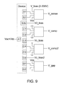
- FIG. 9 is an exemplary overall circuit diagram for the device of FIG. 3 .
- FIGS. 10A-E are exemplary device stack schematic drawings showing an embodiment of the fabrication of the MEMS metrology device in accordance with the embodiments of the present invention.
- FIG. 1 shows a device layout of a MEMS metrology device in accordance with an embodiment of the present invention.
- FIG. 2 is a detail view of the complementary measuring combs 102 of the device of FIG. 1 .
- FIG. 2 also shows the complementary comb-drive 104 that is used for increasing measurement sensitivity.
- capacitance changes across the measuring combs 102 correspond with the lateral translation of the shuttle 106 as it is actuated by the comb-drives (e.g., drives 108 and 110 ).
- 1 can be a compact device, fitting inside a 1 mm by 1 mm square or smaller, that can accurately measure in-plane over- or under-cut, effective Young's Modulus, and the comb-drive force for the material and process in which it is made.
- This device is useful for nanoscale calipers, manipulators, and force gauges, as well as for the scientific exploration of physical forces, developing fabrication processes, calibrating simulations of devices, and automatically recalibrating MEMS devices for environmental changes. Details of the complementary measuring combs 102 are shown in FIG. 2 .
- over- or under-cut refer to a deviation of a fabricated gap from its designed value.
- the procedure for measuring over- or under- cut, Young's Modulus, and the comb-drive force involves displacing the central cantilevered suspension 112 with the comb-drives 108 and 110 and measuring the deflection amount (x) with the complementary measuring combs 102 .
- two of the comb-drives 108 and 110 are actuated, which causes the cantilevers 112 to deflect and translate in the lateral direction 114 by deflection amount (x).
- Cantilevers 112 may act as springs that bias the shuttle 106 back to its original position after each displacement driven by the comb-drives.
- the over- or under-cut can be determined.
- they can be driven closer together with the secondary measuring comb drive 104 .
- the fringing field correction factor can be obtained for accurately determining the comb-drive force.
- the effective Young's Modulus of the system can be obtained.
- over- or under-cut varies as a function of beam width and beam gap, then the same measurements may be repeated for several different comb-drives each with varying beam width and gaps.
- FIGS. 2A-F show simplified drawings of the relative movement of the complementary measuring combs 102 and the varying capacitance vs. displacement for the combs 102 .
- FIGS. 2A-F show simplified drawings of the relative movement of the complementary measuring combs 102 and the varying capacitance vs. displacement for the combs 102 .
- FIGS. 2A-F show simplified drawings of the relative movement of the complementary measuring combs 102 and the varying capacitance vs. displacement for the combs 102 .
- FIGS. 2A-F show simplified drawings of the relative movement of the complementary measuring combs 102 and the varying capacitance vs. displacement for the combs 102 .
- FIGS. 2A-F show simplified drawings of the relative movement of the complementary measuring combs 102 and the varying capacitance vs. displacement for the combs 102 .
- the measuring combs 102 are used to find what applied voltages, V 1 and V 2 , on two separate comb drives 108 and 110 , will allow the cantilever 112 to displace by a fixed amount, (x).
- the comb drives 108 and 110 can have different gap sizes between comb fingers, g 1 and g 2 , and possibly different number of drive finger gaps, N 1 and N 2 .
- Multiple comb drives may be used to verify the over- or under-cut for beams and gaps of different sizes.
- one set of the complementary combs 102 can be offset (as shown in FIG. 2G ).
- the capacitance of one pair of combs can reach a maximum when the other pair (e.g., combs 102 - 1 ) reaches a minimum as the shuttle 106 is actuated. This allows a differential sense circuit to be used to measure the capacitance difference between the pair of complementary combs 102 - 1 and 102 - 2 .
- a design layout, circuits, and measurement steps used for characterizing over- or under-cut, effective Young's Modulus, and comb-drive forces using the MEMS metrology device in accordance with the embodiments of the present invention is described below.
- the components of the characterization device are labeled in Design Layout section.
- the measurement circuit and set-up are shown in the Circuit Layout section.
- the measurement procedures are shown in Measurements section.
- FIG. 3 shows an exemplary schematic diagram of an embodiment of the device of FIG. 1 .
- electrical terminals are shown as cross-hatched boxes (e.g., terminals A 1 , S 1 , and S 2 of FIG. 3 ).
- the design includes the following components or subsystems:
- the width of the guided suspension 112 , cw can be chosen as small as possible to keep the required length of the guided suspension, cl, as low as possible.
- the second structure should contain another guided suspension of a different width, a good value may be cw*1.25 (this doubles the stiffness) but the optimal value may depend on the process.
- the length of the guided suspension 112 , cl should be chosen small enough that processing steps will not break it, stiction will not immobilize it, and it will fit in the desired amount of space.
- cl should be chosen large enough that the shuttle 106 may move far enough (without breaking the suspension) that the measuring combs 102 senses a capacitive peak. Also, cl should be chosen large enough that the required voltage to achieve the desired displacement (x) of the shuttle 106 is kept small enough for the equipment to handle. The shuttle 106 should be kept as stiff as possible while still being releasable. For improved sensitivity and simplicity, driving and sensing comb-drives (e.g., drives 108 / 110 ) should be matched on both sides of the shuttle 106 . When measuring cut-errors for many different geometries, it may be more economical to use differing comb-drive dimensions for comb-drives located on opposite sides.
- FIG. 4 shows an exemplary schematic diagram of one embodiment of the measuring combs 102 of FIG. 3 .
- Vertical members 102 a in FIG. 4 correspond with the vertical members 102 a of FIG. 3 .
- Electrical terminals C 1 and C 2 are located adjacent anchors 410 and 420 , respectively.
- Terminal C 3 is located within comb drive 104 .
- the design of the measuring combs 102 includes the following:
- the following guidelines can be used in the overall design of the device of FIG. 4 .
- the set of matched teeth 102 - 1 and mismatched teeth 102 - 2 should have the same spacing between comb teeth.
- the suspension drive 104 may be joined or separated depending on whether more simplicity or flexibility is needed.
- FIG. 5 shows an exemplary schematic diagram of a second embodiment of a measuring combs 102 of FIG. 3 .
- four teeth sets, 502 - 1 , - 2 , - 3 , and - 4 may be used having four different alignments, the alignment of each set shifted by a quarter of the distance between adjacent comb teeth.
- the sinusoidal-like capacitance function is then shifted by 90 degrees, and a Hariharan type algorithm may be applied to find the displacement (x) (described in the measurements section below).
- FIG. 6 shows an exemplary schematic diagram of an embodiment of the gap closing sense array 302 of FIG. 3 .
- An optional gap-closing sense array 302 may be used to further refine the measurements of cut-error and also measure layer thickness.
- Each gap-closing sensor has two fixed gaps 601 and 602 , each defined between a beam of the gap sensor and a beam carried on the shuttle 106 .
- beam 604 of the gap sensor overlaps with beam 606 of the shuttle by a set distance.
- the second set of beams 603 and 605 overlap by an additional distance, dw, compared to the overlap distance between beams 604 and 606 .
- the differential capacitance between the two sets of beams 604 / 606 and 603 / 605 can be used to determine the value of gaps 601 and 602 , and therefore cut-error, the method of which is discussed in further detail below.
- G 1 and G 2 can be tied to A 1 if gap-closing sensing is not used (to avoid charging effects). In general, A 1 's DC offset (if used) should also be applied to G 1 and G 2 .
- FIG. 7 shown an exemplary schematic diagram of the drive/sense comb drives (e.g., such as drives 108 / 110 ) of FIG. 3 .
- comb-drives 702 / 703 / 704 / 705 are disposed on both sides of shuttle 106 , one of which may be driven while the differential capacitance is sensed between them by combs 102 (not shown).
- Each comb-drive e.g., 702 and 703
- Each comb-drive may have different finger widths, w, and gap spacings, g, between fingers. The finger overlap can be kept small to reduce levitation effects.
- Comb-drives 704 and 705 on the opposite side of the shuttle 106 may have fewer comb-fingers but more overlap to reduce tilt, or may be identical to the opposing comb-drives 702 and 703 , respectively.
- FIG. 8 shows an exemplary circuit diagram of the differential sense portion of the device of FIG. 3 , and which does not include capacitive bypassing of the power supply.
- sensitive differential capacitance measurements (with a resolution around or below 10 aF) are made while a voltage sweep is supplied to the driving comb-set.
- resistor values are denoted with an “R” and capacitor values are denoted with a “C”.
- the signal from the DC biasing (Vb 1 and Vb 2 ) is low-pass filtered through resistor, R 1 , and capacitor, C 1 (large).
- C 2 is set to a small capacitive value and R 2 is set to a large resistive value.
- ) is roughly 2*d/C 2 .
- C 2 is not used, and R 2 is set to around a 100 Kohm level.
- ) is roughly 2*d*R 2 *omega (where omega is the frequency of Vac).
- the second stage amplifier can further be used to amplify the signal.
- the gain is roughly R 4 /R 3 .
- the alternating signal can be converted to a DC signal through an RMS to DC converter.
- FIG. 9 shows an exemplary overall circuit diagram for the device of FIG. 3 .
- Terminals not shown are grounded.
- Vac is an alternating signal (>200 kHz) applied to the suspension and
- Vdc is a bias applied to the suspension (and other components) to correct for the levitation effect.
- Step A The differential sense circuit shown in FIG. 8 is calibrated so that the capacitance, d, is known from a measurement of V (note that there is a factor of 2).
- An LCR meter such as an HP4824A may be used for this purpose.
- Step B The suspension sweeping V_bias is moved and V_comp as well as V_sense (*) are measured.
- the V_bias and V_sense values associated with the first peak of V_comp are found (it can be more accurate to do this measurement by curve-fitting). Corrections can be made when the output is shifted (due to imperfectly matched capacitances).
- the values for V_comp may be shifted such that the max and min are equidistant from the origin.
- Vc_bias is adjusted until the maxima and minima are known to the desired accuracy.
- the shuttle moves a distance of half the distance (x) between successive complementary-comb teeth.
- the change of capacitance (dC) can then be determined from the calibration data and V_sense.
- the force (F) exerted on the suspension is then V_bias 2 dC/(2*x).
- Step C By using a model of the comb-drive force (F) allows the determination of the cut error (e) from two different comb-drive sets.
- V_bias bias voltages V 1 and V 2 , are found for the two sets that generate the same force (same displacement). Cut error is then computed as
- Step D The effective Young's Modulus may be computed as
- E F ⁇ ( l + e ) 3 2 ⁇ ⁇ x ⁇ ⁇ h ⁇ ( w - e ) 3 where 1 is the cantilever length, and w is the cantilever width.
- the optional comb-sets (B in FIG. 7 ) can be used. For each biasing voltage, V_bias, the following steps are taken to remove levitation effects.
- the cut error for differing geometries can also be measured using a gap-closing actuator shown in FIG. 6 .
- This arrangement can provide for more accuracy.
- the measurement includes the following steps:
- V_comp and V_comp 2 will be 2 periodic functions (of displacement which is proportional to V_bias 2 ). They will also be 90 degrees out of phase with one another. The minima and maxima can be found when the function atan(V_comp 2 /V_comp) crosses multiples of pi. Near these regions, the data can be linearly fit to determine this crossing value precisely. Note that the atan function must be unwrapped (when values cross pi, they jump to ⁇ pi) and at that point, 2*pi is added to the results to make them continuous).
- the MEMS metrology device in accordance with the embodiments of the present invention can be fabricated using a silicon-on-insulator substrate from a single mask, as shown in FIGS. 10A-E .
- the fabrication process includes the following steps.
- the fabrication of the device starts with a handling layer 1002 that has disposed on it an oxide layer 1004 that in turn has a device layer 1006 disposed on it ( FIG. 10A ).
- a photoresist layer 1008 is deposited on the device layer 1006 ( FIG. 10B ).
- the photoresist layer 1008 is patterned ( FIG. 10C ).
- the device layer 1006 and the oxide layer 1004 are etched ( FIG.
- the device shown in FIG. 1 is approximately 25-50 ⁇ m thick, has a foot print of approximately 1.5 mm by 1.0 mm, or preferably less than 1.0 mm by 1.0 mm.
- the MEMS metrology device in accordance with the embodiments of the present invention can be fabricated during the same fabrication process and formed adjacent to the MEMS device which will be monitored by the metrology device. The metrology device can then be used to measure both the under or over-cut of the device and also monitor its material, process, geometry and dynamic properties of MEMS device.
- Prototype MEMS metrology devices have been demonstrated to be inexpensive, reliable and accurate, having resolutions better than or similar to the resolution of optical microscopy device and nearing SEM device resolutions. Furthermore, due to the symmetric nature of over- or under-cut the deflection measurements of the MEMS metrology devices are resilient to the variation of comb tips. Such comb-tip variations include variations due to cut error resulting in narrower or wider combs; variations due to the filleting where combs are shortened and rounded; and cross-sectional variations.
Abstract
Description
e=(N 1 V 1 2 g 2 −N 2 V 2 2 g 1)/(N 1 V 1 2 −N 2 V 2 2).
e=(S 2 N 1 g 2 −N 2 g 1)/(S 2 N 1 −N 2).
a=C(g 1 −e)/(xN 1ε0εair h), where (h) is the thickness of the silicon.
Next for a uniform over- or under-cut, the effective Young's Modulus, (E), of the silicon is found by:
E=CV 1 2(L−e)3/(4x 2 h(w+e)3),
-
- A. an anchored guided
suspension 112 with cantilever width, cw, and cantilever length, cl, - B. a
shuttle 106 that joins thesuspension 112 and the driving and sensing apparatus, - C. a set of driving and sensing comb-
drives 108/110, - D. measuring combs 102 to sense displacement of the
shuttle 106, and - E. an optional gap-
closing sense array 302 for further assessing cut-error.
- A. an anchored guided
-
- F. one set of matched teeth 102-1,
- G. one set of mismatched teeth 102-2,
-
H. suspensions 402 that allow the teeth sets to be moved towards each other by movingcombs 102 b, and - I. comb-
drive 104 to actuate thesuspensions 402.
where 1 is the cantilever length, and w is the cantilever width.
-
- A. Apply bias to V2_bias until |V_comp| is maximized.
- B. Apply bias to Vdc until |V_comp| is maximized.
-
- A. As V_bias is swept, measure V_gap.
- B. Use the calibration data to convert V_gap to capacitance, C_gap.
- C. Use the complementary-comb data to convert V_bias to the translation, x.
- D. Fit the data to C_gap=αε0εairA/(gmodel−x). (αε0εairA is constant)
- E. Cut error is then gmodel−g.
- F. A short set (3-5 microns in length) of gap-closing sensors may be used as gap stops to allow the determination of the sidewall angle. The cut-error determined in step E is near the midpoint of the layer. Actuate the shuttle until the gap is reached. Measure the displacement, gbottom, using the V_sense data. The sidewall angle is approximately (gbottom−gmodel)/(h/2).
- G. Similarly, as the gap is closed, the fringing-field effect is reduced. At the point where the fringing-field effect is sufficiently reduced, the layer thickness, h, may be measured by finding the area A (from step D) and dividing by the layout protruding length (it is not affected by cut error).
Claims (20)
Priority Applications (1)
| Application Number | Priority Date | Filing Date | Title |
|---|---|---|---|
| US11/737,532 US8079246B2 (en) | 2006-04-19 | 2007-04-19 | Integrated MEMS metrology device using complementary measuring combs |
Applications Claiming Priority (2)
| Application Number | Priority Date | Filing Date | Title |
|---|---|---|---|
| US79342406P | 2006-04-19 | 2006-04-19 | |
| US11/737,532 US8079246B2 (en) | 2006-04-19 | 2007-04-19 | Integrated MEMS metrology device using complementary measuring combs |
Publications (2)
| Publication Number | Publication Date |
|---|---|
| US20090322365A1 US20090322365A1 (en) | 2009-12-31 |
| US8079246B2 true US8079246B2 (en) | 2011-12-20 |
Family
ID=38625734
Family Applications (1)
| Application Number | Title | Priority Date | Filing Date |
|---|---|---|---|
| US11/737,532 Expired - Fee Related US8079246B2 (en) | 2006-04-19 | 2007-04-19 | Integrated MEMS metrology device using complementary measuring combs |
Country Status (2)
| Country | Link |
|---|---|
| US (1) | US8079246B2 (en) |
| WO (1) | WO2007124357A2 (en) |
Cited By (6)
| Publication number | Priority date | Publication date | Assignee | Title |
|---|---|---|---|---|
| US8861752B2 (en) | 2011-08-16 | 2014-10-14 | Empire Technology Development Llc | Techniques for generating audio signals |
| US20150177272A1 (en) * | 2012-06-13 | 2015-06-25 | Purdue Research Foundation | Microelectromechanical system and methods of use |
| US9913048B2 (en) | 2014-02-08 | 2018-03-06 | Empire Technology Development Llc | MEMS-based audio speaker system with modulation element |
| US10123126B2 (en) | 2014-02-08 | 2018-11-06 | Empire Technology Development Llc | MEMS-based audio speaker system using single sideband modulation |
| US10271146B2 (en) | 2014-02-08 | 2019-04-23 | Empire Technology Development Llc | MEMS dual comb drive |
| US10284961B2 (en) * | 2014-02-08 | 2019-05-07 | Empire Technology Development Llc | MEMS-based structure for pico speaker |
Families Citing this family (8)
| Publication number | Priority date | Publication date | Assignee | Title |
|---|---|---|---|---|
| US20090051369A1 (en) * | 2007-08-21 | 2009-02-26 | Qualcomm Incorporated | System and method for measuring adhesion forces in mems devices |
| KR20100121498A (en) | 2008-02-11 | 2010-11-17 | 퀄컴 엠이엠스 테크놀로지스, 인크. | Method and apparatus for sensing, measurement or characterization of display elements integrated with the display drive scheme, and system and applications using the same |
| US8258800B2 (en) | 2008-02-11 | 2012-09-04 | Qualcomm Mems Technologies, Inc. | Methods for measurement and characterization of interferometric modulators |
| WO2009102581A1 (en) | 2008-02-11 | 2009-08-20 | Qualcomm Mems Technologies, Inc. | Impedance sensing to determine pixel state in a passively addressed display array |
| WO2009134501A2 (en) * | 2008-02-11 | 2009-11-05 | Qualcomm Mems Technologies, Inc. | Methods for measurement and characterization of interferometric modulators |
| EP2960637B1 (en) * | 2014-06-24 | 2019-08-28 | Femtotools AG | Design and interface of a microfabricated scanning force sensor for combined force and position sensing |
| CN104370272B (en) * | 2014-10-30 | 2016-07-06 | 无锡微奥科技有限公司 | A kind of MEMS autoregistration height comb and manufacture method thereof |
| EP3718960B1 (en) | 2014-12-10 | 2023-10-25 | Paul D. Okulov | Structural health and usage monitoring system |
Citations (2)
| Publication number | Priority date | Publication date | Assignee | Title |
|---|---|---|---|---|
| US20040113647A1 (en) * | 2002-09-18 | 2004-06-17 | Nilmoni Deb | Built-in self test of MEMS |
| US7573022B2 (en) * | 2005-07-27 | 2009-08-11 | The Regents Of The University Of California | Method for fabricating vertically-offset interdigitated comb actuator device |
-
2007
- 2007-04-19 WO PCT/US2007/066963 patent/WO2007124357A2/en active Application Filing
- 2007-04-19 US US11/737,532 patent/US8079246B2/en not_active Expired - Fee Related
Patent Citations (3)
| Publication number | Priority date | Publication date | Assignee | Title |
|---|---|---|---|---|
| US20040113647A1 (en) * | 2002-09-18 | 2004-06-17 | Nilmoni Deb | Built-in self test of MEMS |
| US7152474B2 (en) * | 2002-09-18 | 2006-12-26 | Carnegie Mellon University | Built-in self test of MEMS |
| US7573022B2 (en) * | 2005-07-27 | 2009-08-11 | The Regents Of The University Of California | Method for fabricating vertically-offset interdigitated comb actuator device |
Cited By (8)
| Publication number | Priority date | Publication date | Assignee | Title |
|---|---|---|---|---|
| US8861752B2 (en) | 2011-08-16 | 2014-10-14 | Empire Technology Development Llc | Techniques for generating audio signals |
| US9866948B2 (en) | 2011-08-16 | 2018-01-09 | Empire Technology Development Llc | Techniques for generating audio signals |
| US10448146B2 (en) | 2011-08-16 | 2019-10-15 | Empire Technology Development Llc | Techniques for generating audio signals |
| US20150177272A1 (en) * | 2012-06-13 | 2015-06-25 | Purdue Research Foundation | Microelectromechanical system and methods of use |
| US9913048B2 (en) | 2014-02-08 | 2018-03-06 | Empire Technology Development Llc | MEMS-based audio speaker system with modulation element |
| US10123126B2 (en) | 2014-02-08 | 2018-11-06 | Empire Technology Development Llc | MEMS-based audio speaker system using single sideband modulation |
| US10271146B2 (en) | 2014-02-08 | 2019-04-23 | Empire Technology Development Llc | MEMS dual comb drive |
| US10284961B2 (en) * | 2014-02-08 | 2019-05-07 | Empire Technology Development Llc | MEMS-based structure for pico speaker |
Also Published As
| Publication number | Publication date |
|---|---|
| WO2007124357A9 (en) | 2008-07-31 |
| WO2007124357A2 (en) | 2007-11-01 |
| US20090322365A1 (en) | 2009-12-31 |
| WO2007124357A3 (en) | 2008-12-11 |
Similar Documents
| Publication | Publication Date | Title |
|---|---|---|
| US8079246B2 (en) | Integrated MEMS metrology device using complementary measuring combs | |
| US8461833B2 (en) | Method for determining the sensitivity of an acceleration sensor or magnetic field sensor | |
| EP1763675B1 (en) | Method for calibrating accelerometer sensitivity | |
| US6545495B2 (en) | Method and apparatus for self-calibration of capacitive sensors | |
| EP0543901B1 (en) | Monolithic accelerometer | |
| KR100513346B1 (en) | A capacitance accelerometer having a compensation elctrode | |
| EP2336788B1 (en) | Inertial sensor | |
| Miller et al. | Microelectromechanical scanning probe instruments for array architectures | |
| KR100379206B1 (en) | Capacitance-type external-force detecting device with improved sensitivity | |
| CN107003333B9 (en) | MEMS sensor and semiconductor package | |
| US20090158847A1 (en) | Angular Velocity Sensor | |
| CN110567494B (en) | Capacitive position sensing for capacitively driven MEMS devices | |
| US7598746B2 (en) | Surface voltmeter and surface voltage measurement method | |
| JP2004510984A (en) | Method and apparatus for electrical zeroing for micromechanical components | |
| US8833135B2 (en) | Sensor system and method for calibrating a sensor system | |
| JP2001330621A (en) | Method for manufacturing semiconductor dynamic quantity sensor | |
| JP5193541B2 (en) | Angular velocity detector | |
| Rocha et al. | Auto-calibrated capacitive MEMS accelerometer | |
| Chang et al. | Simulation and characterization of a CMOS-MEMS gyroscope with parasitic-insensitive sensing | |
| Mol et al. | Read-out calibration of a SOI capacitive transducer using the pull-in voltage | |
| JP2010185798A (en) | Capacitance sensor | |
| Li et al. | Improved modeling of the comb drive levitation effect by using Schwartz-Christoffel mapping | |
| KR19980041111A (en) | External force sensing device | |
| deBoer et al. | Micromachine friction test apparatus | |
| Clark | Post-Packaged Measurement of MEMS Gap, Displacement, Force, Stiffness, Mass, Damping, and Quality Factor |
Legal Events
| Date | Code | Title | Description |
|---|---|---|---|
| AS | Assignment |
Owner name: THE REGENTS OF THE UNIVERSITY OF CALIFORNIA, CALIF Free format text: ASSIGNMENT OF ASSIGNORS INTEREST;ASSIGNORS:GARMIRE, DAVID;CHOO, HYUCK;MULLER, RICHARD S.;AND OTHERS;REEL/FRAME:019525/0435;SIGNING DATES FROM 20070620 TO 20070702 Owner name: THE REGENTS OF THE UNIVERSITY OF CALIFORNIA, CALIF Free format text: ASSIGNMENT OF ASSIGNORS INTEREST;ASSIGNORS:GARMIRE, DAVID;CHOO, HYUCK;MULLER, RICHARD S.;AND OTHERS;SIGNING DATES FROM 20070620 TO 20070702;REEL/FRAME:019525/0435 |
|
| AS | Assignment |
Owner name: CALIFORNIA BERKELEY, UNIVERSITY OF, CALIFORNIA Free format text: CONFIRMATORY LICENSE;ASSIGNOR:NATIONAL SCIENCE FOUNDATION;REEL/FRAME:020158/0834 Effective date: 20071025 |
|
| STCF | Information on status: patent grant |
Free format text: PATENTED CASE |
|
| FEPP | Fee payment procedure |
Free format text: PAYOR NUMBER ASSIGNED (ORIGINAL EVENT CODE: ASPN); ENTITY STATUS OF PATENT OWNER: SMALL ENTITY |
|
| FPAY | Fee payment |
Year of fee payment: 4 |
|
| FEPP | Fee payment procedure |
Free format text: MAINTENANCE FEE REMINDER MAILED (ORIGINAL EVENT CODE: REM.); ENTITY STATUS OF PATENT OWNER: SMALL ENTITY |
|
| LAPS | Lapse for failure to pay maintenance fees |
Free format text: PATENT EXPIRED FOR FAILURE TO PAY MAINTENANCE FEES (ORIGINAL EVENT CODE: EXP.); ENTITY STATUS OF PATENT OWNER: SMALL ENTITY |
|
| STCH | Information on status: patent discontinuation |
Free format text: PATENT EXPIRED DUE TO NONPAYMENT OF MAINTENANCE FEES UNDER 37 CFR 1.362 |
|
| FP | Lapsed due to failure to pay maintenance fee |
Effective date: 20191220 |