US8077171B2 - Signal regulator module and related display device - Google Patents
Signal regulator module and related display device Download PDFInfo
- Publication number
- US8077171B2 US8077171B2 US11/853,022 US85302207A US8077171B2 US 8077171 B2 US8077171 B2 US 8077171B2 US 85302207 A US85302207 A US 85302207A US 8077171 B2 US8077171 B2 US 8077171B2
- Authority
- US
- United States
- Prior art keywords
- signal
- electrically coupled
- driving
- averaging
- circuit
- Prior art date
- Legal status (The legal status is an assumption and is not a legal conclusion. Google has not performed a legal analysis and makes no representation as to the accuracy of the status listed.)
- Active, expires
Links
Images


Classifications
-
- H—ELECTRICITY
- H05—ELECTRIC TECHNIQUES NOT OTHERWISE PROVIDED FOR
- H05B—ELECTRIC HEATING; ELECTRIC LIGHT SOURCES NOT OTHERWISE PROVIDED FOR; CIRCUIT ARRANGEMENTS FOR ELECTRIC LIGHT SOURCES, IN GENERAL
- H05B41/00—Circuit arrangements or apparatus for igniting or operating discharge lamps
- H05B41/14—Circuit arrangements
- H05B41/26—Circuit arrangements in which the lamp is fed by power derived from dc by means of a converter, e.g. by high-voltage dc
- H05B41/28—Circuit arrangements in which the lamp is fed by power derived from dc by means of a converter, e.g. by high-voltage dc using static converters
- H05B41/282—Circuit arrangements in which the lamp is fed by power derived from dc by means of a converter, e.g. by high-voltage dc using static converters with semiconductor devices
- H05B41/2821—Circuit arrangements in which the lamp is fed by power derived from dc by means of a converter, e.g. by high-voltage dc using static converters with semiconductor devices by means of a single-switch converter or a parallel push-pull converter in the final stage
- H05B41/2824—Circuit arrangements in which the lamp is fed by power derived from dc by means of a converter, e.g. by high-voltage dc using static converters with semiconductor devices by means of a single-switch converter or a parallel push-pull converter in the final stage using control circuits for the switching element
-
- G—PHYSICS
- G09—EDUCATION; CRYPTOGRAPHY; DISPLAY; ADVERTISING; SEALS
- G09G—ARRANGEMENTS OR CIRCUITS FOR CONTROL OF INDICATING DEVICES USING STATIC MEANS TO PRESENT VARIABLE INFORMATION
- G09G2320/00—Control of display operating conditions
- G09G2320/06—Adjustment of display parameters
- G09G2320/0606—Manual adjustment
-
- G—PHYSICS
- G09—EDUCATION; CRYPTOGRAPHY; DISPLAY; ADVERTISING; SEALS
- G09G—ARRANGEMENTS OR CIRCUITS FOR CONTROL OF INDICATING DEVICES USING STATIC MEANS TO PRESENT VARIABLE INFORMATION
- G09G2320/00—Control of display operating conditions
- G09G2320/06—Adjustment of display parameters
- G09G2320/0626—Adjustment of display parameters for control of overall brightness
- G09G2320/0633—Adjustment of display parameters for control of overall brightness by amplitude modulation of the brightness of the illumination source
-
- G—PHYSICS
- G09—EDUCATION; CRYPTOGRAPHY; DISPLAY; ADVERTISING; SEALS
- G09G—ARRANGEMENTS OR CIRCUITS FOR CONTROL OF INDICATING DEVICES USING STATIC MEANS TO PRESENT VARIABLE INFORMATION
- G09G3/00—Control arrangements or circuits, of interest only in connection with visual indicators other than cathode-ray tubes
- G09G3/20—Control arrangements or circuits, of interest only in connection with visual indicators other than cathode-ray tubes for presentation of an assembly of a number of characters, e.g. a page, by composing the assembly by combination of individual elements arranged in a matrix no fixed position being assigned to or needed to be assigned to the individual characters or partial characters
- G09G3/34—Control arrangements or circuits, of interest only in connection with visual indicators other than cathode-ray tubes for presentation of an assembly of a number of characters, e.g. a page, by composing the assembly by combination of individual elements arranged in a matrix no fixed position being assigned to or needed to be assigned to the individual characters or partial characters by control of light from an independent source
- G09G3/3406—Control of illumination source
-
- Y—GENERAL TAGGING OF NEW TECHNOLOGICAL DEVELOPMENTS; GENERAL TAGGING OF CROSS-SECTIONAL TECHNOLOGIES SPANNING OVER SEVERAL SECTIONS OF THE IPC; TECHNICAL SUBJECTS COVERED BY FORMER USPC CROSS-REFERENCE ART COLLECTIONS [XRACs] AND DIGESTS
- Y02—TECHNOLOGIES OR APPLICATIONS FOR MITIGATION OR ADAPTATION AGAINST CLIMATE CHANGE
- Y02B—CLIMATE CHANGE MITIGATION TECHNOLOGIES RELATED TO BUILDINGS, e.g. HOUSING, HOUSE APPLIANCES OR RELATED END-USER APPLICATIONS
- Y02B20/00—Energy efficient lighting technologies, e.g. halogen lamps or gas discharge lamps
Definitions
- the present invention relates to a signal regulator module, and more particularly, to a signal regulator module capable of adjusting driving signals outputted by a driving circuit to light sources of a display panel.
- a liquid crystal display (LCD) device can provide rich images by controlling liquid crystal pixels of a display panel using transistors arranged in matrix, together with appropriate electronic components such as capacitors, switches, and pads. Due to thin appearances, low power consumption, and low radiation, LCD devices have gradually replaced traditional cathode ray tube (CRT) displays and are widely used in portable electronic devices such as notebook computers, personal digital assistants (PDA) and digital cameras.
- CTR cathode ray tube
- an LCD device includes an LCD panel and a backlight module disposed at the lower or lateral sides of the LCD panel.
- a light source and various optical devices are used for providing high-intensity and uniform light for the LCD panel.
- the LCD device can display corresponding images.
- the backlight module including a light source and an optical film, is capable of providing uniform light.
- backlight modules can be categorized into direct-type and edge-type backlight modules. In a direct-type backlight module, light is generated directly beneath the LCD panel. In an edge-type backlight module, light is generated near the lateral sides of the LCD panel. Since light of higher-intensity is provided when generated directly beneath the LCD panel, the direct-type backlight module can be applied in high-brightness or large-size LCD panels, such as in flat panel television sets.
- FIG. 1 is a diagram of a prior art LCD backlight module driving circuit 10 .
- the LCD backlight module driving circuit 10 includes a plurality of transformers TR 1 -TRn for respectively driving lamps L 1 -Ln.
- each lamp is driven by a transformer.
- the panel size becomes larger and the number of lamps used in the LCD device also increases accordingly. Therefore, the prior art LCD backlight module driving circuit 10 requires more transformers, which largely raises manufacturing costs.
- FIG. 2 is a diagram of another prior art LCD backlight module driving circuit 20 .
- the LCD backlight module driving circuit 20 includes a transformer TR for simultaneously driving lamps L 1 -Ln.
- I L1 -I Ln represent the currents passing through the lamps L 1 -Ln, respectively.
- a transformer is used for driving multiple lamps. Therefore, in large-size applications, the number of the transformers and driving switches can be reduced, thereby cutting manufacturing costs.
- the lamps L 1 -Ln may have different characteristics, the currents I L1 -I Ln passing through the lamps L 1 -Ln may also vary. Each lamp can thus provide distinct luminance, which lowers the uniformity of the backlight module and influences the display quality of the LCD device.
- FIG. 3 is a diagram of another prior art LCD backlight module driving circuit 30 .
- a balance circuit is used for improving the current uniformity when driving multiple lamps, and only two lamps are depicted in FIG. 3 for ease of illustration.
- the LCD backlight module driving circuit 30 includes a transformer TR and a balance circuit 32 for driving lamps L 1 and L 2 .
- I L1 and I L2 represent the currents passing through the lamps L 1 and L 2 , respectively.
- the balance circuit 32 includes active components such as transistors Qp and Qn, diodes Dp and Dn, comparator 34 , and impedance device Cx.
- the balance circuit 32 Since the balance circuit 32 adopts an active design, it generates a feedback signal V 1 pertaining to the current I L1 and a feedback signal V 2 pertaining to the current I L2 .
- the comparator 34 can compare the feedback signals V 1 and V 2 , output a corresponding switch voltage signal Vsw based on the difference between the feedback signals V 1 and V 2 , and send the switch voltage signal Vsw to the gates of the transistors Qp and Qn. In response to the switch voltage signal Vsw, the transistors Qp and Qn are turned on and turned off for regulating the current I L2 , so that the current I L2 can approach the current I L1 .
- the comparator 34 merely capable of outputting logic signals having high/low levels, cannot reveal the accurate difference between the currents I L1 and I L2 . Due to slow response speed of the comparator 34 , it takes a long time for the LCD backlight module driving circuit 30 to reach equilibrium. Also, since the balance circuit 32 can only be used at the low-voltage end of the lamps, the LCD backlight module driving circuit 30 cannot be applied to large-size panels having a dual-side driving structure.
- the present invention provides a signal regulator module for adjusting driving signals outputted by a driving circuit to light sources of a display panel comprising a first floating current regulator electrically coupled to the driving circuit and a first light source of the display panel for regulating a first driving signal outputted by the driving circuit to the first light source, adjusting the first driving signal based on a first feedback signal in a photo couple means, and outputting the adjusted first driving signal; a first signal sensor electrically coupled to the first floating current regulator for generating a corresponding first voltage signal based on the first driving signal in a photo couple means; and a feedback controller electrically coupled to the first signal sensor and the first floating current regulator for generating the first feedback signal based on the first voltage signal and outputting the first feedback signal to the first floating current regulator.
- the present invention also provides a display device capable of adjusting driving signals comprising a light generating means for providing light in response to a driving signal; a driving means for generating the driving signal; and a signal adjusting means for generating a corresponding feedback signal by sensing the driving signal through a photo couple means, adjusting the driving signal in response to the feedback signal, and outputting the adjusted driving signal to the light generating means.
- FIG. 1 is a diagram of a prior art LCD backlight module driving circuit.
- FIG. 2 is a diagram of another prior art LCD backlight module driving circuit.
- FIG. 3 is a diagram of another prior art LCD backlight module driving circuit.
- FIG. 4 is a diagram of an LCD backlight module according to the present invention.
- FIG. 5 is a diagram of an LCD backlight module according to the present invention.
- FIG. 6 is a diagram of a signal regulator module according to a first embodiment of the present invention.
- FIG. 7 is a diagram of a signal regulator module according to a second embodiment of the present invention.
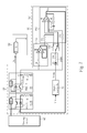
- FIG. 4 is a diagram of an LCD backlight module 40 according to one embodiment of the present invention.
- the LCD backlight module 40 including a driving circuit 42 , a signal regulator module 60 and a digital controller 70 , can drive a lamp module 52 having a single lamp or a plurality of lamps.
- lamps L 1 -Ln are used for illustrating the embodiment, and I L1 -I Ln respectively represent the currents passing through the lamps L 1 -Ln.
- the driving circuit 42 includes a single driver 44 , a single transformer 46 and a control chip 48 .
- the single driver 44 can transform an input DC voltage into an alternative current (AC) voltage.
- the single transformer can then enhance the AC voltage for providing appropriate voltages for the lamp module 52 .
- the control chip 48 can provide control signals required for operating the LCD backlight module 40 .
- the signal regulator module 60 includes floating current regulators FCR 1 -FCRn, signal sensors SS 1 -SSn, and a feedback controller 62 .
- the signal regulator module 60 detects the currents I L1 -I Ln passing through the lamps L 1 -Ln respectively using the signal sensors SS 1 -SSn, and then sends feedback signals V fb1 -V fbn respectively to the floating current regulators FCR 1 -FCRn using the feedback controller 62 .
- the floating current regulators FCR 1 -FCRn can then adjust the values of the currents I L1 -I Ln respectively based on the feedback signals V fb1 -V fbn on a real time basis.
- the signal regulator module 60 adopts an active design and can perform real-time current regulation based on the actual current passing through each lamp. Each lamp can thus provide current of the nominal value.
- the signal regulator module 60 and the driving circuit 42 can be disposed on the same printed circuited board (PCB), or separately on two different PCBs.
- the signal regulator module 60 can include an integral-type integrated circuit manufactured in a high-pressure process, or a current regulating circuit having circuit devices. The detailed structure of the signal regulator module 60 will be described in the following paragraphs.
- the digital controller 70 can achieve image processing by performing various timing and brightness controls on a single lamp or on all lamps of the backlight module.
- the digital controller 70 receives and processes a control signal V IN sent by the system for image processing, and then outputs signals V COM1 -V COMn respectively corresponding to the lamps L 1 -Ln for controlling the luminance of the lamps on a real time basis. By providing the most appropriate light intensity, display images can have a better visual performance in contrast and brightness. If the LCD backlight module 40 does not receive the control signal V IN for image processing, the digital controller 70 operates based on its default settings. Under these circumstances, the LCD backlight module 40 performs current regulation via the signal regulator module 60 , thereby equalizing the current passing through each lamp.
- the LCD backlight module 40 If the LCD backlight module 40 receives the control signal V IN for image processing, the LCD backlight module 40 first performs current regulation via the signal regulator module 60 , thereby equalizing the current passing through each lamp. Next, the digital controller 70 outputs the signals V COM1 -V COMn based on the control signal V IN . Image processing can be achieved by controlling the brightness of each lamp. Therefore, the LCD backlight module 40 can provide current regulation and image processing simultaneously.
- FIG. 5 for a diagram of another LCD backlight module 50 according to the present invention.
- the LCD backlight module 50 also including a driving circuit 42 , a signal regulator module 60 and a digital controller 70 , can drive the lamp module 52 .
- the LCD backlight module 50 differs from the LCD backlight module 40 in that the signal regulator module 60 of the LCD backlight module 40 is electrically coupled between the driving circuit 42 and the high-voltage terminal of the lamp module 52 , while the signal regulator module 60 of the LCD backlight module 50 is electrically coupled between the low-voltage terminal of the lamp module 52 and ground. Since the signal regulator module 60 of the present invention adopts a floating-type design, high voltages and low voltages are isolated in a photo couple means.
- the signal regulator 60 can be disposed at the high-voltage terminal of the lamp module 52 , as illustrated by the LCD backlight module 40 in FIG. 4 .
- the signal regulator 60 can also be disposed at the low-voltage terminal of the lamp module 52 , as illustrated by the LCD backlight module 50 in FIG. 5 .
- FIG. 6 a diagram of the signal regulator module 60 according to a first embodiment of the present invention.
- the lamp module 52 includes two lamps L 1 and L 2 .
- I L1 and I L2 represent the currents passing through the lamps L 1 and L 2 , respectively.
- the signal regulator module 60 includes floating current regulators FCR 1 and FCR 2 , signal sensors SS 1 and SS 2 , and a feedback controller 62 .
- each of the floating current regulators and the signal sensors includes photo couple devices, impedance devices and resistors.
- the photo couple device PHC 12 of the signal sensor SS 1 and the photo couple device PHC 22 of the signal sensor SS 2 can respectively detect the currents I L1 and I L2 passing through the lamps L 1 and L 2 .
- Larger currents I L1 and I L2 induce larger currents passing through the internal photodiodes of the photo couple devices and lengthen the conducting time of the internal phototransistors of the photo couple devices, thereby resulting in larger internal currents I PHC1 and I PHC2 .
- the current signals I PHC1 and I PHC2 are transformed into voltage signals V 1 and V 2 via the resistors R 12 and R 22 , respectively. Consequently, as the currents I L1 and I L2 increase, the voltage signals V 1 and V 2 become larger accordingly; as the currents I L1 and I L2 decrease, the voltage signals V 1 and V 2 become smaller accordingly.
- the feedback controller 62 includes an averaging circuit 72 , dimmers DIM 1 and DIM 2 , and proportional integral controllers (PI controllers) PIC 1 and PIC 2 .
- the averaging circuit 72 electrically coupled to the signal sensors SS 1 and SS 2 , can generate an averaging signal V AVG as the reference voltage for the PI controllers PIC 1 and PIC 2 when performing a closed-loop feedback control. Due to characteristic variances between different lamps, each lamp provides a distinct current when illuminating. In the first embodiment of the present invention, the averaging circuit 72 can generate an average value of all lamp currents.
- the averaging circuit 72 including an operational amplifier OP and a resistor R, can achieve signal isolation and prevent the misoperations of the averaging circuit 72 due to loading effects.
- the operation of the averaging circuit 72 can be represented by the following formula:
- V 1 - V AVG R V AVG - V 2 R + V AVG - V 3 R + V AVG - V 4 R + ... + V AVG - V n R
- V AVG V 1 + V 2 + ... + V n n
- the operation of the averaging 72 can be represented by the following formula:
- V AVG V 1 + V 2 n
- a control signal V IN can be inputted to the digital controller 70 for generating reference signals corresponding to each lamp.
- the digital controller 70 when the user wants to adjust the brightness of the lamps L 1 and L 2 , the digital controller 70 generates the control signals V COM1 and V COM2 respectively corresponding to the lamps L 1 and L 2 .
- the dimmers DIM 1 and DIM 2 can receive image control signals provided by the system or the control signals V COM1 and V COM2 provided by the digital controller 70 .
- the signals received by the dimmers DIM 1 and DIM 2 are transmitted to the PI controllers PIC 1 and PIC 2 via the switches SW 1 and SW 2 , respectively.
- the dimmers DIM 1 and DIM 2 each including a resistor R 4 and a diode D 1 , can control various current waveforms using different output voltages, thereby providing more flexible circuit designs.
- Each of the PI controllers PIC 1 and PIC 2 includes an operational amplifier OP, resistors R 1 -R 3 , and a capacitor C 1 .
- the positive input ends of the PI controllers PIC 1 and PIC 2 are electrically coupled to the averaging circuit 72 for receiving the averaging signal V AVG .
- the negative input ends of the PI controllers PIC 1 and PIC 2 are respectively electrically coupled to the signal sensors SS 1 and SS 2 for receiving the voltages V 1 and V 2 .
- the output ends of the PI controllers PIC 1 and PIC 2 are respectively coupled to the floating current regulators FCR 1 and FCR 2 .
- the PI controller PIC 1 generates a feedback signal V fb1 at its output end based on the averaging signal V AVG and the voltage V 1 , and sends the feedback signal V fb1 to the photo couple device PHC 11 of the floating current regulator FCR 1 .
- the PI controller PIC 2 generates a feedback signal V fb2 at its output end based on the averaging signal V AVG and the voltage V 2 , and sends the feedback signal V fb2 to the photo couple device PHC 21 of the floating current regulator FCR 2 .
- the floating current regulators FCR 1 and FCR 2 can provide current regulation on the lamps using internal photodiodes.
- the floating current regulator FCR 1 when the feedback signal V fb1 becomes larger, the current passing through its photodiode and the resistor R 11 increases and the conducting time of its internal phototransistor is lengthened, thereby enlarging the current I L1 passing through the lamp L 1 .
- the feedback signal V fb1 becomes smaller, the current passing through its photodiode and the resistor R 11 decreases and the conducting time of its internal photo transistor is shortened, thereby reducing the current I L1 passing through the lamp L 1 .
- the impedance devices Z 11 and Z 21 can include devices such as diodes or capacitors for providing an alternative path for AC sine signals.
- the dimmers DIM 1 and DIM 2 can be electrically coupled to the positive or negative input ends of the PI controllers PIC 1 and PIC 2 via the switches SW 1 and SW 2 , respectively.
- the feedback signal provided by the PI controllers PIC 1 and PIC 2 can be represented by the following formula 1:
- V fb ⁇ ( t ) V AVG + R 3 R 2 ⁇ ( V AVG - V 1 ) + 1 R 2 ⁇ C 1 ⁇ ⁇ 0 ⁇ ⁇ ( V AVG - V 1 ) ⁇ ⁇ d t + R 3 R 4 ⁇ ( V AVG - V COM ) + 1 R 4 ⁇ C 1 ⁇ ⁇ 0 ⁇ ⁇ ( V AVG - V COM ) ⁇ ⁇ d t
- the PI controllers PIC 1 and PIC 2 function as integral controllers (I controllers), and the feedback signal provided by the PI controllers PIC 1 and PIC 2 can be represented by the following formula 2:
- V fb ⁇ ( t ) V AVG + 1 R 2 ⁇ C 1 ⁇ ⁇ 0 ⁇ ⁇ ( V AVG - V 1 ) ⁇ ⁇ d t + 1 R 4 ⁇ C 1 ⁇ ⁇ 0 ⁇ ⁇ ( V AVG - V com ) ⁇ ⁇ d t
- the control signal V COM can be ignored when only current regulation is required.
- the feedback signal V fb can be stabilized only when the voltage V 1 equals to the averaging signal V AVG . Therefore, the floating current regulators FCR 1 and FCR 2 are respectively driven with the feedback signals V fb1 and V fb2 , so that the voltages V 1 and V 2 generated by the corresponding signal sensors SS 1 and SS 2 can approach the feedback signals V fb1 and V fb2 , respectively. Consequently, the current passing through each lamp can approach the same value after current regulation.
- the control signal V COM has to be taken into consideration when image processing is also required.
- the feedback signals In addition to the voltages V 1 and V 2 , the feedback signals also depend on the control signal V COM . Therefore, the feedback signals V fb1 and V fb2 , to which the voltages V 1 and V 2 respectively approach in an equilibrium state, can be adjusted by respectively controlling the control signals V COM1 and V COM2 .
- FIG. 7 for a diagram of the signal regulator module 60 according to a second embodiment of the present invention. Since the embodiment shown in FIG. 7 is used for driving a single lamp, the lamp module 52 only includes a lamp L. I L represents the current passing through the lamp L.
- the signal regulator module 60 includes a floating current regulators FCR, a signal sensor SS, and a feedback controller 72 .
- the floating current regulator FCR and the signal sensor SS each includes photo couple devices, impedance devices and resistors. Since the embodiment shown in FIG. 7 is used for driving a single lamp, current regulation is not required. After the photo couple device PHC 12 of the signal sensor SS detects the current I L passing through the lamp L, its internal phototransistor generates a corresponding current I PHC , which is then transformed to a voltage signal V via the resistor R 12 .
- the feedback controller 62 includes an averaging circuit 72 , a dimmer DIM, and a PI controller PIC. Since only one voltage signal V is generated in a single lamp structure, the voltage signal V is transmitted to the PI controller PIC via the averaging circuit 72 . If the user wants to adjust the luminance of the lamp L, a control signal V IN can be inputted to the digital controller 70 for generating a reference signal V COM corresponding to the lamp L. The reference signal V COM can then be transmitted to the PI controller PIC via the switch SW.
- the dimmer DIM can be electrically coupled to the positive or negative input ends of the PI controller PIC via the switch SW.
- the feedback signal V fb provided by the PI controller PIC can be represented by the following formula 3:
- V fb ⁇ ( t ) V + R 3 R 4 ⁇ ( V - V COM ) + 1 R 4 ⁇ C 1 ⁇ ⁇ 0 ⁇ ⁇ ( V - V COM ) ⁇ ⁇ d t
- the PI controller PIC functions as an I controller, and the feedback signal V fb provided by the PI controller PIC can be represented by the following formula 4:
- V fb ⁇ ( t ) V + 1 R 4 ⁇ C 1 ⁇ ⁇ 0 ⁇ ⁇ V - V COM ) ⁇ d t
- the feedback signal V fb can be stabilized only when the voltage V equals to the control signal V COM , as illustrated by the formulae 3 and 4. Therefore, the floating current regulator FCR is driven with the feedback signal V fb , so that the voltage V generated by the signal sensor SS can approach the control signal V COM for image processing.
- the present invention can be applied to various types of LCD devices. Current regulation can be performed when driving multiple lamps for increasing the uniformity of the backlight module. Also, the present invention can achieve image control and image processing (such as light-up sequence, current adjustment and luminance adjustment of the lamps) using a digital controller.
Landscapes
- Circuit Arrangement For Electric Light Sources In General (AREA)
- Liquid Crystal Display Device Control (AREA)
Abstract
Description
Claims (14)
Applications Claiming Priority (3)
| Application Number | Priority Date | Filing Date | Title |
|---|---|---|---|
| TW095133435 | 2006-09-11 | ||
| TW95133435A | 2006-09-11 | ||
| TW095133435A TWI342536B (en) | 2006-09-11 | 2006-09-11 | Signal regulator module and related display device |
Publications (2)
| Publication Number | Publication Date |
|---|---|
| US20080100608A1 US20080100608A1 (en) | 2008-05-01 |
| US8077171B2 true US8077171B2 (en) | 2011-12-13 |
Family
ID=39329550
Family Applications (1)
| Application Number | Title | Priority Date | Filing Date |
|---|---|---|---|
| US11/853,022 Active 2030-09-20 US8077171B2 (en) | 2006-09-11 | 2007-09-11 | Signal regulator module and related display device |
Country Status (2)
| Country | Link |
|---|---|
| US (1) | US8077171B2 (en) |
| TW (1) | TWI342536B (en) |
Families Citing this family (1)
| Publication number | Priority date | Publication date | Assignee | Title |
|---|---|---|---|---|
| TWI521491B (en) * | 2014-04-07 | 2016-02-11 | 友達光電股份有限公司 | Data transmission system and operating method of display |
Citations (20)
| Publication number | Priority date | Publication date | Assignee | Title |
|---|---|---|---|---|
| US4121136A (en) * | 1976-05-18 | 1978-10-17 | Etat Francais | Apparatus for feeding discharge lamps from a direct current source |
| US4191914A (en) * | 1977-05-12 | 1980-03-04 | Agence Nationale De Valorisation De La Recherche (Anvar) | Control circuit for a DC electric motor particularly used in the propulsion of an electric vehicle |
| US5705979A (en) * | 1995-04-13 | 1998-01-06 | Tropaion Inc. | Smoke detector/alarm panel interface unit |
| US6445137B1 (en) * | 1998-02-13 | 2002-09-03 | Ushiodenki Kabushiki Kaisha | Dielectric barrier discharge lamp apparatus |
| US20030117698A1 (en) * | 2001-12-21 | 2003-06-26 | Williams David A. | Gain compensation for optocoupler feedback circuit |
| US6586890B2 (en) * | 2001-12-05 | 2003-07-01 | Koninklijke Philips Electronics N.V. | LED driver circuit with PWM output |
| US20040178781A1 (en) | 2003-01-22 | 2004-09-16 | Yung-Lin Lin | Controller and driving method for power circuits, electrical circuit for supplying energy and display device having the electrical circuit |
| US20040208024A1 (en) * | 2003-04-10 | 2004-10-21 | Mitsumi Electric Co. Ltd. | Switching type AC adapter circuit with a latch protection circuit |
| US20050029967A1 (en) | 2003-07-16 | 2005-02-10 | Mender Chen | Multi-lamp actuating facility |
| US20050093488A1 (en) * | 2003-10-28 | 2005-05-05 | Mao-Chi Hung | Method and apparatus for controlling driving current of illumination source in a display system |
| CN1635409A (en) | 2003-12-26 | 2005-07-06 | 明基电通股份有限公司 | LCD and back light module |
| US20050174818A1 (en) | 2004-02-11 | 2005-08-11 | Yung-Lin Lin | Liquid crystal display system with lamp feedback |
| US20050270808A1 (en) * | 2004-05-03 | 2005-12-08 | Jin-Ho Choi | Switching mode power supply |
| US20060038512A1 (en) * | 2004-08-23 | 2006-02-23 | Orion Electric Co., Ltd. | Electronic equipment equipped with switching power circuit and power supply control method |
| CN1811886A (en) | 2006-02-10 | 2006-08-02 | 友达光电股份有限公司 | Driver and driving method for semiconductor light-emitting element array |
| CN1826031A (en) | 2005-11-04 | 2006-08-30 | 友达光电股份有限公司 | Active matrix current adjustment circuit and correlative luminescence structure |
| US20060273743A1 (en) * | 2005-06-03 | 2006-12-07 | Minebea Co., Ltd. | Device for the control of fluorescent lamps in a lighting arrangement |
| US20070035538A1 (en) * | 2005-08-11 | 2007-02-15 | Garcia Getzel G | System and method for driving light-emitting diodes (LEDs) |
| US20070200130A1 (en) * | 2006-02-24 | 2007-08-30 | Behringer Martin R | Electronic Device |
| US7276861B1 (en) * | 2004-09-21 | 2007-10-02 | Exclara, Inc. | System and method for driving LED |
-
2006
- 2006-09-11 TW TW095133435A patent/TWI342536B/en active
-
2007
- 2007-09-11 US US11/853,022 patent/US8077171B2/en active Active
Patent Citations (21)
| Publication number | Priority date | Publication date | Assignee | Title |
|---|---|---|---|---|
| US4121136A (en) * | 1976-05-18 | 1978-10-17 | Etat Francais | Apparatus for feeding discharge lamps from a direct current source |
| US4191914A (en) * | 1977-05-12 | 1980-03-04 | Agence Nationale De Valorisation De La Recherche (Anvar) | Control circuit for a DC electric motor particularly used in the propulsion of an electric vehicle |
| US5705979A (en) * | 1995-04-13 | 1998-01-06 | Tropaion Inc. | Smoke detector/alarm panel interface unit |
| US6445137B1 (en) * | 1998-02-13 | 2002-09-03 | Ushiodenki Kabushiki Kaisha | Dielectric barrier discharge lamp apparatus |
| US6586890B2 (en) * | 2001-12-05 | 2003-07-01 | Koninklijke Philips Electronics N.V. | LED driver circuit with PWM output |
| US20030117698A1 (en) * | 2001-12-21 | 2003-06-26 | Williams David A. | Gain compensation for optocoupler feedback circuit |
| US20040178781A1 (en) | 2003-01-22 | 2004-09-16 | Yung-Lin Lin | Controller and driving method for power circuits, electrical circuit for supplying energy and display device having the electrical circuit |
| US20040208024A1 (en) * | 2003-04-10 | 2004-10-21 | Mitsumi Electric Co. Ltd. | Switching type AC adapter circuit with a latch protection circuit |
| US20050029967A1 (en) | 2003-07-16 | 2005-02-10 | Mender Chen | Multi-lamp actuating facility |
| US20050093488A1 (en) * | 2003-10-28 | 2005-05-05 | Mao-Chi Hung | Method and apparatus for controlling driving current of illumination source in a display system |
| CN1635409A (en) | 2003-12-26 | 2005-07-06 | 明基电通股份有限公司 | LCD and back light module |
| US20050174818A1 (en) | 2004-02-11 | 2005-08-11 | Yung-Lin Lin | Liquid crystal display system with lamp feedback |
| US20050270808A1 (en) * | 2004-05-03 | 2005-12-08 | Jin-Ho Choi | Switching mode power supply |
| US20060038512A1 (en) * | 2004-08-23 | 2006-02-23 | Orion Electric Co., Ltd. | Electronic equipment equipped with switching power circuit and power supply control method |
| US7276861B1 (en) * | 2004-09-21 | 2007-10-02 | Exclara, Inc. | System and method for driving LED |
| US20060273743A1 (en) * | 2005-06-03 | 2006-12-07 | Minebea Co., Ltd. | Device for the control of fluorescent lamps in a lighting arrangement |
| US20070035538A1 (en) * | 2005-08-11 | 2007-02-15 | Garcia Getzel G | System and method for driving light-emitting diodes (LEDs) |
| CN1826031A (en) | 2005-11-04 | 2006-08-30 | 友达光电股份有限公司 | Active matrix current adjustment circuit and correlative luminescence structure |
| US20070103127A1 (en) * | 2005-11-04 | 2007-05-10 | Au Optronics Corporation | Multi-lamp driver with active current regulator |
| CN1811886A (en) | 2006-02-10 | 2006-08-02 | 友达光电股份有限公司 | Driver and driving method for semiconductor light-emitting element array |
| US20070200130A1 (en) * | 2006-02-24 | 2007-08-30 | Behringer Martin R | Electronic Device |
Also Published As
| Publication number | Publication date |
|---|---|
| US20080100608A1 (en) | 2008-05-01 |
| TWI342536B (en) | 2011-05-21 |
| TW200813935A (en) | 2008-03-16 |
Similar Documents
| Publication | Publication Date | Title |
|---|---|---|
| US9082369B2 (en) | Inverter for liquid crystal display | |
| US8040341B2 (en) | Brightness control system | |
| US7567067B2 (en) | Power supply, display device, and light source driving apparatus | |
| US7446750B2 (en) | Inverter and liquid crystal display including inverter | |
| US8030857B2 (en) | Backlight LED drive circuit | |
| US8624940B2 (en) | Backlight unit and display apparatus | |
| US7589479B2 (en) | Backlight driving apparatus of liquid crystal display and method for driving backlight driving apparatus | |
| KR20040077211A (en) | Apparatus of driving light device for display device | |
| JP2006134856A (en) | Driving device of light source for display device and display device | |
| US7274178B2 (en) | Multi-lamp driver with active current regulator | |
| US7456581B2 (en) | Power supply, backlight apparatus, and display device | |
| US20060170368A1 (en) | Apparatus and method of driving light source for display device | |
| CN110379373B (en) | Backlight driving circuit, control method thereof and liquid crystal display device | |
| US7391163B2 (en) | Apparatus of driving light source for display device | |
| US8077171B2 (en) | Signal regulator module and related display device | |
| US8446103B2 (en) | Lamp driver | |
| CN100466057C (en) | Signal regulation module and relative display device | |
| US20080158135A1 (en) | Backlight assembly, method of driving the same, and liquid crystal display having the same | |
| KR20060047027A (en) | Driving device of light source for display device and display device | |
| KR20080033638A (en) | Brightness compensation circuit of ccfl | |
| KR20040087514A (en) | Device of driving light device for liquid crystal display | |
| KR20030097508A (en) | A backlight apparatus for a liquid crystal display | |
| KR20040087511A (en) | Device of driving light device for display device with feedback control | |
| KR20150078075A (en) | Liquid crystal display device |
Legal Events
| Date | Code | Title | Description |
|---|---|---|---|
| AS | Assignment |
Owner name: AU OPTRONICS CORP., TAIWAN Free format text: ASSIGNMENT OF ASSIGNORS INTEREST;ASSIGNORS:WEY, CHIN-DER;YEH, YI-CHUN;SUN, CHIA-HUNG;AND OTHERS;REEL/FRAME:020350/0921;SIGNING DATES FROM 20070213 TO 20080102 Owner name: AU OPTRONICS CORP., TAIWAN Free format text: ASSIGNMENT OF ASSIGNORS INTEREST;ASSIGNORS:WEY, CHIN-DER;YEH, YI-CHUN;SUN, CHIA-HUNG;AND OTHERS;SIGNING DATES FROM 20070213 TO 20080102;REEL/FRAME:020350/0921 |
|
| STCF | Information on status: patent grant |
Free format text: PATENTED CASE |
|
| FPAY | Fee payment |
Year of fee payment: 4 |
|
| MAFP | Maintenance fee payment |
Free format text: PAYMENT OF MAINTENANCE FEE, 8TH YEAR, LARGE ENTITY (ORIGINAL EVENT CODE: M1552); ENTITY STATUS OF PATENT OWNER: LARGE ENTITY Year of fee payment: 8 |
|
| MAFP | Maintenance fee payment |
Free format text: PAYMENT OF MAINTENANCE FEE, 12TH YEAR, LARGE ENTITY (ORIGINAL EVENT CODE: M1553); ENTITY STATUS OF PATENT OWNER: LARGE ENTITY Year of fee payment: 12 |