US8067995B2 - Voltage controlled oscillator, and PLL circuit and wireless communication device each using the same - Google Patents
Voltage controlled oscillator, and PLL circuit and wireless communication device each using the same Download PDFInfo
- Publication number
- US8067995B2 US8067995B2 US12/601,621 US60162109A US8067995B2 US 8067995 B2 US8067995 B2 US 8067995B2 US 60162109 A US60162109 A US 60162109A US 8067995 B2 US8067995 B2 US 8067995B2
- Authority
- US
- United States
- Prior art keywords
- variable capacitance
- circuit
- controlled oscillator
- voltage controlled
- frequency
- Prior art date
- Legal status (The legal status is an assumption and is not a legal conclusion. Google has not performed a legal analysis and makes no representation as to the accuracy of the status listed.)
- Expired - Fee Related, expires
Links
- 230000035945 sensitivity Effects 0.000 claims abstract description 47
- 230000010355 oscillation Effects 0.000 claims description 25
- 238000009825 accumulation Methods 0.000 claims description 3
- 230000001629 suppression Effects 0.000 abstract 1
- 238000010586 diagram Methods 0.000 description 29
- 239000003990 capacitor Substances 0.000 description 4
- 230000006866 deterioration Effects 0.000 description 4
- 238000010168 coupling process Methods 0.000 description 1
- 238000005859 coupling reaction Methods 0.000 description 1
- 230000007423 decrease Effects 0.000 description 1
- 230000000694 effects Effects 0.000 description 1
- 238000004519 manufacturing process Methods 0.000 description 1
- 238000000034 method Methods 0.000 description 1
- 230000003071 parasitic effect Effects 0.000 description 1
- 239000004065 semiconductor Substances 0.000 description 1
Images


Classifications
-
- H—ELECTRICITY
- H03—ELECTRONIC CIRCUITRY
- H03B—GENERATION OF OSCILLATIONS, DIRECTLY OR BY FREQUENCY-CHANGING, BY CIRCUITS EMPLOYING ACTIVE ELEMENTS WHICH OPERATE IN A NON-SWITCHING MANNER; GENERATION OF NOISE BY SUCH CIRCUITS
- H03B5/00—Generation of oscillations using amplifier with regenerative feedback from output to input
- H03B5/08—Generation of oscillations using amplifier with regenerative feedback from output to input with frequency-determining element comprising lumped inductance and capacitance
- H03B5/12—Generation of oscillations using amplifier with regenerative feedback from output to input with frequency-determining element comprising lumped inductance and capacitance active element in amplifier being semiconductor device
- H03B5/1228—Generation of oscillations using amplifier with regenerative feedback from output to input with frequency-determining element comprising lumped inductance and capacitance active element in amplifier being semiconductor device the amplifier comprising one or more field effect transistors
-
- H—ELECTRICITY
- H03—ELECTRONIC CIRCUITRY
- H03B—GENERATION OF OSCILLATIONS, DIRECTLY OR BY FREQUENCY-CHANGING, BY CIRCUITS EMPLOYING ACTIVE ELEMENTS WHICH OPERATE IN A NON-SWITCHING MANNER; GENERATION OF NOISE BY SUCH CIRCUITS
- H03B5/00—Generation of oscillations using amplifier with regenerative feedback from output to input
- H03B5/08—Generation of oscillations using amplifier with regenerative feedback from output to input with frequency-determining element comprising lumped inductance and capacitance
- H03B5/12—Generation of oscillations using amplifier with regenerative feedback from output to input with frequency-determining element comprising lumped inductance and capacitance active element in amplifier being semiconductor device
- H03B5/1206—Generation of oscillations using amplifier with regenerative feedback from output to input with frequency-determining element comprising lumped inductance and capacitance active element in amplifier being semiconductor device using multiple transistors for amplification
- H03B5/1212—Generation of oscillations using amplifier with regenerative feedback from output to input with frequency-determining element comprising lumped inductance and capacitance active element in amplifier being semiconductor device using multiple transistors for amplification the amplifier comprising a pair of transistors, wherein an output terminal of each being connected to an input terminal of the other, e.g. a cross coupled pair
- H03B5/1215—Generation of oscillations using amplifier with regenerative feedback from output to input with frequency-determining element comprising lumped inductance and capacitance active element in amplifier being semiconductor device using multiple transistors for amplification the amplifier comprising a pair of transistors, wherein an output terminal of each being connected to an input terminal of the other, e.g. a cross coupled pair the current source or degeneration circuit being in common to both transistors of the pair, e.g. a cross-coupled long-tailed pair
-
- H—ELECTRICITY
- H03—ELECTRONIC CIRCUITRY
- H03B—GENERATION OF OSCILLATIONS, DIRECTLY OR BY FREQUENCY-CHANGING, BY CIRCUITS EMPLOYING ACTIVE ELEMENTS WHICH OPERATE IN A NON-SWITCHING MANNER; GENERATION OF NOISE BY SUCH CIRCUITS
- H03B5/00—Generation of oscillations using amplifier with regenerative feedback from output to input
- H03B5/08—Generation of oscillations using amplifier with regenerative feedback from output to input with frequency-determining element comprising lumped inductance and capacitance
- H03B5/12—Generation of oscillations using amplifier with regenerative feedback from output to input with frequency-determining element comprising lumped inductance and capacitance active element in amplifier being semiconductor device
- H03B5/1237—Generation of oscillations using amplifier with regenerative feedback from output to input with frequency-determining element comprising lumped inductance and capacitance active element in amplifier being semiconductor device comprising means for varying the frequency of the generator
- H03B5/124—Generation of oscillations using amplifier with regenerative feedback from output to input with frequency-determining element comprising lumped inductance and capacitance active element in amplifier being semiconductor device comprising means for varying the frequency of the generator the means comprising a voltage dependent capacitance
- H03B5/1243—Generation of oscillations using amplifier with regenerative feedback from output to input with frequency-determining element comprising lumped inductance and capacitance active element in amplifier being semiconductor device comprising means for varying the frequency of the generator the means comprising a voltage dependent capacitance the means comprising voltage variable capacitance diodes
-
- H—ELECTRICITY
- H03—ELECTRONIC CIRCUITRY
- H03B—GENERATION OF OSCILLATIONS, DIRECTLY OR BY FREQUENCY-CHANGING, BY CIRCUITS EMPLOYING ACTIVE ELEMENTS WHICH OPERATE IN A NON-SWITCHING MANNER; GENERATION OF NOISE BY SUCH CIRCUITS
- H03B5/00—Generation of oscillations using amplifier with regenerative feedback from output to input
- H03B5/08—Generation of oscillations using amplifier with regenerative feedback from output to input with frequency-determining element comprising lumped inductance and capacitance
- H03B5/12—Generation of oscillations using amplifier with regenerative feedback from output to input with frequency-determining element comprising lumped inductance and capacitance active element in amplifier being semiconductor device
- H03B5/1237—Generation of oscillations using amplifier with regenerative feedback from output to input with frequency-determining element comprising lumped inductance and capacitance active element in amplifier being semiconductor device comprising means for varying the frequency of the generator
- H03B5/124—Generation of oscillations using amplifier with regenerative feedback from output to input with frequency-determining element comprising lumped inductance and capacitance active element in amplifier being semiconductor device comprising means for varying the frequency of the generator the means comprising a voltage dependent capacitance
- H03B5/1246—Generation of oscillations using amplifier with regenerative feedback from output to input with frequency-determining element comprising lumped inductance and capacitance active element in amplifier being semiconductor device comprising means for varying the frequency of the generator the means comprising a voltage dependent capacitance the means comprising transistors used to provide a variable capacitance
- H03B5/1253—Generation of oscillations using amplifier with regenerative feedback from output to input with frequency-determining element comprising lumped inductance and capacitance active element in amplifier being semiconductor device comprising means for varying the frequency of the generator the means comprising a voltage dependent capacitance the means comprising transistors used to provide a variable capacitance the transistors being field-effect transistors
-
- H—ELECTRICITY
- H03—ELECTRONIC CIRCUITRY
- H03B—GENERATION OF OSCILLATIONS, DIRECTLY OR BY FREQUENCY-CHANGING, BY CIRCUITS EMPLOYING ACTIVE ELEMENTS WHICH OPERATE IN A NON-SWITCHING MANNER; GENERATION OF NOISE BY SUCH CIRCUITS
- H03B5/00—Generation of oscillations using amplifier with regenerative feedback from output to input
- H03B5/08—Generation of oscillations using amplifier with regenerative feedback from output to input with frequency-determining element comprising lumped inductance and capacitance
- H03B5/12—Generation of oscillations using amplifier with regenerative feedback from output to input with frequency-determining element comprising lumped inductance and capacitance active element in amplifier being semiconductor device
- H03B5/1237—Generation of oscillations using amplifier with regenerative feedback from output to input with frequency-determining element comprising lumped inductance and capacitance active element in amplifier being semiconductor device comprising means for varying the frequency of the generator
- H03B5/1262—Generation of oscillations using amplifier with regenerative feedback from output to input with frequency-determining element comprising lumped inductance and capacitance active element in amplifier being semiconductor device comprising means for varying the frequency of the generator the means comprising switched elements
- H03B5/1265—Generation of oscillations using amplifier with regenerative feedback from output to input with frequency-determining element comprising lumped inductance and capacitance active element in amplifier being semiconductor device comprising means for varying the frequency of the generator the means comprising switched elements switched capacitors
-
- H—ELECTRICITY
- H03—ELECTRONIC CIRCUITRY
- H03B—GENERATION OF OSCILLATIONS, DIRECTLY OR BY FREQUENCY-CHANGING, BY CIRCUITS EMPLOYING ACTIVE ELEMENTS WHICH OPERATE IN A NON-SWITCHING MANNER; GENERATION OF NOISE BY SUCH CIRCUITS
- H03B5/00—Generation of oscillations using amplifier with regenerative feedback from output to input
- H03B5/08—Generation of oscillations using amplifier with regenerative feedback from output to input with frequency-determining element comprising lumped inductance and capacitance
- H03B5/12—Generation of oscillations using amplifier with regenerative feedback from output to input with frequency-determining element comprising lumped inductance and capacitance active element in amplifier being semiconductor device
- H03B5/1237—Generation of oscillations using amplifier with regenerative feedback from output to input with frequency-determining element comprising lumped inductance and capacitance active element in amplifier being semiconductor device comprising means for varying the frequency of the generator
- H03B5/1293—Generation of oscillations using amplifier with regenerative feedback from output to input with frequency-determining element comprising lumped inductance and capacitance active element in amplifier being semiconductor device comprising means for varying the frequency of the generator having means for achieving a desired tuning characteristic, e.g. linearising the frequency characteristic across the tuning voltage range
-
- H—ELECTRICITY
- H03—ELECTRONIC CIRCUITRY
- H03L—AUTOMATIC CONTROL, STARTING, SYNCHRONISATION OR STABILISATION OF GENERATORS OF ELECTRONIC OSCILLATIONS OR PULSES
- H03L7/00—Automatic control of frequency or phase; Synchronisation
- H03L7/06—Automatic control of frequency or phase; Synchronisation using a reference signal applied to a frequency- or phase-locked loop
- H03L7/08—Details of the phase-locked loop
- H03L7/099—Details of the phase-locked loop concerning mainly the controlled oscillator of the loop
-
- H—ELECTRICITY
- H03—ELECTRONIC CIRCUITRY
- H03B—GENERATION OF OSCILLATIONS, DIRECTLY OR BY FREQUENCY-CHANGING, BY CIRCUITS EMPLOYING ACTIVE ELEMENTS WHICH OPERATE IN A NON-SWITCHING MANNER; GENERATION OF NOISE BY SUCH CIRCUITS
- H03B2200/00—Indexing scheme relating to details of oscillators covered by H03B
- H03B2200/003—Circuit elements of oscillators
- H03B2200/0048—Circuit elements of oscillators including measures to switch the frequency band, e.g. by harmonic selection
-
- H—ELECTRICITY
- H03—ELECTRONIC CIRCUITRY
- H03B—GENERATION OF OSCILLATIONS, DIRECTLY OR BY FREQUENCY-CHANGING, BY CIRCUITS EMPLOYING ACTIVE ELEMENTS WHICH OPERATE IN A NON-SWITCHING MANNER; GENERATION OF NOISE BY SUCH CIRCUITS
- H03B2200/00—Indexing scheme relating to details of oscillators covered by H03B
- H03B2200/003—Circuit elements of oscillators
- H03B2200/005—Circuit elements of oscillators including measures to switch a capacitor
-
- H—ELECTRICITY
- H03—ELECTRONIC CIRCUITRY
- H03L—AUTOMATIC CONTROL, STARTING, SYNCHRONISATION OR STABILISATION OF GENERATORS OF ELECTRONIC OSCILLATIONS OR PULSES
- H03L2207/00—Indexing scheme relating to automatic control of frequency or phase and to synchronisation
- H03L2207/06—Phase locked loops with a controlled oscillator having at least two frequency control terminals
-
- H—ELECTRICITY
- H03—ELECTRONIC CIRCUITRY
- H03L—AUTOMATIC CONTROL, STARTING, SYNCHRONISATION OR STABILISATION OF GENERATORS OF ELECTRONIC OSCILLATIONS OR PULSES
- H03L7/00—Automatic control of frequency or phase; Synchronisation
- H03L7/06—Automatic control of frequency or phase; Synchronisation using a reference signal applied to a frequency- or phase-locked loop
- H03L7/16—Indirect frequency synthesis, i.e. generating a desired one of a number of predetermined frequencies using a frequency- or phase-locked loop
- H03L7/18—Indirect frequency synthesis, i.e. generating a desired one of a number of predetermined frequencies using a frequency- or phase-locked loop using a frequency divider or counter in the loop
Definitions
- the present invention relates to a voltage controlled oscillator used for, for example, generating a local oscillation signal for a wireless communication device, and also relates to a PLL circuit and a wireless communication device each using the same.
- a voltage controlled oscillator is widely used as means for generating a local oscillation signal for a wireless communication device.
- the voltage controlled oscillator is manufactured as a radio frequency IC, it is necessary to increase an oscillation frequency range thereof, in order to accommodate variations among components thereof, which occur in a semiconductor manufacturing process.
- an oscillation frequency of a voltage controlled oscillator be adjustable in a wide frequency range so as to adapt the voltage controlled oscillator to communication systems using different frequency bands.
- FIG. 13 is a diagram showing an exemplary configuration of a conventional voltage controlled oscillator 1 d having an increased oscillation frequency range (for example, Patent Document 1).
- the conventional voltage controlled oscillator 1 d includes: an inductor circuit having inductors 3 ; a first variable capacitance circuit formed with variable capacitance elements 4 ; a second variable capacitance circuit formed with variable capacitance elements 5 ; a third variable capacitance circuit formed with variable capacitance elements 6 ; a negative resistance circuit formed with transistors 9 ; a bias circuit 16 ; and switches 54 and 55 .
- the inductor circuit, the first to third variable capacitance circuits, and the negative resistance circuit are connected in parallel with each other, and thus form an oscillation circuit.
- the switch 54 or 55 switches the direction of connection of a capacitance value control terminal of at least one of the two variable capacitance elements 5 and 6 which are provided in parallel with each other. This can cover different oscillation frequency ranges in accordance with the switched direction of connection. Thus, a plurality of kinds of oscillation frequency characteristics, having a lowered frequency sensitivity, can be obtained.
- the frequency sensitivity indicates a rate of variation of the oscillation frequency with respect to a frequency control voltage.
- Patent Document 1 Japanese Laid-Open Patent Publication No. 2007-104152
- variable capacitance elements 5 and 6 are all to be controlled by the switching of the switches 54 and 55 in order to cover a wide oscillation frequency range. This involves the following problems.
- variable capacitance element when used as a fixed capacitor; even if a voltage applied to the variable capacitance elements 5 and 6 is set to 0 V or Vdd, a potential difference across the opposite ends of the variable capacitance element reaches a level where a capacitance variation occurs, due to an oscillation amplitude on the resonance line side.
- a noise when added to a power supply voltage or a control voltage, phase noise characteristics deteriorate. Therefore, it is desirable to minimize the number of variable capacitance elements used as fixed capacitors.
- a variable capacitance element using a MOS transistor exhibits a lower capacitance variation ratio than a capacitance switch circuit (solid lines in FIG. 14 ) does. Accordingly, there is a problem that a voltage controlled oscillator using only variable capacitance elements has a narrower frequency variable range than a voltage controlled oscillator including a capacitance switch circuit does. Thus, effective use of the capacitance switch circuit is desirable.
- an object of the present invention is to provide: a voltage controlled oscillator capable of, while suppressing deterioration of phase noise characteristics, variably controlling an oscillation frequency over a wide range with a frequency sensitivity being kept low; and a PLL circuit and a wireless communication device each using the voltage controlled oscillator.
- a voltage controlled oscillator of the present invention includes: an inductor circuit including an inductor; a plurality of variable capacitance circuits each including a variable capacitance element; at least one capacitance switch circuit; a negative resistance circuit; and a frequency sensitivity controller that applies a control voltage and a control signal to the plurality of variable capacitance circuits and the at least one capacitance switch circuit.
- the inductor circuit, the plurality of variable capacitance circuits, the at least one capacitance switch circuit, and the negative resistance circuit are connected in parallel.
- the frequency sensitivity controller is connected to a respective virtual ground point for differential signals of each of the plurality of variable capacitance circuits; fixedly applies the control voltage for feedback control of an oscillation frequency, to at least one of the plurality of variable capacitance circuits; and applies either one of the control voltage and the control signal, to at least one other of the plurality of variable capacitance circuits, based on at least one control signal applied to the at least one capacitance switch circuit.
- the frequency sensitivity controller applies the control signal to the at least one other of the plurality of variable capacitance circuits, when the control signal at a low level which does not cause switch-on is applied to all of the at least one capacitance switch circuit.
- the frequency sensitivity controller applies the control voltage to all of the plurality of variable capacitance circuits, when the control signal at a high level which causes switch-on is applied to all of the at least one capacitance switch circuit.
- the control signal applied to the at least one other of the plurality of variable capacitance circuits has two voltage levels of a low level and a high level.
- at least one of the variable capacitance elements of the plurality of variable capacitance circuits has an Inversion type MOS structure or an Accumulation type MOS structure.
- the present invention makes it possible to, while suppressing deterioration of phase noise characteristics, variably control an oscillation frequency over a wide range with a frequency sensitivity being kept low.
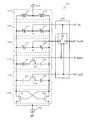
- FIG. 1 is a diagram showing an exemplary configuration of a voltage controlled oscillator 101 according to a first embodiment of the present invention.
- FIG. 2A is a diagram illustrating frequency characteristics of a conventional voltage controlled oscillator.
- FIG. 2B is a diagram illustrating frequency sensitivity characteristics of the conventional voltage controlled oscillator.
- FIG. 3A is a diagram illustrating frequency characteristics of the voltage controlled oscillator 101 according to the first embodiment.
- FIG. 3B is a diagram illustrating frequency sensitivity characteristics of the voltage controlled oscillator 101 according to the first embodiment.
- FIG. 4 is a diagram showing a detailed configuration of a frequency sensitivity controller 180 according to the first embodiment.
- FIG. 5 is a diagram showing an exemplary configuration of a voltage controlled oscillator 102 according to a second embodiment of the present invention.
- FIG. 6A is a diagram illustrating frequency characteristics of the voltage controlled oscillator 102 according to the second embodiment.
- FIG. 6B is a diagram illustrating frequency sensitivity characteristics of the voltage controlled oscillator 102 according to the second embodiment.
- FIG. 7 is a diagram showing a detailed configuration of a frequency sensitivity controller 180 according to the second embodiment.
- FIG. 8A is a diagram showing a configuration of a voltage controlled oscillator 103 according to a third embodiment of the present invention.
- FIG. 8B is a diagram showing a detailed connection within the frequency sensitivity controller 180 shown in FIG. 8A .
- FIG. 8C is a diagram showing another detailed connection within the frequency sensitivity controller 180 shown in FIG. 8A .
- FIG. 9A is a diagram illustrating frequency characteristics of the voltage controlled oscillator 103 according to the third embodiment.
- FIG. 9B is a diagram illustrating frequency sensitivity characteristics of the voltage controlled oscillator 103 according to the third embodiment.
- FIG. 10A is a diagram illustrating another variable capacitance circuit usable in the voltage controlled oscillator according to the present invention.
- FIG. 10B is a diagram illustrating another variable capacitance circuit usable in the voltage controlled oscillator according to the present invention.
- FIG. 10C is a diagram illustrating another variable capacitance circuit usable in the voltage controlled oscillator according to the present invention.
- FIG. 10D is a diagram illustrating another variable capacitance circuit usable in the voltage controlled oscillator according to the present invention.
- FIG. 10E is a diagram illustrating another capacitance switch circuit usable in the voltage controlled oscillator according to the present invention.
- FIG. 11 is a diagram showing a configuration of a PLL circuit 300 using the voltage controlled oscillator according to the present invention.
- FIG. 12 is a diagram showing a configuration of a wireless communication device using the PLL circuit shown in FIG. 11 .
- FIG. 13 is a diagram showing a configuration of a conventional voltage controlled oscillator 1 d.
- FIG. 14 is a diagram for illustrating a problem of the conventional voltage controlled oscillator 1 d.
- variable capacitance circuit 120 , 130 , 135 variable capacitance circuit
- variable capacitance element 121 , 122 , 131 , 132 , 136 , 137 variable capacitance element
- FIG. 1 is a diagram showing an exemplary configuration of a voltage controlled oscillator 101 according to a first embodiment of the present invention.
- the voltage controlled oscillator 101 of the first embodiment includes an inductor circuit 110 , a first variable capacitance circuit 120 , a second variable capacitance circuit 130 , a first capacitance switch circuit 140 , a second capacitance switch circuit 150 , a negative resistance circuit 160 , a current source 170 , and a frequency sensitivity controller 180 .
- the inductor circuit 110 , the first variable capacitance circuit 120 , the second variable capacitance circuit 130 , the first capacitance switch circuit 140 , the second capacitance switch circuit 150 , and the negative resistance circuit 160 are connected in parallel with each other, and thus form an oscillation circuit.
- the inductor circuit 110 includes inductors 111 and 112 connected in series, and a power supply voltage Vdd is supplied to a connection point between the inductors 111 and 112 .
- the negative resistance circuit 160 is formed with two transistors 161 and 162 being cross-coupled. MOS transistors or bipolar transistors are suitable as the transistors 161 and 162 .
- the first variable capacitance circuit 120 includes variable capacitance elements 121 and 122 connected in series, and a control voltage Vt for feedback control of an oscillation frequency is applied to a connection point A (e.g., a virtual ground point for differential signals) between the variable capacitance elements 121 and 122 .
- the second variable capacitance circuit 130 includes variable capacitance elements 131 and 132 connected in series, and the control voltage Vt or a control signal Fsell is applied, via the frequency sensitivity controller 180 , to a connection point B (e.g., a virtual ground point for differential signals) between the variable capacitance elements 131 and 132 .
- Each of the variable capacitance elements 121 , 122 , 131 , and 132 is a variable capacitance element that utilizes a gate capacitance used in a CMOS process.
- the first capacitance switch circuit 140 includes a MOS transistor 143 , and capacitors 141 and 142 which are connected to the drain and source of the MOS transistor 143 , respectively.
- a control signal Fsel 2 is applied to the gate of the MOS transistor 143 .
- the second capacitance switch circuit 150 includes a MOS transistor 153 , and capacitors 151 and 152 which are connected to the drain and source of the MOS transistor 153 , respectively.
- a control signal Fsel 3 is applied to the gate of the MOS transistor 153 .
- Each of the first and second capacitance switch circuits 140 and 150 forms a band-switch circuit.
- a frequency variable range of the voltage controlled oscillator 101 is determined based on four frequency ranges a (logical value 00), b (logical value 01), c (logical value 10), and d (logical value 11) ( FIG.
- an oscillation frequency (f) of the voltage controlled oscillator 101 is represented by the following equation, using: an inductance value L of the inductor circuit 110 ; a variable capacitance value Cv resulting from the variable capacitance circuits 120 and 130 ; and a fixed capacitance value Cc resulting from the capacitances of the capacitance switch circuits 140 and 150 and from a parasitic capacitance generated at the negative resistance circuit 160 and the like.
- the inductance value L is constant.
- the fixed capacitance value Cc differs among the four frequency ranges a to d.
- the fixed capacitance value Cc is minimum in the frequency range a which provides the highest oscillation frequency, and maximum in the frequency range d which provides the lowest oscillation frequency.
- the variable capacitance value Cv is the same value as long as the control voltage Vt is constant. Accordingly, in the foregoing equation, in the frequency range d providing the lowest oscillation frequency (f), a capacitance value ratio Cv/(Cc+Cv), which is a ratio of the variable capacitance value Cv to the total capacitance value Cc+Cv, is minimum, so that the frequency sensitivity decreases.
- the capacitance value ratio Cv/(Cc+Cv) is maximum, so that the frequency sensitivity increases.
- the frequency sensitivity controller 180 switches the control voltage Vt, which is applied to the connection point B of the second variable capacitance circuit 130 , to the control signal Fsel 1 . That is, the frequency sensitivity controller 180 causes the second variable capacitance circuit 130 to function as a fixed capacitance circuit, to thereby use the second variable capacitance circuit 130 as a band-switch circuit.
- the frequency sensitivity controller 180 applies the control signal Fsel 1 to the connection point B of the second variable capacitance circuit 130 , and switches between the high level and the low level.
- the high-frequency variable range a is divided into two, namely, a variable range ah (logical value 000), which is based on upper frequencies, and a variable range al (logical value 001), which is based on lower frequencies ( FIG. 3A ).
- the frequency sensitivity can be suppressed without narrowing the high-frequency variable range a ( FIG. 3B ).
- FIG. 4 A specific example of a circuit of the frequency sensitivity controller 180 for realizing the present embodiment is shown in FIG. 4 .
- the mark “*” denotes that the logical value may be either 1 or 0.
- FIG. 5 is a diagram showing an exemplary configuration of a voltage controlled oscillator 102 according to a second embodiment of the present invention. Here, a bias circuit and the like are omitted.
- the voltage controlled oscillator 102 of the second embodiment has a third variable capacitance circuit 135 , in addition to the same structure as that of the voltage controlled oscillator 101 of the first embodiment described above.
- the third variable capacitance circuit 135 includes variable capacitance elements 136 and 137 connected in series, and the control voltage Vt or the control signal Fsell is applied, via the frequency sensitivity controller 180 , to a connection point C (e.g., a virtual ground point for differential signals) between the variable capacitance elements 136 and 137 .
- the frequency sensitivity controller 180 applies the control voltage Vt or the control signal Fsell to the connection point C (e.g., a virtual ground point for differential signals) of the third variable capacitance circuit 135 , so that the third variable capacitance circuit 135 is used not only as the variable capacitance circuit but also as a band-switch circuit.
- the frequency sensitivity controller 180 applies the control signal Fsel 1 to the connection point B of the second variable capacitance circuit 130 , and switches between the high level and the low level. At this time, the control signal Fsel 1 is applied to the connection point C of the third variable capacitance circuit 135 .
- the frequency sensitivity controller 180 applies the control signal Fsel 1 to the connection point C of the third variable capacitance circuit 135 , and switches between the high level and the low level. At this time, the control voltage Vt is applied to the connection point B of the second variable capacitance circuit 130 .
- the frequency variable range a is divided into two, namely, a variable range ah (logical value 000), which is based on upper frequencies, and a variable range al (logical value 001), which is based on lower frequencies
- the frequency variable range b is divided into two, namely, a variable range bh (logical value 010), which is based on upper frequencies, and a variable range bl (logical value 011), which is based on lower frequencies ( FIG. 6A ).
- the frequency sensitivity can be suppressed without narrowing the high-frequency variable ranges a and b ( FIG. 6B ).
- FIG. 7 A specific example of a circuit of the frequency sensitivity controller 180 for realizing the present embodiment is shown in FIG. 7 .
- the mark “*” denotes that the logical value may be either 1 or 0.
- the configurations of the voltage controlled oscillators 101 and 102 shown in FIGS. 1 and 5 are merely examples.
- the voltage controlled oscillator according to the present invention may have any configuration, as long as the configuration includes two or more variable capacitance circuits and at least one capacitance switch circuit.
- use of a configuration shown in FIGS. 8A to 8C enables the following control.
- a high-band signal outputted from the voltage controlled oscillator is converted into a low-band signal via a 1/n frequency divider.
- a frequency sensitivity of the low-band signal outputted from the 1 /n frequency divider and a frequency sensitivity of the high-band signal outputted from the voltage controlled oscillator are made coincident with each other. For this purpose, therefore, it is necessary that, in a case of outputting the low-band signal, the frequency sensitivity of the signal outputted from the voltage controlled oscillator is n times higher than the frequency sensitivity in a case of outputting the high-band signal.
- FIGS. 8B and 8C As shown in these figures, seven variable capacitance circuits mosv 0 to mosv 6 , and one capacitance switch circuit sw are combined, so that a high band is divided into six frequency ranges and a low band is divided into three frequency ranges.
- the frequency sensitivity in the case of outputting the high-band can be set to approximately 1 ⁇ 2 of the frequency sensitivity in the case of outputting the low-band ( FIGS. 9A and 9B ).
- variable capacitance circuit of the voltage controlled oscillator not only the configuration shown in FIG. 1 and the like, but also a configuration using an Inversion type MOS transistor, an Accumulation type MOS transistor, or C-coupling may be adopted ( FIGS. 10A to 10D ).
- capacitance switch circuit of the voltage controlled oscillator according to the present invention not only the configuration shown in FIG. 1 and the like, but also a configuration shown in FIG. 10E may be adopted.
- FIG. 11 is a diagram showing an exemplary configuration of a PLL circuit 300 using any of the voltage controlled oscillators 101 to 103 according to the first to third embodiments of the present invention.
- the PLL circuit 300 includes a phase comparator 301 , a loop filter 302 , a voltage controlled oscillator 303 of the present invention, and a frequency divider 304 .
- the phase comparator 301 compares an inputted reference signal with a signal obtained by the frequency divider 304 dividing an output signal of the voltage controlled oscillator 303 .
- a signal outputted from the phase comparator 301 is inputted, as a control voltage Vt, to the voltage controlled oscillator 303 via the loop filter 302 .
- the voltage controlled oscillator 303 Based on the control voltage Vt, the voltage controlled oscillator 303 outputs a signal of a desired frequency.
- the PLL circuit 300 locks the desired frequency.
- a mixer may be used instead of the frequency divider 304 , or the frequency divider 304 and a mixer may be used in combination.
- FIG. 12 is a diagram showing an exemplary configuration of a wireless communication device 400 using the above-described PLL circuit 300 .
- the wireless communication device 400 includes an antenna 401 , a power amplifier 402 , a modulator 403 , a switch 404 , a low noise amplifier 405 , a demodulator 406 , and a PLL circuit 300 .
- the modulator 403 For transmitting a wireless signal, the modulator 403 modulates a desired radio frequency signal, which is outputted from the PLL circuit 300 , with a baseband modulation signal, and outputs the resulting signal.
- the modulated radio frequency signal outputted from the modulator 403 is amplified by the power amplifier 402 , and radiated from the antenna 401 via the switch 404 .
- a modulated radio frequency signal received by the antenna 401 is inputted to the low noise amplifier 405 via the switch 404 , amplified, and inputted to the demodulator 406 .
- the demodulator 406 demodulates the modulated radio frequency signal inputted thereto, into a baseband modulation signal by using the radio frequency signal outputted from the PLL circuit 300 .
- the PLL circuit 300 may be used at each of the transmitter side and the receiver side. Moreover, the PLL circuit 300 may serve also as a modulator.
- the voltage controlled oscillator according to the present invention makes it possible to, while suppressing deterioration of phase noise characteristics, variably control an oscillation frequency over a wide range with a frequency sensitivity being kept low.
- the voltage controlled oscillator according to the present invention is usable for, e.g., generating a local oscillation signal for a wireless communication device, and particularly useful in a case where, for example, an oscillation frequency is variably controlled over a wide range with a frequency sensitivity being kept low while deterioration of phase noise characteristics is suppressed.
Landscapes
- Engineering & Computer Science (AREA)
- Power Engineering (AREA)
- Inductance-Capacitance Distribution Constants And Capacitance-Resistance Oscillators (AREA)
- Stabilization Of Oscillater, Synchronisation, Frequency Synthesizers (AREA)
Abstract
Description
Claims (6)
Applications Claiming Priority (3)
| Application Number | Priority Date | Filing Date | Title |
|---|---|---|---|
| JP2008-086655 | 2008-03-28 | ||
| JP2008086655 | 2008-03-28 | ||
| PCT/JP2009/001189 WO2009119042A1 (en) | 2008-03-28 | 2009-03-17 | Voltage controlled oscillator, and pll circuit and wireless communication device using voltage controlled oscillator |
Publications (2)
| Publication Number | Publication Date |
|---|---|
| US20100171557A1 US20100171557A1 (en) | 2010-07-08 |
| US8067995B2 true US8067995B2 (en) | 2011-11-29 |
Family
ID=41113253
Family Applications (1)
| Application Number | Title | Priority Date | Filing Date |
|---|---|---|---|
| US12/601,621 Expired - Fee Related US8067995B2 (en) | 2008-03-28 | 2009-03-17 | Voltage controlled oscillator, and PLL circuit and wireless communication device each using the same |
Country Status (4)
| Country | Link |
|---|---|
| US (1) | US8067995B2 (en) |
| JP (1) | JPWO2009119042A1 (en) |
| CN (1) | CN101682293B (en) |
| WO (1) | WO2009119042A1 (en) |
Cited By (2)
| Publication number | Priority date | Publication date | Assignee | Title |
|---|---|---|---|---|
| US8253506B2 (en) * | 2010-10-05 | 2012-08-28 | Qualcomm, Incorporated | Wideband temperature compensated resonator and wideband VCO |
| US20170170822A1 (en) * | 2015-12-14 | 2017-06-15 | Skyworks Solutions, Inc. | Variable capacitor |
Families Citing this family (12)
| Publication number | Priority date | Publication date | Assignee | Title |
|---|---|---|---|---|
| EP2648193B1 (en) | 2012-04-03 | 2015-07-29 | Telefonaktiebolaget L M Ericsson (publ) | An inductor layout, and a voltage-controlled oscillator (VCO) system |
| DK2863429T3 (en) | 2013-10-16 | 2017-09-04 | ERICSSON TELEFON AB L M (publ) | Adjustable inductor device, transceiver, method and computer program |
| HUE052115T2 (en) | 2013-10-16 | 2021-04-28 | Ericsson Telefon Ab L M | Transceiver, receiver and communication device with switch arrangement |
| JP2015088930A (en) | 2013-10-30 | 2015-05-07 | セイコーエプソン株式会社 | Oscillation circuit, oscillator, method of manufacturing oscillator, electronic apparatus, and moving body |
| JP2015088931A (en) | 2013-10-30 | 2015-05-07 | セイコーエプソン株式会社 | Oscillation circuit, oscillator, method of manufacturing oscillator, electronic apparatus, and moving body |
| JP6226127B2 (en) | 2013-10-30 | 2017-11-08 | セイコーエプソン株式会社 | OSCILLATOR CIRCUIT, OSCILLATOR, METHOD FOR MANUFACTURING OSCILLATOR, ELECTRONIC DEVICE, AND MOBILE BODY |
| JP2015088876A (en) | 2013-10-30 | 2015-05-07 | セイコーエプソン株式会社 | Vibration element, vibrator, electronic device, electronic apparatus and movable body |
| JP6206664B2 (en) * | 2013-10-30 | 2017-10-04 | セイコーエプソン株式会社 | OSCILLATOR CIRCUIT, OSCILLATOR, METHOD FOR MANUFACTURING OSCILLATOR, ELECTRONIC DEVICE, AND MOBILE BODY |
| JP5789003B2 (en) * | 2014-01-07 | 2015-10-07 | ルネサスエレクトロニクス株式会社 | Oscillation circuit and semiconductor device |
| KR102581650B1 (en) * | 2018-06-28 | 2023-09-25 | 삼성전자주식회사 | Discrete capacitance switching circuit and capacitor array circuit including the same |
| CN111464179B (en) * | 2020-04-28 | 2024-03-01 | 恒玄科技(上海)股份有限公司 | Resonant frequency control circuit |
| CN114679197A (en) * | 2022-03-02 | 2022-06-28 | 维沃移动通信有限公司 | Radio frequency circuit, capacitance value control method thereof and electronic equipment |
Citations (6)
| Publication number | Priority date | Publication date | Assignee | Title |
|---|---|---|---|---|
| JP2003324316A (en) | 2002-05-08 | 2003-11-14 | Toshiba Corp | Voltage-controlled oscillator |
| US20030227341A1 (en) | 2002-06-06 | 2003-12-11 | Matsushita Electric Industrial Co., Ltd. | Voltage-controlled oscillator and frequency synthesizer |
| JP2004147310A (en) | 2002-10-03 | 2004-05-20 | Matsushita Electric Ind Co Ltd | Voltage controlled oscillator, wireless communication apparatus, and voltage controlled oscillation method |
| US20050190002A1 (en) | 2002-10-03 | 2005-09-01 | Koji Takinami | Voltage-controlled oscillator, radio communication apparatus and voltage-controlled oscillation method |
| US7170358B2 (en) * | 2004-06-15 | 2007-01-30 | Matsushita Electric Industrial Co., Ltd. | Voltage controlled oscillator, and PLL circuit and wireless communication apparatus using the same |
| US20070075798A1 (en) | 2005-09-30 | 2007-04-05 | Sharp Kabushiki Kaisha | Voltage control oscillator and voltage control oscillator unit |
Family Cites Families (2)
| Publication number | Priority date | Publication date | Assignee | Title |
|---|---|---|---|---|
| JP2005269310A (en) * | 2004-03-19 | 2005-09-29 | Nec Electronics Corp | Voltage controlled oscillator |
| US7102454B2 (en) * | 2004-08-04 | 2006-09-05 | Via Technologies, Inc. | Highly-linear signal-modulated voltage controlled oscillator |
-
2009
- 2009-03-17 WO PCT/JP2009/001189 patent/WO2009119042A1/en active Application Filing
- 2009-03-17 US US12/601,621 patent/US8067995B2/en not_active Expired - Fee Related
- 2009-03-17 JP JP2010505312A patent/JPWO2009119042A1/en active Pending
- 2009-03-17 CN CN2009800003897A patent/CN101682293B/en not_active Expired - Fee Related
Patent Citations (8)
| Publication number | Priority date | Publication date | Assignee | Title |
|---|---|---|---|---|
| JP2003324316A (en) | 2002-05-08 | 2003-11-14 | Toshiba Corp | Voltage-controlled oscillator |
| US20030227341A1 (en) | 2002-06-06 | 2003-12-11 | Matsushita Electric Industrial Co., Ltd. | Voltage-controlled oscillator and frequency synthesizer |
| JP2004015387A (en) | 2002-06-06 | 2004-01-15 | Matsushita Electric Ind Co Ltd | Voltage-controlled oscillator and frequency synthesizer |
| JP2004147310A (en) | 2002-10-03 | 2004-05-20 | Matsushita Electric Ind Co Ltd | Voltage controlled oscillator, wireless communication apparatus, and voltage controlled oscillation method |
| US20050190002A1 (en) | 2002-10-03 | 2005-09-01 | Koji Takinami | Voltage-controlled oscillator, radio communication apparatus and voltage-controlled oscillation method |
| US7170358B2 (en) * | 2004-06-15 | 2007-01-30 | Matsushita Electric Industrial Co., Ltd. | Voltage controlled oscillator, and PLL circuit and wireless communication apparatus using the same |
| US20070075798A1 (en) | 2005-09-30 | 2007-04-05 | Sharp Kabushiki Kaisha | Voltage control oscillator and voltage control oscillator unit |
| JP2007104152A (en) | 2005-09-30 | 2007-04-19 | Sharp Corp | Voltage controlled oscillator and voltage controlled oscillator unit |
Non-Patent Citations (1)
| Title |
|---|
| International Search Report issued Jun. 2, 2009 in International (PCT) Application No. PCT/JP2009/001189. |
Cited By (3)
| Publication number | Priority date | Publication date | Assignee | Title |
|---|---|---|---|---|
| US8253506B2 (en) * | 2010-10-05 | 2012-08-28 | Qualcomm, Incorporated | Wideband temperature compensated resonator and wideband VCO |
| US20170170822A1 (en) * | 2015-12-14 | 2017-06-15 | Skyworks Solutions, Inc. | Variable capacitor |
| US10129837B2 (en) * | 2015-12-14 | 2018-11-13 | Skyworks Solutions, Inc. | Variable capacitor |
Also Published As
| Publication number | Publication date |
|---|---|
| CN101682293A (en) | 2010-03-24 |
| JPWO2009119042A1 (en) | 2011-07-21 |
| US20100171557A1 (en) | 2010-07-08 |
| WO2009119042A1 (en) | 2009-10-01 |
| CN101682293B (en) | 2013-10-30 |
Similar Documents
| Publication | Publication Date | Title |
|---|---|---|
| US8067995B2 (en) | Voltage controlled oscillator, and PLL circuit and wireless communication device each using the same | |
| US8502614B2 (en) | Variable inductor, and oscillator and communication system using the same | |
| US6778022B1 (en) | VCO with high-Q switching capacitor bank | |
| US9236872B2 (en) | Voltage-controlled oscillator, signal generation apparatus, and electronic device | |
| US10516404B2 (en) | Voltage controlled oscillator using variable capacitor and phase locked loop using the same | |
| US6680657B2 (en) | Cross-coupled voltage controlled oscillator with improved phase noise performance | |
| CN100472976C (en) | Low and intermediate frequency wireless receiver with calibrating circuit | |
| JP4089938B2 (en) | Voltage controlled oscillator | |
| WO2006047041A1 (en) | Voltage controlled oscillator with varactor-less tuning | |
| US10205422B2 (en) | System and method for a voltage controlled oscillator | |
| US20090289732A1 (en) | Semiconductor integrated circuit device and frequency synthesizer | |
| US8031020B1 (en) | Bias circuit to reduce flicker noise in tunable LC oscillators | |
| US7626470B2 (en) | Voltage-controlled oscillator for multi-band and RF communication apparatus having the same | |
| US20150002236A1 (en) | Systems and Methods of Stacking LC Tanks for Wide Tuning Range and High Voltage Swing | |
| US7286024B2 (en) | Voltage-controlled oscillator with differential output | |
| US7567139B2 (en) | Voltage controlled oscillator, and PLL circuit and wireless communication apparatus using the same | |
| US20070146082A1 (en) | Frequency synthesizer, wireless communications device, and control method | |
| US7701304B2 (en) | Voltage controlled oscillator, and PLL circuit and radio communication apparatus using the same | |
| KR101855037B1 (en) | Sub-nyquist receiver of using pseudo random binary sequence generator | |
| US20210175850A1 (en) | Freqency synthesizer with phase noise temperature compensation, communication unit and method therefor | |
| US7724102B2 (en) | Oscillator circuit | |
| CN106374837B (en) | Quadrature voltage controlled oscillator | |
| US6842081B2 (en) | Dual frequency voltage controlled oscillator circuit | |
| US9106179B2 (en) | Voltage-controlled oscillators and related systems | |
| US7944318B2 (en) | Voltage controlled oscillator, and PLL circuit and radio communication device each including the same |
Legal Events
| Date | Code | Title | Description |
|---|---|---|---|
| AS | Assignment |
Owner name: PANASONIC CORPORATION, JAPAN Free format text: ASSIGNMENT OF ASSIGNORS INTEREST;ASSIGNOR:TSUKIZAWA, TAKAYUKI;REEL/FRAME:023849/0199 Effective date: 20091106 |
|
| ZAAA | Notice of allowance and fees due |
Free format text: ORIGINAL CODE: NOA |
|
| ZAAB | Notice of allowance mailed |
Free format text: ORIGINAL CODE: MN/=. |
|
| STCF | Information on status: patent grant |
Free format text: PATENTED CASE |
|
| FEPP | Fee payment procedure |
Free format text: PAYOR NUMBER ASSIGNED (ORIGINAL EVENT CODE: ASPN); ENTITY STATUS OF PATENT OWNER: LARGE ENTITY |
|
| FPAY | Fee payment |
Year of fee payment: 4 |
|
| MAFP | Maintenance fee payment |
Free format text: PAYMENT OF MAINTENANCE FEE, 8TH YEAR, LARGE ENTITY (ORIGINAL EVENT CODE: M1552); ENTITY STATUS OF PATENT OWNER: LARGE ENTITY Year of fee payment: 8 |
|
| FEPP | Fee payment procedure |
Free format text: MAINTENANCE FEE REMINDER MAILED (ORIGINAL EVENT CODE: REM.); ENTITY STATUS OF PATENT OWNER: LARGE ENTITY |
|
| LAPS | Lapse for failure to pay maintenance fees |
Free format text: PATENT EXPIRED FOR FAILURE TO PAY MAINTENANCE FEES (ORIGINAL EVENT CODE: EXP.); ENTITY STATUS OF PATENT OWNER: LARGE ENTITY |
|
| STCH | Information on status: patent discontinuation |
Free format text: PATENT EXPIRED DUE TO NONPAYMENT OF MAINTENANCE FEES UNDER 37 CFR 1.362 |
|
| FP | Lapsed due to failure to pay maintenance fee |
Effective date: 20231129 |