US8063509B2 - Power supply voltage adjusting apparatus, recording medium, and power supply voltage adjusting method - Google Patents
Power supply voltage adjusting apparatus, recording medium, and power supply voltage adjusting method Download PDFInfo
- Publication number
- US8063509B2 US8063509B2 US12/560,785 US56078509A US8063509B2 US 8063509 B2 US8063509 B2 US 8063509B2 US 56078509 A US56078509 A US 56078509A US 8063509 B2 US8063509 B2 US 8063509B2
- Authority
- US
- United States
- Prior art keywords
- power supply
- supply voltage
- voltage
- domain module
- clock signal
- Prior art date
- Legal status (The legal status is an assumption and is not a legal conclusion. Google has not performed a legal analysis and makes no representation as to the accuracy of the status listed.)
- Active, expires
Links
Images


Classifications
-
- H—ELECTRICITY
- H03—ELECTRONIC CIRCUITRY
- H03K—PULSE TECHNIQUE
- H03K19/00—Logic circuits, i.e. having at least two inputs acting on one output; Inverting circuits
- H03K19/0008—Arrangements for reducing power consumption
- H03K19/0016—Arrangements for reducing power consumption by using a control or a clock signal, e.g. in order to apply power supply
-
- G—PHYSICS
- G06—COMPUTING; CALCULATING OR COUNTING
- G06F—ELECTRIC DIGITAL DATA PROCESSING
- G06F1/00—Details not covered by groups G06F3/00 - G06F13/00 and G06F21/00
- G06F1/26—Power supply means, e.g. regulation thereof
- G06F1/32—Means for saving power
- G06F1/3203—Power management, i.e. event-based initiation of a power-saving mode
- G06F1/3234—Power saving characterised by the action undertaken
- G06F1/3296—Power saving characterised by the action undertaken by lowering the supply or operating voltage
-
- Y—GENERAL TAGGING OF NEW TECHNOLOGICAL DEVELOPMENTS; GENERAL TAGGING OF CROSS-SECTIONAL TECHNOLOGIES SPANNING OVER SEVERAL SECTIONS OF THE IPC; TECHNICAL SUBJECTS COVERED BY FORMER USPC CROSS-REFERENCE ART COLLECTIONS [XRACs] AND DIGESTS
- Y02—TECHNOLOGIES OR APPLICATIONS FOR MITIGATION OR ADAPTATION AGAINST CLIMATE CHANGE
- Y02D—CLIMATE CHANGE MITIGATION TECHNOLOGIES IN INFORMATION AND COMMUNICATION TECHNOLOGIES [ICT], I.E. INFORMATION AND COMMUNICATION TECHNOLOGIES AIMING AT THE REDUCTION OF THEIR OWN ENERGY USE
- Y02D10/00—Energy efficient computing, e.g. low power processors, power management or thermal management
Definitions
- FIG. 16 is an explanatory diagram of a principle of achieving lower power consumption with the ASV technique.
- a chart 1601 of FIG. 16 indicates the dependencies of the power consumption on manufacturing variation and the critical path delay for a fixed power supply voltage.
- a chart 1602 of FIG. 16 indicates the dependencies of the power consumption on manufacturing variation and the critical path delay for the ASV technique.
- a chip supplied with a fixed power supply voltage under the fast manufacturing variation condition is supplied with a voltage that is more than necessary regardless of low critical path delay.
- This excessive supply of the power supply voltage increases the leakage current, resulting in an increase in the power consumption. Therefore, as depicted in the chart 1602 , if the power supply voltage is adjusted to be reduced as much as possible within a range of the critical path satisfying the objective operation frequency according to the manufacturing variation, the power consumption may be reduced unless a chip has the slow manufacturing variation condition.
- Japanese Laid-Open Patent Publication No. 2005-100269 is not suitable for a multiple power source LSI having multiple power supply domains.
- a circuit may be configured across power supply domains of different voltages.
- a power supply voltage is obtained according to process variations in the multiple power source LSI, consideration may be given to combinations for each type of the power supply voltages. Therefore, as compared to the single power supply LSI, the number of processes for obtaining the power supply voltage increases considerably.
- the number of times I delay analysis is performed may be expressed by equation (1).
- I (number of times delay analysis performed) J ⁇ K L [times] (1)
- the clock skew (mismatch of clock timings) of the power supply domains of the multi power supply LSI may be corrected according to Japanese Laid-Open Patent Publication No. 2005-100269, the power supply voltage is not automatically adjustable according to process variations.
- the operation voltage sources are individually settable for the first group of circuits that generate clock signals and the second group of circuits that transfer signals and execute logical processing operations according to the clock signals, the power supply voltage is not automatically adjustable according to process variations.
- FIG. 19 is an explanatory diagram of delay times of a clock tree path and a logic path.
- a chart 1901 of FIG. 19 depicts an example in which the manufacturing variation dependency and the power supply voltage dependency are similar for the delay times of the clock tree circuit and the logic circuit.
- the logic path may be operated at the objective operation frequency by obtaining the AVS based on the characteristics of the clock tree path.
- the manufacturing variation dependency and the power supply voltage dependency may be different for delay times of the clock tree path and the logic path, and the difference may not be negligible in many cases.
- the manufacturing variation dependency of the logic path is greater, if the AVS is obtained based on the characteristics of the clock tree path, a problem arises in that the logic path is unable to operate at the objective operation frequency, causing malfunction.
- FIG. 1 is a block diagram of a multiple power source LSI according to the embodiment
- FIG. 2 is a timing chart comparing phases of a clock signal in the multiple power source LSI;
- FIG. 6 is a chart for a technique of setting the power supply voltage of a power supply domain B module
- FIG. 7 is a flowchart of a power supply voltage adjustment process for the power supply domain B module
- FIG. 8 is a block diagram of a configuration of a phase adjusting ASV control part
- FIG. 9 is a timing chart of an exemplary operation of the phase adjusting ASV control part
- FIG. 10 is a flowchart of a power supply voltage changing process in the power supply voltage adjustment of the power supply domain B module;
- FIG. 13 is a flowchart of a power supply voltage margin generating process
- FIG. 15 is a flowchart of a power supply voltage adjustment process that takes the power supply voltage margin into consideration
- a difference of the manufacturing variation dependency and the power supply voltage dependency is within a negligible range for delay times of a clock tree path and a logic path in each of modules.
- FIG. 1 is a block diagram of a configuration of a multiple power source LSI according to the embodiment.
- a multiple power source LSI 100 according to the embodiment includes a power supply domain A module 110 and a power supply domain B module 120 , respectively having different power supply voltages.
- the power supply domain A module 110 is connected to a power source IC 130 and the power supply domain B module 120 is connected to a power source IC 140 .
- the power supply domain A module 110 includes an ASV control part 111 , registers 112 and 113 , a clock tree 114 having a clock buffer within the power supply domain A module 110 , and logic circuit logics A and B.
- the power source IC 130 changes the voltage supplied to the power supply domain A module 110 according to a power supply voltage value output from the ASV control part 111 .
- the power supply domain B module 120 includes a phase adjusting ASV control part 121 , registers 122 and 123 , a clock tree 124 having a clock buffer within the power supply domain B module 120 , and a logic circuit logic C.
- the power source IC 140 changes the voltage supplied to the power supply domain B module 120 according to a power supply voltage value output from the phase adjusting ASV control part 121 .
- FIG. 2 is a timing chart comparing phases of the clock signal in the multiple power source LSI.
- FIG. 2 depicts the delay states of the clock signal at points of (1) tree 1 , (2) tree 2 , (3) tree 3 , and (4) tree 4 with respect to the clock signal of the power supply domain B module 120 of the multiple power source LSI 100 at point (0) depicted in FIG. 1 .
- the clock signal indicated by broken lines is detected and the phase is shifted as compared to the points of (1) tree 1 and (2) tree 2 in the power supply domain A module 110 . Therefore, when the power supply voltage of the power supply domain B module 120 is adjusted, the adjustment is performed to eliminate the shift of the phase and achieve the timing of the clock signal indicated by solid lines.
- configuration may be such that the clock signal input to the multiple power source LSI 100 is distributed to the power supply domains through a PLL circuit.
- the configuration may include a divider disposed at the downstream side of the PLL circuit to input clock signals of different clock cycles to the respective power supply domains.
- the ASV control part 111 functions as a voltage setting part and the phase adjusting ASV control part 121 functions as a detecting part and a voltage adjusting part to play the role of a power supply voltage adjusting apparatus.
- FIG. 3 is a chart for a technique of setting the power supply voltage of the power supply domain A module.
- a chart 300 of FIG. 3 depicts the power supply voltage dependency characteristics of the path delay in the power supply domain A module 110 .
- the chart 300 depicts the power supply voltage dependency characteristics of the respective process variations.
- FIG. 4 is a flowchart of a power supply voltage setting process for the power supply domain A module.
- the process variations and the power supply voltage dependency of the path delay time of the clock tree path are obtained (step S 401 ).
- step S 401 to obtain the process variations and the power supply voltage dependency, a circuit simulation may be performed with the use of the design data of the multiple power source LSI 100 or a characteristic test may actually be performed by the multiple power source LSI 100 .
- the delay value D 1 of the slow condition of the clock tree path is then obtained with the reference power supply voltage (A) of the power supply domain A module 110 (step S 402 ) and the power supply voltage (ASV-A) generating the delay value D 4 equivalent to the delay value D 1 is obtained according to each of the process variations (step S 403 ), ending a series of processes.
- the ASV value storage part 501 stores a value of the power supply voltage (ASV-A) obtained though the above power supply voltage setting process for the power supply domain A module 110 .
- the ASV value storage part 501 stores a power supply voltage (ASV-A′) according to a second embodiment described hereinafter.
- the ASV value storage part 501 may include, for example, a nonvolatile memory and may examine manufacturing variation of a chip, for example, at the time of the LSI test and write a power supply voltage value corresponding to the manufacturing variation at the time of the LSI test.
- the ASV value storage part 501 may include, for example, a volatile memory and may set a power supply voltage value corresponding to the manufacturing variation at a start-up routine of software when using the multiple power source LSI 100 .
- the power supply control part 502 reads and outputs the power supply voltage value (ASV-A, ASV-A′) stored in the ASV value storage part 501 , to the power source IC 130 according to the power supply voltage setting process for the power supply domain A module 110 .
- the ASV control part 111 executes the power supply voltage setting process for the power supply domain A module 110 as described above.
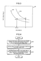
- FIG. 6 is a chart for a technique of setting the power supply voltage of the power supply domain B module.
- a chart 600 of FIG. 6 depicts the power supply voltage dependency characteristics of the path delay in the power supply domain B module 120 .
- the chart 600 depicts the power supply voltage dependency characteristics (characteristic curve fast, slow) of the respective process variations.
- the adjustment power supply voltage (ASV-A) is set through the power supply voltage setting process for the power supply domain A module 110 as described with reference to FIGS. 4 and 5 .
- the voltage of the reference power supply voltage (B) is adjusted to synchronize the clock signal of the power supply domain A module 110 and the clock signal of the power supply domain B module 120 .
- the voltage at which the clock signals synchronize is used as the adjustment power supply voltage (ASV-B).
- the path delay characteristic is maintained even when the power supply voltage of the power supply domain A module 110 is set from the reference power supply voltage (A) to the adjustment power supply voltage (ASV-A) by synchronizing the clock signals, when the power supply domain B module 120 power supply voltage is adjusted from the reference power supply voltage (B) to the adjustment power supply voltage (ASV-B), at a delay value D 3 the path delay characteristic at the delay value D 2 retained, as depicted in a chart 600 of FIG. 6 .
- FIG. 7 is a flowchart of a power supply voltage adjustment process for the power supply domain B module. As depicted in the flowchart of FIG. 7 , first, the power supply voltage of the power supply domain A module 110 is set by executing the processes at steps S 401 to S 403 described with reference to FIG. 4 .
- the power supply voltage of the power supply domain A is adjusted to ASV-A (step S 701 ).
- the power supply voltage supplied to the power supply domain B module 120 is adjusted so that the clock tree phase of the power supply domain B module 120 and the clock tree phase of the power supply domain A module 110 are in-phase (step S 702 ), and ending a series of processes.
- FIG. 8 is a block diagram of a configuration of the phase adjusting ASV control part.
- the phase adjusting ASV control part 121 includes a phase comparator 801 , a step value storage part 802 , a voltage code storage part 803 , an adder-subtracter 804 , and a power supply control circuit 805 .
- the phase comparator 801 compares the phases of the clock signal (clock A) flowing through the power supply domain A module 110 and the clock signal (clock B) flowing through the power supply domain B module 120 . As a result of this comparison, if the phase of the clock B has advanced more, an output signal DOWN is turned to “High” and conversely, if the phase of the clock A has advanced more, an output signal UP is turned to “High” and the respective signals are output to the adder-subtracter 804 .
- the step value storage part 802 stores a change step value at the time of the adjustment of the power supply voltage.
- the change step value is a part of adjustment when the power supply voltage is increased or reduced. For example, a step value of 0.01 [V] is stored.
- the voltage code storage part 803 stores a power supply voltage code corresponding to the current value of the power supply voltage.
- the adder-subtracter 804 adds or subtracts the change step value stored in the step value storage part 802 to/from the power supply voltage code stored in the voltage code storage part 803 .
- the power supply control circuit 805 controls the adder-subtracter 804 and outputs to the power source IC 140 , an instruction for changing the power supply voltage.
- the power supply control circuit 805 outputs a WE signal for adjusting the power supply voltage code stored in the voltage code storage part 803 according to changes in the power supply voltage supplied to the power supply domain B module 120 .
- FIG. 9 is a timing chart of an exemplary operation of the phase adjusting ASV control part. As depicted in FIG. 9 , if the clock B has advanced more than the clock A, the output signal DOWN of the phase comparator 801 is turned to “High” to perform an operation of reducing the power supply voltage by one step.
- the adder-subtracter 804 works as an adder when the output signal UP of the phase comparator 801 is “High” and as a subtracter when the output signal DOWN is “High”.
- the adder-subtracter 804 Since the step value storage part 802 stores the change step value of 0.01 [V] as described above, the adder-subtracter 804 outputs the power supply voltage code of 0.79 [V] obtained by subtracting 0.01 [V], i.e., one step from 0.80 [V].
- the WE signal causes the value stored in the voltage code storage part 803 to be changed to and stored as a power supply voltage code corresponding to 0.79 [V].
- the power source IC 140 instructed, by the power supply control circuit 805 , to change the power supply voltage changes the power supply voltage to 0.79 [V].
- the phase adjusting ASV control part 121 is configured to compare the phases of the clock signals (clock A, clock B) at the ends of the clock trees of the power supply domains, determine which has advanced more, and reduce or increase the power supply voltage depending on the result thereof.
- the two clock signals (clock A, clock B) are synchronized and therefore, the power supply voltage of the power supply domain B module 120 is the adjusted voltage, i.e., the adjustment power supply voltage (ASV-B), and a series of processes ends.
- the processes at steps S 1001 to S 1004 correspond to the process at step S 702 of the flowchart of FIG. 7 .
- the output signal turning to “High” corresponds to a case when too much time is required to change the power supply voltage from the upper limit to the lower limit and so the time required to change the power supply voltage is reduced to 1 ⁇ 2 by setting the initial value of the current value of the power supply voltage code to an intermediate value.
- the multiple power source LSI 100 of the first embodiment adjusts the power supply voltage with the use of the phase difference of the clock signals between the different power supply domain modules. Therefore, the processes concerning the power supply voltage are considerably reduced as compared to conventional technologies.
- the process taking 10 days in the case of 10 computers arranged to operate in parallel may be reduced by the number K of the power supply voltage conditions. If the power supply voltage dependency characteristics of the respective process variation conditions as depicted in FIG. 3 have been obtained through circuit simulations, the process may also be reduced by the number J of the process variation conditions.
- the multiple power source LSI 100 of the first embodiment may adjust the power supply voltages of the power supply domains to suitable power supply voltages according to the manufacturing variations with a fewer number of processes.
- the power supply voltage adjustment is performed with consideration of the manufacturing variation dependency and the power supply voltage dependency.
- the ASV may be obtained taking the difference into consideration.
- the configuration of the multiple power source LSI 100 of the second embodiment is identical to the configuration of the first embodiment and will not be described.
- the ASV control part 111 and the phase adjusting ASV control part 121 also function as the power supply voltage adjusting apparatus according to the embodiment.
- FIGS. 11 and 12 are charts for the power supply voltage adjustment technique that takes into consideration manufacturing variation dependency and power supply voltage dependency.
- the reference power supply voltage (A) is a reference point as depicted in FIG. 11 and the reference power supply voltage (B) is a reference point as depicted in FIG. 12 .
- this fluctuation range may be generated as a power supply voltage margin to set the power supply voltage giving consideration to the manufacturing variation corresponding to the power supply voltage margin.
- the power supply voltage within an operative frequency range may be supplied to prevent malfunction by supplying the module with a margin adjustment power supply voltage that is the power supply voltage reduced by the power supply voltage margin.
- the following two-stage process is performed for adjustment of the power supply voltages of two power supply domain modules with consideration of the power supply voltage margin as described above,
- FIG. 13 is a flowchart of a power supply voltage margin generating process.
- the process variations and the power supply voltage dependency of the path delay time of the clock tree path are obtained (step S 1301 ).
- the power supply voltage dependency characteristics may be obtained for the respective process variations indicated by solid lines in the charts 1100 and 1200 (see FIGS. 11 and 12 ).
- the range of the delay value under the fast condition is then obtained using the reference power supply voltage (B) as a reference point according to the manufacturing variation of the power supply domain B module 120 (step S 1302 ).
- the range of the delay value obtained at step S 1302 represents the fluctuation range of the delay value under the fast condition with consideration of the manufacturing variation of the power supply domain B module 120 .
- This range of the delay value corresponds to a range L 2 represented by dot-and-dash curves in a chart 1200 of FIG. 12 .
Landscapes
- Engineering & Computer Science (AREA)
- Theoretical Computer Science (AREA)
- Physics & Mathematics (AREA)
- General Engineering & Computer Science (AREA)
- General Physics & Mathematics (AREA)
- Computer Hardware Design (AREA)
- Computing Systems (AREA)
- Mathematical Physics (AREA)
- Semiconductor Integrated Circuits (AREA)
- Direct Current Feeding And Distribution (AREA)
- Power Sources (AREA)
Abstract
Description
I (number of times delay analysis performed)=J×K L [times] (1)
I=J×K L=5×54=3125 [times] (2)
Claims (6)
Applications Claiming Priority (1)
| Application Number | Priority Date | Filing Date | Title |
|---|---|---|---|
| PCT/JP2007/055671 WO2008114416A1 (en) | 2007-03-20 | 2007-03-20 | Power supply voltage regulator, recording medium and power supply voltage regulating method |
Related Parent Applications (1)
| Application Number | Title | Priority Date | Filing Date |
|---|---|---|---|
| PCT/JP2007/055671 Continuation WO2008114416A1 (en) | 2007-03-20 | 2007-03-20 | Power supply voltage regulator, recording medium and power supply voltage regulating method |
Publications (2)
| Publication Number | Publication Date |
|---|---|
| US20100164286A1 US20100164286A1 (en) | 2010-07-01 |
| US8063509B2 true US8063509B2 (en) | 2011-11-22 |
Family
ID=39765537
Family Applications (1)
| Application Number | Title | Priority Date | Filing Date |
|---|---|---|---|
| US12/560,785 Active 2027-05-23 US8063509B2 (en) | 2007-03-20 | 2009-09-16 | Power supply voltage adjusting apparatus, recording medium, and power supply voltage adjusting method |
Country Status (3)
| Country | Link |
|---|---|
| US (1) | US8063509B2 (en) |
| JP (1) | JPWO2008114416A1 (en) |
| WO (1) | WO2008114416A1 (en) |
Cited By (2)
| Publication number | Priority date | Publication date | Assignee | Title |
|---|---|---|---|---|
| US20110210780A1 (en) * | 2010-02-26 | 2011-09-01 | Hynix Semiconductor Inc. | Semiconductor integrated circuit |
| US10082861B2 (en) | 2015-08-31 | 2018-09-25 | Socionext Inc. | Power supply voltage control circuit device and power supply voltage control method |
Families Citing this family (10)
| Publication number | Priority date | Publication date | Assignee | Title |
|---|---|---|---|---|
| JP5487627B2 (en) * | 2009-01-27 | 2014-05-07 | 富士通セミコンダクター株式会社 | Semiconductor integrated circuit |
| JP5481871B2 (en) * | 2009-02-17 | 2014-04-23 | 富士通セミコンダクター株式会社 | Multi-power supply system, semiconductor integrated circuit |
| JPWO2011114416A1 (en) * | 2010-03-15 | 2013-06-27 | ケイレックス・テクノロジー株式会社 | Semiconductor integrated circuit power supply voltage determination method and semiconductor integrated circuit power supply voltage control system |
| US9939827B1 (en) * | 2011-12-16 | 2018-04-10 | Altera Corporation | Temperature dependent power supply circuitry |
| US9419589B2 (en) * | 2013-08-16 | 2016-08-16 | Apple Inc. | Power source for clock distribution network |
| CN103926996B (en) * | 2014-05-08 | 2016-06-08 | 上海航天电子通讯设备研究所 | A kind of FPGA zero dy namics power consumption method of design |
| CN105068587A (en) * | 2015-07-20 | 2015-11-18 | 广东电网有限责任公司云浮供电局 | Voltage regulating method of vectors of broad-width sine waves of transformer |
| US10114920B1 (en) * | 2016-06-29 | 2018-10-30 | Cadence Design Systems, Inc. | Method and apparatus for performing sign-off timing analysis of circuit designs using inter-power domain logic |
| CN114003079B (en) * | 2020-07-28 | 2023-08-08 | 瑞昱半导体股份有限公司 | Circuit applied to multiple power domains |
| CN115220508A (en) * | 2021-04-15 | 2022-10-21 | 中兴通讯股份有限公司 | Voltage adjusting method and device, computer equipment and readable medium |
Citations (20)
| Publication number | Priority date | Publication date | Assignee | Title |
|---|---|---|---|---|
| JPH08136621A (en) | 1994-11-11 | 1996-05-31 | Oki Electric Ind Co Ltd | Power-supply voltage supplying device |
| WO1997024806A1 (en) | 1995-12-28 | 1997-07-10 | Advantest Corporation | Semiconductor integrated circuit device with delay error correcting circuit |
| WO1998006022A2 (en) | 1996-08-07 | 1998-02-12 | Motorola Semiconducteurs S.A. | Methods and circuits for dynamically adjusting a supply voltage and/or a frequency of a clock signal in a digital circuit |
| JPH1139868A (en) | 1997-07-18 | 1999-02-12 | Matsushita Electric Ind Co Ltd | Semiconductor integrated circuit system, semiconductor integrated circuit and method of driving semiconductor integrated circuit system |
| JPH11296243A (en) | 1998-04-13 | 1999-10-29 | Fujitsu Ltd | Power supply voltage adjusting circuit, semiconductor device and method for adjusting power supply voltage of semiconductor device |
| JP2000035831A (en) * | 1998-07-21 | 2000-02-02 | Nec Corp | Low skew clock tree circuit using variable threshold voltage transistor |
| JP2002312058A (en) | 2001-04-11 | 2002-10-25 | Mitsubishi Electric Corp | Semiconductor integrated circuit |
| US20040145397A1 (en) * | 2000-01-24 | 2004-07-29 | Lutkemeyer Christian A.J. | System and method for compensating for supply voltage induced clock delay mismatches |
| JP2004253595A (en) * | 2003-02-20 | 2004-09-09 | Nec Corp | Semiconductor integrated circuit and skew controlling method |
| JP2004362398A (en) | 2003-06-06 | 2004-12-24 | Matsushita Electric Ind Co Ltd | Semiconductor integrated circuit |
| WO2005008777A1 (en) | 2003-07-22 | 2005-01-27 | Nec Corporation | Multi-power source semiconductor device |
| US6864600B2 (en) * | 2001-02-09 | 2005-03-08 | National Semiconductor Corporation | Apparatus and method for providing multiple power supply voltages to an integrated circuit |
| JP2005100269A (en) | 2003-09-26 | 2005-04-14 | Toshiba Microelectronics Corp | Semiconductor integrated circuit |
| JP2005115944A (en) | 2003-10-06 | 2005-04-28 | Hewlett-Packard Development Co Lp | Synchronization system and synchronization method of multiple variable-frequency clock generators |
| US20050253462A1 (en) * | 2004-02-06 | 2005-11-17 | Agere Systems Inc. | Integrated circuit with multiple power domains |
| US20060061401A1 (en) | 2004-09-17 | 2006-03-23 | Shinichiro Shiratake | Semiconductor device adapted to minimize clock skew |
| JP2006093249A (en) | 2004-09-22 | 2006-04-06 | Matsushita Electric Ind Co Ltd | Semiconductor integrated circuit |
| JP2006287163A (en) * | 2005-04-05 | 2006-10-19 | Renesas Technology Corp | Semiconductor integrated circuit |
| JP2006293856A (en) * | 2005-04-13 | 2006-10-26 | Toshiba Corp | Clock wiring device, and clock wiring method |
| JP2006339521A (en) * | 2005-06-03 | 2006-12-14 | Matsushita Electric Ind Co Ltd | Semiconductor integrated circuit |
-
2007
- 2007-03-20 WO PCT/JP2007/055671 patent/WO2008114416A1/en active Application Filing
- 2007-03-20 JP JP2009505015A patent/JPWO2008114416A1/en active Pending
-
2009
- 2009-09-16 US US12/560,785 patent/US8063509B2/en active Active
Patent Citations (24)
| Publication number | Priority date | Publication date | Assignee | Title |
|---|---|---|---|---|
| JPH08136621A (en) | 1994-11-11 | 1996-05-31 | Oki Electric Ind Co Ltd | Power-supply voltage supplying device |
| WO1997024806A1 (en) | 1995-12-28 | 1997-07-10 | Advantest Corporation | Semiconductor integrated circuit device with delay error correcting circuit |
| WO1998006022A2 (en) | 1996-08-07 | 1998-02-12 | Motorola Semiconducteurs S.A. | Methods and circuits for dynamically adjusting a supply voltage and/or a frequency of a clock signal in a digital circuit |
| JP2001505676A (en) | 1996-08-07 | 2001-04-24 | モトローラ・セミコンデュクトゥール・ソシエテ・アノニム | Method and circuit for dynamically adjusting the supply voltage and / or the frequency of a clock signal in a digital circuit |
| JPH1139868A (en) | 1997-07-18 | 1999-02-12 | Matsushita Electric Ind Co Ltd | Semiconductor integrated circuit system, semiconductor integrated circuit and method of driving semiconductor integrated circuit system |
| JPH11296243A (en) | 1998-04-13 | 1999-10-29 | Fujitsu Ltd | Power supply voltage adjusting circuit, semiconductor device and method for adjusting power supply voltage of semiconductor device |
| JP2000035831A (en) * | 1998-07-21 | 2000-02-02 | Nec Corp | Low skew clock tree circuit using variable threshold voltage transistor |
| US20040145397A1 (en) * | 2000-01-24 | 2004-07-29 | Lutkemeyer Christian A.J. | System and method for compensating for supply voltage induced clock delay mismatches |
| US6864600B2 (en) * | 2001-02-09 | 2005-03-08 | National Semiconductor Corporation | Apparatus and method for providing multiple power supply voltages to an integrated circuit |
| JP2002312058A (en) | 2001-04-11 | 2002-10-25 | Mitsubishi Electric Corp | Semiconductor integrated circuit |
| JP2004253595A (en) * | 2003-02-20 | 2004-09-09 | Nec Corp | Semiconductor integrated circuit and skew controlling method |
| JP2004362398A (en) | 2003-06-06 | 2004-12-24 | Matsushita Electric Ind Co Ltd | Semiconductor integrated circuit |
| US20060232316A1 (en) | 2003-07-22 | 2006-10-19 | Nec Corporation | Multi-power source semiconductor device |
| WO2005008777A1 (en) | 2003-07-22 | 2005-01-27 | Nec Corporation | Multi-power source semiconductor device |
| JP2005100269A (en) | 2003-09-26 | 2005-04-14 | Toshiba Microelectronics Corp | Semiconductor integrated circuit |
| JP2005115944A (en) | 2003-10-06 | 2005-04-28 | Hewlett-Packard Development Co Lp | Synchronization system and synchronization method of multiple variable-frequency clock generators |
| US20050253462A1 (en) * | 2004-02-06 | 2005-11-17 | Agere Systems Inc. | Integrated circuit with multiple power domains |
| JP2006086455A (en) | 2004-09-17 | 2006-03-30 | Toshiba Corp | Semiconductor device |
| US20060061401A1 (en) | 2004-09-17 | 2006-03-23 | Shinichiro Shiratake | Semiconductor device adapted to minimize clock skew |
| US7236035B2 (en) | 2004-09-17 | 2007-06-26 | Kabushiki Kaisha Toshiba | Semiconductor device adapted to minimize clock skew |
| JP2006093249A (en) | 2004-09-22 | 2006-04-06 | Matsushita Electric Ind Co Ltd | Semiconductor integrated circuit |
| JP2006287163A (en) * | 2005-04-05 | 2006-10-19 | Renesas Technology Corp | Semiconductor integrated circuit |
| JP2006293856A (en) * | 2005-04-13 | 2006-10-26 | Toshiba Corp | Clock wiring device, and clock wiring method |
| JP2006339521A (en) * | 2005-06-03 | 2006-12-14 | Matsushita Electric Ind Co Ltd | Semiconductor integrated circuit |
Non-Patent Citations (7)
| Title |
|---|
| Form PCT/ISA/237, mailed Jun. 19, 2007, in corresponding International Application No. PCT/JP2007/055671. |
| International Preliminary Report on Patentability, mailed Sep. 22, 2009, in corresponding International Application No. PCT/JP2007/055671 (8 pp.). |
| International Search Report, mailed Jun. 19, 2007, in corresponding International Application No. PCT/JP2007/055671. |
| Japanese Patent Office Notice of Rejection mailed Feb. 15, 2011 for corresponding Japanese Patent Application No. 2009-505015. |
| Japanese Patent Office Notice of Rejection mailed May 17, 2011, for corresponding Japanese Patent Application 2009-505015. |
| Machine Translations for each of the Japanese Patent Documents. * |
| Tschanz, J. et al., Effectiveness of Adaptive Supply Voltage and Body Bias for Reducing Impact of Parameter Variations in Low Power and High Performance Microprocessors, IEEE Journal of Solid-State Circuits, vol. 38, No. 5, May 2003, pp. 826-829. |
Cited By (3)
| Publication number | Priority date | Publication date | Assignee | Title |
|---|---|---|---|---|
| US20110210780A1 (en) * | 2010-02-26 | 2011-09-01 | Hynix Semiconductor Inc. | Semiconductor integrated circuit |
| US8489902B2 (en) * | 2010-02-26 | 2013-07-16 | SK Hynix Inc. | Semiconductor integrated circuit |
| US10082861B2 (en) | 2015-08-31 | 2018-09-25 | Socionext Inc. | Power supply voltage control circuit device and power supply voltage control method |
Also Published As
| Publication number | Publication date |
|---|---|
| US20100164286A1 (en) | 2010-07-01 |
| WO2008114416A1 (en) | 2008-09-25 |
| JPWO2008114416A1 (en) | 2010-07-01 |
Similar Documents
| Publication | Publication Date | Title |
|---|---|---|
| US8063509B2 (en) | Power supply voltage adjusting apparatus, recording medium, and power supply voltage adjusting method | |
| JP4894014B2 (en) | Adaptive control of power supplies for integrated circuits. | |
| US9244515B2 (en) | Semiconductor device comprising delay monitor and discrete supply switches | |
| US20090115468A1 (en) | Integrated Circuit and Method for Operating an Integrated Circuit | |
| US7930577B2 (en) | Closed-loop control for performance tuning | |
| US8381009B2 (en) | Device and method for power management | |
| US7554365B2 (en) | Glitch-free clock switching circuit | |
| JP2009200739A (en) | Semiconductor integrated circuit | |
| US9310878B2 (en) | Power gated and voltage biased memory circuit for reducing power | |
| US20090315601A1 (en) | Device and method for timing error management | |
| US20220345117A1 (en) | Hybrid Pulse/Two-Stage Data Latch | |
| US20200411067A1 (en) | Voltage regulation system for memory bit cells | |
| US8937511B2 (en) | Frequency scaling of variable speed systems for fast response and power reduction | |
| US20080056017A1 (en) | Data output apparatus, memory system, data output method, and data processing method | |
| KR20220110856A (en) | Serial data receiver with decision feedback equalization | |
| JP5131370B2 (en) | Power supply voltage adjusting device and power supply voltage adjusting method | |
| US7188325B1 (en) | Method for selecting transistor threshold voltages in an integrated circuit | |
| US11196435B1 (en) | Anti-aliasing techniques for time-to-digital converters | |
| JP5481871B2 (en) | Multi-power supply system, semiconductor integrated circuit | |
| US9455708B2 (en) | Dynamically adjustable circuit with circuit of characterized-path and method for generating circuit of characterized-path | |
| CN114706449B (en) | Frequency control method, circuit and chip based on self-adaptive clock | |
| JP2012100058A (en) | Delay circuit, delay control device, memory control device and information terminal apparatus | |
| CN113193866A (en) | Complementary Metal Oxide Semiconductor (CMOS) inverter circuit device | |
| US11474584B2 (en) | Semiconductor device having clock control circuit of adjusting speed of increasing clock frequency | |
| US8710890B2 (en) | Variable delay line for delay locked loop |
Legal Events
| Date | Code | Title | Description |
|---|---|---|---|
| AS | Assignment |
Owner name: FUJITSU LIMITED,JAPAN Free format text: ASSIGNMENT OF ASSIGNORS INTEREST;ASSIGNOR:OKANO, HIROSHI;REEL/FRAME:023262/0409 Effective date: 20090717 Owner name: FUJITSU LIMITED, JAPAN Free format text: ASSIGNMENT OF ASSIGNORS INTEREST;ASSIGNOR:OKANO, HIROSHI;REEL/FRAME:023262/0409 Effective date: 20090717 |
|
| FEPP | Fee payment procedure |
Free format text: PAYOR NUMBER ASSIGNED (ORIGINAL EVENT CODE: ASPN); ENTITY STATUS OF PATENT OWNER: LARGE ENTITY |
|
| STCF | Information on status: patent grant |
Free format text: PATENTED CASE |
|
| FPAY | Fee payment |
Year of fee payment: 4 |
|
| MAFP | Maintenance fee payment |
Free format text: PAYMENT OF MAINTENANCE FEE, 8TH YEAR, LARGE ENTITY (ORIGINAL EVENT CODE: M1552); ENTITY STATUS OF PATENT OWNER: LARGE ENTITY Year of fee payment: 8 |
|
| MAFP | Maintenance fee payment |
Free format text: PAYMENT OF MAINTENANCE FEE, 12TH YEAR, LARGE ENTITY (ORIGINAL EVENT CODE: M1553); ENTITY STATUS OF PATENT OWNER: LARGE ENTITY Year of fee payment: 12 |