US8042950B2 - Projection apparatus and image display apparatus with individual color light diffusion and microlens array - Google Patents
Projection apparatus and image display apparatus with individual color light diffusion and microlens array Download PDFInfo
- Publication number
- US8042950B2 US8042950B2 US12/309,924 US30992407A US8042950B2 US 8042950 B2 US8042950 B2 US 8042950B2 US 30992407 A US30992407 A US 30992407A US 8042950 B2 US8042950 B2 US 8042950B2
- Authority
- US
- United States
- Prior art keywords
- section
- lights
- individual
- color
- color lights
- Prior art date
- Legal status (The legal status is an assumption and is not a legal conclusion. Google has not performed a legal analysis and makes no representation as to the accuracy of the status listed.)
- Expired - Fee Related, expires
Links
- 238000009792 diffusion process Methods 0.000 title claims abstract description 23
- 230000003287 optical effect Effects 0.000 claims abstract description 181
- 239000004973 liquid crystal related substance Substances 0.000 claims abstract description 106
- 239000011159 matrix material Substances 0.000 claims abstract description 15
- 239000000758 substrate Substances 0.000 claims description 25
- 239000003086 colorant Substances 0.000 claims description 21
- 239000004065 semiconductor Substances 0.000 claims description 6
- 238000009826 distribution Methods 0.000 claims description 5
- 230000004044 response Effects 0.000 claims description 3
- 238000010586 diagram Methods 0.000 description 22
- 230000009471 action Effects 0.000 description 11
- 239000013307 optical fiber Substances 0.000 description 8
- 238000000926 separation method Methods 0.000 description 6
- 239000004983 Polymer Dispersed Liquid Crystal Substances 0.000 description 4
- 230000008859 change Effects 0.000 description 4
- 230000000694 effects Effects 0.000 description 4
- 230000000737 periodic effect Effects 0.000 description 4
- 229910003327 LiNbO3 Inorganic materials 0.000 description 3
- 239000013078 crystal Substances 0.000 description 3
- 239000010408 film Substances 0.000 description 3
- 230000007257 malfunction Effects 0.000 description 3
- 230000004048 modification Effects 0.000 description 3
- 238000012986 modification Methods 0.000 description 3
- 239000010453 quartz Substances 0.000 description 3
- VYPSYNLAJGMNEJ-UHFFFAOYSA-N silicon dioxide Inorganic materials O=[Si]=O VYPSYNLAJGMNEJ-UHFFFAOYSA-N 0.000 description 3
- 229910009372 YVO4 Inorganic materials 0.000 description 2
- 230000005540 biological transmission Effects 0.000 description 2
- 230000001678 irradiating effect Effects 0.000 description 2
- 230000010287 polarization Effects 0.000 description 2
- 229920000642 polymer Polymers 0.000 description 2
- 125000006850 spacer group Chemical group 0.000 description 2
- 239000010409 thin film Substances 0.000 description 2
- 229910001218 Gallium arsenide Inorganic materials 0.000 description 1
- 239000004020 conductor Substances 0.000 description 1
- 230000003247 decreasing effect Effects 0.000 description 1
- 230000005684 electric field Effects 0.000 description 1
- AMGQUBHHOARCQH-UHFFFAOYSA-N indium;oxotin Chemical compound [In].[Sn]=O AMGQUBHHOARCQH-UHFFFAOYSA-N 0.000 description 1
- 238000000034 method Methods 0.000 description 1
- 230000010355 oscillation Effects 0.000 description 1
- 230000009467 reduction Effects 0.000 description 1
- 239000011347 resin Substances 0.000 description 1
- 229920005989 resin Polymers 0.000 description 1
- 238000005549 size reduction Methods 0.000 description 1
Images


Classifications
-
- G—PHYSICS
- G02—OPTICS
- G02B—OPTICAL ELEMENTS, SYSTEMS OR APPARATUS
- G02B19/00—Condensers, e.g. light collectors or similar non-imaging optics
- G02B19/0004—Condensers, e.g. light collectors or similar non-imaging optics characterised by the optical means employed
- G02B19/0009—Condensers, e.g. light collectors or similar non-imaging optics characterised by the optical means employed having refractive surfaces only
- G02B19/0014—Condensers, e.g. light collectors or similar non-imaging optics characterised by the optical means employed having refractive surfaces only at least one surface having optical power
-
- G—PHYSICS
- G03—PHOTOGRAPHY; CINEMATOGRAPHY; ANALOGOUS TECHNIQUES USING WAVES OTHER THAN OPTICAL WAVES; ELECTROGRAPHY; HOLOGRAPHY
- G03B—APPARATUS OR ARRANGEMENTS FOR TAKING PHOTOGRAPHS OR FOR PROJECTING OR VIEWING THEM; APPARATUS OR ARRANGEMENTS EMPLOYING ANALOGOUS TECHNIQUES USING WAVES OTHER THAN OPTICAL WAVES; ACCESSORIES THEREFOR
- G03B21/00—Projectors or projection-type viewers; Accessories therefor
-
- G—PHYSICS
- G02—OPTICS
- G02B—OPTICAL ELEMENTS, SYSTEMS OR APPARATUS
- G02B19/00—Condensers, e.g. light collectors or similar non-imaging optics
- G02B19/0033—Condensers, e.g. light collectors or similar non-imaging optics characterised by the use
- G02B19/0047—Condensers, e.g. light collectors or similar non-imaging optics characterised by the use for use with a light source
- G02B19/0052—Condensers, e.g. light collectors or similar non-imaging optics characterised by the use for use with a light source the light source comprising a laser diode
- G02B19/0057—Condensers, e.g. light collectors or similar non-imaging optics characterised by the use for use with a light source the light source comprising a laser diode in the form of a laser diode array, e.g. laser diode bar
-
- G—PHYSICS
- G02—OPTICS
- G02B—OPTICAL ELEMENTS, SYSTEMS OR APPARATUS
- G02B27/00—Optical systems or apparatus not provided for by any of the groups G02B1/00 - G02B26/00, G02B30/00
- G02B27/09—Beam shaping, e.g. changing the cross-sectional area, not otherwise provided for
- G02B27/0927—Systems for changing the beam intensity distribution, e.g. Gaussian to top-hat
-
- G—PHYSICS
- G02—OPTICS
- G02B—OPTICAL ELEMENTS, SYSTEMS OR APPARATUS
- G02B27/00—Optical systems or apparatus not provided for by any of the groups G02B1/00 - G02B26/00, G02B30/00
- G02B27/09—Beam shaping, e.g. changing the cross-sectional area, not otherwise provided for
- G02B27/0938—Using specific optical elements
- G02B27/0944—Diffractive optical elements, e.g. gratings, holograms
-
- G—PHYSICS
- G02—OPTICS
- G02F—OPTICAL DEVICES OR ARRANGEMENTS FOR THE CONTROL OF LIGHT BY MODIFICATION OF THE OPTICAL PROPERTIES OF THE MEDIA OF THE ELEMENTS INVOLVED THEREIN; NON-LINEAR OPTICS; FREQUENCY-CHANGING OF LIGHT; OPTICAL LOGIC ELEMENTS; OPTICAL ANALOGUE/DIGITAL CONVERTERS
- G02F1/00—Devices or arrangements for the control of the intensity, colour, phase, polarisation or direction of light arriving from an independent light source, e.g. switching, gating or modulating; Non-linear optics
- G02F1/29—Devices or arrangements for the control of the intensity, colour, phase, polarisation or direction of light arriving from an independent light source, e.g. switching, gating or modulating; Non-linear optics for the control of the position or the direction of light beams, i.e. deflection
- G02F1/31—Digital deflection, i.e. optical switching
- G02F1/313—Digital deflection, i.e. optical switching in an optical waveguide structure
- G02F1/3137—Digital deflection, i.e. optical switching in an optical waveguide structure with intersecting or branching waveguides, e.g. X-switches and Y-junctions
-
- G—PHYSICS
- G03—PHOTOGRAPHY; CINEMATOGRAPHY; ANALOGOUS TECHNIQUES USING WAVES OTHER THAN OPTICAL WAVES; ELECTROGRAPHY; HOLOGRAPHY
- G03B—APPARATUS OR ARRANGEMENTS FOR TAKING PHOTOGRAPHS OR FOR PROJECTING OR VIEWING THEM; APPARATUS OR ARRANGEMENTS EMPLOYING ANALOGOUS TECHNIQUES USING WAVES OTHER THAN OPTICAL WAVES; ACCESSORIES THEREFOR
- G03B21/00—Projectors or projection-type viewers; Accessories therefor
- G03B21/14—Details
- G03B21/20—Lamp housings
- G03B21/2006—Lamp housings characterised by the light source
- G03B21/2013—Plural light sources
-
- G—PHYSICS
- G03—PHOTOGRAPHY; CINEMATOGRAPHY; ANALOGOUS TECHNIQUES USING WAVES OTHER THAN OPTICAL WAVES; ELECTROGRAPHY; HOLOGRAPHY
- G03B—APPARATUS OR ARRANGEMENTS FOR TAKING PHOTOGRAPHS OR FOR PROJECTING OR VIEWING THEM; APPARATUS OR ARRANGEMENTS EMPLOYING ANALOGOUS TECHNIQUES USING WAVES OTHER THAN OPTICAL WAVES; ACCESSORIES THEREFOR
- G03B21/00—Projectors or projection-type viewers; Accessories therefor
- G03B21/14—Details
- G03B21/20—Lamp housings
- G03B21/2073—Polarisers in the lamp house
-
- G—PHYSICS
- G03—PHOTOGRAPHY; CINEMATOGRAPHY; ANALOGOUS TECHNIQUES USING WAVES OTHER THAN OPTICAL WAVES; ELECTROGRAPHY; HOLOGRAPHY
- G03B—APPARATUS OR ARRANGEMENTS FOR TAKING PHOTOGRAPHS OR FOR PROJECTING OR VIEWING THEM; APPARATUS OR ARRANGEMENTS EMPLOYING ANALOGOUS TECHNIQUES USING WAVES OTHER THAN OPTICAL WAVES; ACCESSORIES THEREFOR
- G03B33/00—Colour photography, other than mere exposure or projection of a colour film
- G03B33/10—Simultaneous recording or projection
- G03B33/12—Simultaneous recording or projection using beam-splitting or beam-combining systems, e.g. dichroic mirrors
-
- H—ELECTRICITY
- H04—ELECTRIC COMMUNICATION TECHNIQUE
- H04N—PICTORIAL COMMUNICATION, e.g. TELEVISION
- H04N5/00—Details of television systems
- H04N5/74—Projection arrangements for image reproduction, e.g. using eidophor
-
- H—ELECTRICITY
- H04—ELECTRIC COMMUNICATION TECHNIQUE
- H04N—PICTORIAL COMMUNICATION, e.g. TELEVISION
- H04N9/00—Details of colour television systems
- H04N9/12—Picture reproducers
- H04N9/31—Projection devices for colour picture display, e.g. using electronic spatial light modulators [ESLM]
-
- H—ELECTRICITY
- H04—ELECTRIC COMMUNICATION TECHNIQUE
- H04N—PICTORIAL COMMUNICATION, e.g. TELEVISION
- H04N9/00—Details of colour television systems
- H04N9/12—Picture reproducers
- H04N9/31—Projection devices for colour picture display, e.g. using electronic spatial light modulators [ESLM]
- H04N9/3102—Projection devices for colour picture display, e.g. using electronic spatial light modulators [ESLM] using two-dimensional electronic spatial light modulators
-
- H—ELECTRICITY
- H04—ELECTRIC COMMUNICATION TECHNIQUE
- H04N—PICTORIAL COMMUNICATION, e.g. TELEVISION
- H04N9/00—Details of colour television systems
- H04N9/12—Picture reproducers
- H04N9/31—Projection devices for colour picture display, e.g. using electronic spatial light modulators [ESLM]
- H04N9/3141—Constructional details thereof
- H04N9/315—Modulator illumination systems
- H04N9/3152—Modulator illumination systems for shaping the light beam
-
- H—ELECTRICITY
- H04—ELECTRIC COMMUNICATION TECHNIQUE
- H04N—PICTORIAL COMMUNICATION, e.g. TELEVISION
- H04N9/00—Details of colour television systems
- H04N9/12—Picture reproducers
- H04N9/31—Projection devices for colour picture display, e.g. using electronic spatial light modulators [ESLM]
- H04N9/3141—Constructional details thereof
- H04N9/315—Modulator illumination systems
- H04N9/3161—Modulator illumination systems using laser light sources
Definitions
- the present invention relates to a projection apparatus such as a liquid crystal projector, and an image display apparatus such as a back projection type display to display an image by enlarging and projecting the image light projected from the projection apparatus onto the back of a screen.
- a projection apparatus such as a liquid crystal projector
- an image display apparatus such as a back projection type display to display an image by enlarging and projecting the image light projected from the projection apparatus onto the back of a screen.
- the pixel size reduction increases the ratio per pixel occupied by various types of wirings formed within individual pixels such as data lines, scan lines and capacity lines, and various types of electronic devices such as thin film transistors and thin film diodes. Therefore, the area (the aperture part) enabling transmission or reflection of the lights contributing to an image display may be narrowed by these various types of wirings and these various types of electronic devices.
- Patent document 1 Japanese Unexamined Patent Application Publication No. 2000-105362
- the patent document 1 employs mechanically rotating optical components, such as a galvano-mirror and a step mirror, in order to periodically switch the optical paths of the three color lights. Consequently, there is the problem that noise occurs during the rotation, and the rotating optical components are susceptible to malfunction, and the reliability is extremely low and hence undurable in practical use.
- a first projection apparatus of the present invention includes a light source section individually and independently emitting a plurality of color lights having different wavelengths, and an optical path switching section electrically switching optical paths of individual color lights emitted from the light source section, at predetermined time intervals.
- the projection apparatus further includes: a diffusion forming section performing diffusion forming of individual color lights outputted from the optical path switching section; a parallel light making section making individual color lights diffusion-formed by the diffusion forming section into parallel lights; a color image light generating section having a microlens array where a plurality of microlenses are arranged in a matrix at incident regions of individual color lights made into parallel lights by the parallel light making section, and having a pixel section where dots whose number is equal to the number of colors of color lights emitted from the light source section are arranged oppositely to the individual microlenses, and generating color image lights by using individual color lights transmitted through the individual dots; and a projection section enlarging and projecting color image lights generated by the color image light generating section.
- the wavelengths of the individual color lights emitted individually and independently are electrically switched at predetermined time intervals by the light source section. Therefore, no noise occurs during switching of the optical paths of the individual color lights, and the reliability is improved.
- FIG. 1 is a schematic configuration diagram of a liquid crystal projector according to a first embodiment of the invention.
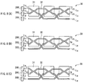
- FIG. 2 is a schematic configuration diagram of a crossing element.
- FIG. 4 is a conceptual diagram for explaining the action of the waveguide type optical switch of FIG. 3 .
- FIG. 5 is a schematic configuration diagram showing another example of the waveguide type optical switch.
- FIG. 6 is a conceptual diagram for explaining the action of the waveguide type optical switch of FIG. 5 .
- FIG. 10 is a conceptual diagram for explaining the action of the liquid crystal panel of FIG. 9 .
- FIG. 11 is a schematic configuration diagram of a liquid crystal projector according to a second embodiment of the invention.
- FIG. 18 is a waveform diagram for explaining the action of the diffraction type optical element of FIG. 16 .
- FIG. 20 is a schematic configuration diagram of an image display apparatus according to a sixth embodiment of the invention.
- FIG. 21 is a schematic configuration diagram of a liquid crystal projector according to a modification example.
- the three-color light source 10 is composed of a red laser 10 R, a green laser 10 G and a blue laser 10 B, and configured, for example, by parallel-arranging these lasers so that their respective optical axes are parallel to one another.
- the red laser 10 R is composed of, for example, an InAlGaP-based semiconductor laser
- the blue laser 10 B is composed of, for example, a GaN-based or an InGaN-based semiconductor laser.
- the green laser 10 G is composed of, for example, a solid-state laser excited by a semiconductor laser.
- the solid-state laser include solid-state lasers composed of YVO4+KTP (KTiOPO4), crystal PPLN (Periodically Poled LiNbO3), or PPMgO.LN (Periodically Poled MgO.LiNbO3).
- the waveguide type optical switch 30 is configured by optically connecting a plurality of crossing elements 31 with at least one of an optical fiber 32 and a mirror.
- a plurality of crossing elements 31 with at least one of an optical fiber 32 and a mirror.
- the crossing elements 31 as shown in FIGS. 2(A) and (B), two waveguides composed of, for example, LiNbO3 crystal (LN crystal) containing Ti are formed so as to intersect each other, and at least the end portions of individual waveguides are exposed to the surfaces of the crossing elements 31 .
- LN crystal LiNbO3 crystal
- a pair of electrodes are provided adjacent to a part of the two waveguides, and a voltage is applied to the pair of electrodes, and the resulting electric field is used to change the connection relationship between one end portions of individual waveguides (input terminals T 1 and T 2 ) and the other end portions (output terminals T 3 and T 4 ). That is, the crossing elements 31 function as optical switches to electrically switch the optical paths, so that the waveguide type optical switch 30 can arbitrarily switch the colors of color lights outputted to diffraction type optical elements 40 a , 40 b and 40 c (described later) in predetermined time intervals.
- the respective input terminals T 1 of the three crossing elements 31 (element (1, 1), element (2, 1) and element (3, 1)) of the three-color light source 10 side (the left side of FIG. 3 ) are arranged oppositely to the regions of the emitting side surfaces of the polarizing plates 20 R, 20 G and 20 B.
- the respective output terminals T 3 of the three crossing elements 31 (element (1, 3), element (2, 3) and element (3, 3)) of the diffraction type optical element 40 side are arranged oppositely to the incident side surface of the diffraction type optical element 40 .
- the green light L G and the blue light L B are outputted without changing the array, so that the red light L R is outputted to the diffraction type optical element 40 a , the green light L G is outputted to the diffraction type optical element 40 b , and the blue light L B is outputted to the diffraction type optical element 40 c.
- the red light L R inputted to the input terminal T 1 of the element (1, 1) is outputted from the output element T 3 of the element (2, 3)
- the green light L G inputted to the input terminal T 1 of the element (1, 2) is outputted from the output element T 3 of the element (3, 3)
- the blue light L B inputted to the input terminal T 1 of the element (1, 3) is outputted from the output element T 3 of the element (1, 3). That is, in this case, the color lights arrayed and inputted from above the paper surface of FIG.
- the green light L G and the blue light L B are outputted by switching the array from above the paper surface of FIG. 4(C) in the following order of the green light L G , the blue light L B and the red light L R , so that the green light L G is outputted to the diffraction type optical element 40 a , the blue light L B is outputted to the diffraction type optical element 40 b , and the red light L R is outputted to the diffraction type optical element 40 c.
- three crossing elements 31 are arranged in an array of 1 ⁇ 3, thereby being capable of arbitrarily switching the colors of the color lights outputted to the individual diffraction type optical elements 40 a , 40 b and 40 c , as shown in FIGS. 8(A) to (C). Consequently, when the waveguide type optical switch 30 has the configuration as shown in FIG. 5 or FIG. 7 , the number of the crossing elements 31 can be reduced than when the waveguide type optical switch 30 has the configuration as shown in FIG. 3 .
- the diffraction type optical elements 40 a , 40 b and 40 c are constructed of, for example, a DOE (Diffractive Optical Element).
- the DOE is for diffracting, for example, the incident light at a large number of points on an output plane, and configured to form the cross-sectional shape of the emitted light into predetermined shape and dimension by overlapping the individual diffractive lights with each other on the output plane, and also irradiate the output plane so as to make a luminance distribution uniform.
- the DOE has the property being insensible to the beam shapes of the incident lights.
- the field lens 50 is for changing the individual color lights diffusion-formed through the diffraction type optical elements 40 a , 40 b and 40 c into parallel lights, and is commonly provided on the optical paths of the individual color lights. As described above, it is configured so that the individual color lights having different incident angles (the diffused lights) enter the field lens 50 , and therefore the individual color lights refractively transmitted through the field lens 50 (the parallel lights) enter the liquid crystal panel 60 at different incident angles.
- the incident angles of the individual color lights entering the liquid crystal panel 60 depend on the incident angles of the individual color lights entering the field lens 50 , and further the incident angles of the individual color lights entering the field lens 50 are changed depending upon which one of the diffraction type optical elements 40 a , 40 b and 40 c the individual color lights are allowed to enter. Consequently, by selecting through the waveguide type optical switch 30 the colors of the color lights admitted into the diffraction type optical elements 40 a , 40 b and 40 c , the incident angles of the individual color lights into the liquid crystal panel 60 can be switched arbitrarily.
- the microlens array 61 B is constructed by arranging in a matrix a plurality of microlenses 61 D at the incidence regions of the individual color lights made into the parallel lights by the field lens 50 .
- the microlens array 61 B is a curved lens formed by curing, for example, a transparent resin or the like, and is configured to refract the individual color lights made into the parallel lights by the field lens 50 , and then individually admit them into pixel openings 65 described later, as shown in FIG. 10(A) to (C).
- the transparent substrates 61 A and 61 C are composed of, for example, quartz so as to protect the microlens array 61 B from the exterior.
- Recesses having the reversed shape of the shape of the microlens 61 D are formed in a matrix in the surface adjacent to the microlens array 61 B of the transparent substrate 61 A, and the transparent substrate 61 A and the microlens array 61 B are contacted to each other, leaving no space therebetween.
- An opposed common electrode 64 formed of a transparent conductive material such as ITO (Indium Tin Oxide) is formed on the surface adjacent to the liquid crystal layer 62 of the transparent substrate 61 C.
- the pixel openings 65 are composed of ITO or the like, and constitutes one dot together with the opposed common electrode 64 arranged oppositely with the liquid crystal layer 62 in between. As described above, it is configured so that one color light among the individual color lights condensed by the microlens array 61 B enters each of the individual pixel openings 65 , and pixel signals in accordance with the colors of the color lights transmitting through the pixel openings 65 are applied to the respective pixel openings 65 .
- the projection lens 70 projects the color image lights modulated by the liquid crystal panel 60 onto the screen (not shown) provided outside of the liquid crystal projector 1 .
- the polarizing directions of the red light L R , the green light L G and the blue light L B emitted individually and independently from the three-color light source 10 are adjusted so as to match with the polarizing axis of the liquid crystal panel 60 by the polarizing plate 20 , and thereafter the optical paths of the individual color lights are periodically switched by the waveguide type optical switch 30 .
- it is capable of periodically admitting the individual color lights into the individual dots of the liquid crystal panel 60 , so that the 1 pixel full color (multicolor) display can be performed with one dot, and the number of pixels can be increased approximately three times that of the existing display mode in which the 1 pixel full color display has been performed with three adjacent dots.
- the number of pixels can be increased about three times that of the existing display mode in which the 1 pixel full color display has been performed with three adjacent dots, and no noise occurs during switching of the optical paths of the individual color lights, the reliability is improved, there is no fear that loss occurs, and it is easy to establish synchronization.
- the individual color lights (L R , L G , L B ) are irradiated all the times to the liquid crystal panel 60 , and hence there is no fear of color break that becomes the problem when the individual color lights are irradiated on a per-color basis and time-divisionally to the liquid crystal panel. Further, the light utilization efficiency is higher, and a bright display can be achieved with lower power consumption than the case of irradiating the individual color lights on a per-color basis and time-divisionally to the liquid crystal panel.
- the three-color switching light source 11 is configured to include three color lasers 11 A, 11 B and 11 C, and a controller (not shown) to control the light emissions of these three color lasers 11 A, 11 B and 11 C.
- these three color lasers 11 A, 11 B and 11 C are arranged in parallel so that their respective optical axes are parallel to one another.
- the present embodiment is configured to periodically emit the color lights having different colors from the individual three-color lasers 11 A, 11 B and 11 C, and hence the color lights entering the individual diffraction type optical elements 40 a , 40 b and 40 c can be periodically switched as in the case of switching the optical paths of the individual color lights by using the waveguide type optical switch 30 .
- This enables periodic switching of the incident angles of the individual color lights diffusion-formed by the diffraction type optical elements 40 a , 40 b and 40 c into the field lens 50 , and thus the incident angles of the individual color lights into the liquid crystal panel 60 .
- FIG. 13 shows the schematic configuration of a liquid crystal projector 3 (a projection apparatus) according to a third embodiment of the invention.
- the liquid crystal projector 3 is different from the liquid crystal projector 2 of the second embodiment in the point that it includes a three switching light source array 12 , a polarizing plate array 21 and a diffraction type optical element array 41 as the backlight of the liquid crystal panel 60 .
- the difference from the second embodiment will be mainly described, and the descriptions of the configuration, the action and the effect common to the second embodiment are omitted suitably.
- the polarizing plate array 21 is configured by periodically arranging in a two-dimensional direction the polarizing plates 20 R, 20 G and 20 B of the first embodiment, and the polarizing plates 20 R, 20 G and 20 B are arranged individually on the optical paths of the individual color lights (beam lights) emitted from the red laser 10 R, the green laser 10 G and the blue laser 10 B.
- the red laser 10 R, the green laser 10 G and the blue laser 10 B which are arranged on the lower stage of the three-color switching light source array 11 are driven to emit red light, green light and blue light, respectively, in the array different from the previous period of time.
- the individual color lights emitted from the three-color switching light source array 11 transmit through the polarizing plate array 21 and are then diffusion-formed by the diffraction type optical element array 41 , and irradiated through the field lens 50 over the liquid crystal panel 60 .
- the present embodiment is configured to periodically emit the color lights having different colors from the three-color switching light source array 11 , and hence the color lights entering the individual diffraction type optical elements 40 a , 40 b and 40 c can be periodically switched as in the case of switching the optical paths of the individual color lights by using the waveguide type optical switch 30 .
- This enables periodic switching of the incident angles of the individual color lights diffusion-formed by the diffraction type optical elements 40 a , 40 b and 40 c into the field lens 50 , and thus the incident angle of the individual color lights into the liquid crystal panel 60 .
- the present embodiment uses the three-color switching light source array 11 configured to include the red laser 10 R, the green laser 10 G and the blue laser 10 B, thus eliminating the necessity for performing a color separation using dichroic mirrors.
- the apparatus can be minimized than the case of performing the color separation using the dichloic mirrors.
- FIG. 15 shows the schematic configuration of a liquid crystal projector 4 (a projection apparatus) according to a fourth embodiment of the invention.
- the liquid crystal projector 4 is different from the liquid crystal projector 1 of the first embodiment in the points that a beam expander 80 is provided between the three-color light source 10 and the polarizing plate 20 , and a diffraction type optical element 130 (an optical path switching section) is provided instead of the waveguide type optical switch 30 , and a refraction type optical element 140 (a diffusion forming section) is provided instead of the diffraction type optical element 40 .
- a beam expander 80 is provided between the three-color light source 10 and the polarizing plate 20
- a diffraction type optical element 130 an optical path switching section
- a refraction type optical element 140 a diffusion forming section
- the diffraction type optical element 130 is, as shown in FIG. 16 , configured by arranging a transparent substrate 131 , a liquid crystal layer 132 , a transparent substrate 133 , a liquid crystal layer 134 and a transparent substrate 135 in this order from the polarizing plate 20 side.
- Individual electrodes 136 R, 136 G and 136 B are formed on the surface of the transparent substrate 131 adjacent to the liquid crystal layer 132
- individual electrodes 137 R, 137 G and 137 B are formed on the surface of the transparent substrate 135 adjacent to the liquid crystal layer 134 .
- the transparent substrates 131 , 133 and 135 and the spacer 139 are composed of, for example, quartz or the like.
- the liquid crystal layers 132 and 134 are composed of polymer dispersed liquid crystal (PDLC).
- the polymer dispersed liquid crystal has liquid crystal dispersed regions 132 A and 134 A where liquid crystal is dispersed in a high concentration, and polymer regions 132 B and 143 B where polymer is dispersed in a high concentration.
- liquid crystal dispersed regions 132 A and 134 A have different orientations.
- the liquid crystal layer 132 and the liquid crystal layer 134 have different directions of refraction upon application of a voltage.
- the individual color lights entered into the diffraction type optical element 130 are, for example, as shown in FIG. 18(A) in a period of time ⁇ 1 , and are as shown in FIG. 18(B) in a period of time ⁇ 2 , and are as shown in FIG. 18(C) in a period of time ⁇ 3 .
- Vr 1 is zero volt
- Vr 2 is Vpr (>0) volt
- Vg 1 and Vg 2 are Vpg (>0) volt
- Vb 1 is Vpb (>0) volt
- Vb 2 is zero volt
- Vr 1 and Vr 2 are Vpr volt
- Vg 1 is Vpg volt
- Vg 2 is zero volt
- Vb 1 is zero volt
- Vb 2 is Vpb volt.
- Vr 1 is Vpr volt
- Vr 2 is zero volt
- Vg 1 is zero volt
- Vg 2 is Vpg volt
- Vb 1 and Vb 2 are Vpb volt.
- the individual color lights do not diffract and transmit linearly.
- the individual color lights are diffracted and transmitted, for example, upward on the paper surfaces of FIGS. 18(A) to (C).
- the individual color lights are diffracted and transmitted, for example, downward on the paper surfaces of FIGS. 18(A) to (C).
- the refraction type optical element 140 is configured by commonly providing on the optical paths of the individual color lights (the beam lights) outputted from the diffraction type optical element 130 .
- the refraction type optical element 140 is configured to perform diffusion forming of the individual color lights outputted from the diffraction type optical element 130 so as to expand throughout the entire display region (not shown) of the liquid crystal panel 60 .
- the refraction type optical element 140 converts the individual color lights (the beam lights) entered at different angles to the surface adjacent to the diffraction type optical element 130 , into diffused lights, and admit these diffused lights into the field lens 50 at different incident angles.
- the diffraction type optical element 130 is used to periodically switch the incident angles of the individual color lights into the liquid crystal panel 60 .
- the diffraction type optical element 130 functions as the optical switch for electrically switching the emission directions (the optical paths) of the individual color lights, and hence any noise as in mechanically rotating optical components, such as a galvano-mirror and a step mirror, does not occur at all during switching of the emission direction (the optical path).
- mechanically rotating optical components such as a galvano-mirror and a step mirror
- liquid crystal panel 60 as the light valve has been described in the embodiments and the like, it is of course possible to use a display panel utilizing other principle as a light valve.
- the diffraction type optical element 130 is configured to include the liquid crystal layer 132 and the liquid crystal layer 134 composed of polymer dispersed liquid crystal, it may be configured by other diffraction type optical element, for example, and an acoustic optical element (an AO element).
Landscapes
- Physics & Mathematics (AREA)
- General Physics & Mathematics (AREA)
- Optics & Photonics (AREA)
- Engineering & Computer Science (AREA)
- Multimedia (AREA)
- Signal Processing (AREA)
- Nonlinear Science (AREA)
- Liquid Crystal (AREA)
- Projection Apparatus (AREA)
- Transforming Electric Information Into Light Information (AREA)
Abstract
Description
Claims (14)
Applications Claiming Priority (3)
| Application Number | Priority Date | Filing Date | Title |
|---|---|---|---|
| JP2006-236218 | 2006-08-31 | ||
| JP2006236218A JP5200349B2 (en) | 2006-08-31 | 2006-08-31 | Projection device and image display device |
| PCT/JP2007/065949 WO2008026452A1 (en) | 2006-08-31 | 2007-08-16 | Projection device and image display device |
Publications (2)
| Publication Number | Publication Date |
|---|---|
| US20090323030A1 US20090323030A1 (en) | 2009-12-31 |
| US8042950B2 true US8042950B2 (en) | 2011-10-25 |
Family
ID=39135735
Family Applications (1)
| Application Number | Title | Priority Date | Filing Date |
|---|---|---|---|
| US12/309,924 Expired - Fee Related US8042950B2 (en) | 2006-08-31 | 2007-08-16 | Projection apparatus and image display apparatus with individual color light diffusion and microlens array |
Country Status (7)
| Country | Link |
|---|---|
| US (1) | US8042950B2 (en) |
| EP (1) | EP2058701A4 (en) |
| JP (1) | JP5200349B2 (en) |
| KR (1) | KR20090049589A (en) |
| CN (1) | CN101512431B (en) |
| TW (1) | TW200825610A (en) |
| WO (1) | WO2008026452A1 (en) |
Cited By (1)
| Publication number | Priority date | Publication date | Assignee | Title |
|---|---|---|---|---|
| US11112684B2 (en) * | 2018-11-30 | 2021-09-07 | Coretronic Corporation | Projection apparatus with illumination system having plurality of laser modules |
Families Citing this family (25)
| Publication number | Priority date | Publication date | Assignee | Title |
|---|---|---|---|---|
| JP5493483B2 (en) * | 2008-07-24 | 2014-05-14 | セイコーエプソン株式会社 | projector |
| JP5262850B2 (en) * | 2009-03-06 | 2013-08-14 | セイコーエプソン株式会社 | projector |
| US20100309391A1 (en) * | 2009-06-03 | 2010-12-09 | Honeywood Technologies, Llc | Multi-source projection-type display |
| JP5428822B2 (en) * | 2009-12-14 | 2014-02-26 | セイコーエプソン株式会社 | Lighting device and projector |
| JP2011128205A (en) * | 2009-12-15 | 2011-06-30 | Seiko Epson Corp | Image display device |
| CN106406001B (en) * | 2010-08-16 | 2019-09-20 | 深圳光峰科技股份有限公司 | Light source and its optical projection system of application |
| EP3623874B1 (en) | 2010-09-08 | 2021-11-10 | Dai Nippon Printing Co., Ltd. | Illumination device, projection apparatus and projection-type image display apparatus |
| TWI486700B (en) * | 2011-09-23 | 2015-06-01 | Appotronics Corp Ltd | Light source and projection system using the same |
| KR101441785B1 (en) * | 2013-01-11 | 2014-09-22 | 건양대학교산학협력단 | A 3-dimensional imaging system based on a stereo hologram |
| KR102062261B1 (en) * | 2013-08-08 | 2020-02-20 | 한국전자통신연구원 | An active diffuser for reducing speckle, and a laser display device having the active diffuser |
| CN104423091A (en) * | 2013-08-27 | 2015-03-18 | 鸿富锦精密工业(深圳)有限公司 | Backlight module and liquid crystal display device |
| JP5725138B2 (en) * | 2013-12-02 | 2015-05-27 | セイコーエプソン株式会社 | Lighting device and projector |
| US9529196B1 (en) | 2014-06-05 | 2016-12-27 | Iphysicist Ltd. | Image guide optics for near eye displays |
| JP6620534B2 (en) * | 2015-03-25 | 2019-12-18 | 株式会社Jvcケンウッド | Display device |
| KR101741912B1 (en) * | 2015-10-20 | 2017-06-16 | 한국기술교육대학교 산학협력단 | Image magnifier |
| CN106569382B (en) * | 2016-10-26 | 2018-07-06 | 深圳奥比中光科技有限公司 | Laser-projector and its depth camera |
| JP6744041B2 (en) * | 2017-03-23 | 2020-08-19 | Necディスプレイソリューションズ株式会社 | Light source device, projector and speckle reduction method |
| CN108803217B (en) * | 2017-05-04 | 2024-05-03 | 深圳光峰科技股份有限公司 | Excitation light source system and projection device |
| JP7068639B2 (en) * | 2017-07-05 | 2022-05-17 | 大日本印刷株式会社 | Direction display device |
| JP7090238B2 (en) * | 2018-04-27 | 2022-06-24 | 日亜化学工業株式会社 | Light source module |
| JP7132748B2 (en) * | 2018-05-24 | 2022-09-07 | スタンレー電気株式会社 | lighting equipment, light projection system |
| JP7400730B2 (en) * | 2018-11-29 | 2023-12-19 | ソニーグループ株式会社 | video projection device |
| CN110493504B (en) * | 2019-08-29 | 2021-07-30 | Oppo广东移动通信有限公司 | Image sensor, imaging system and terminal |
| CN114647137A (en) * | 2020-12-18 | 2022-06-21 | 深圳光峰科技股份有限公司 | Optical modulator and projection display system |
| DE102022106271A1 (en) | 2022-03-17 | 2023-09-21 | Ams-Osram International Gmbh | OPTOELECTRONIC MODULE AND METHOD FOR OPERATING AN OPTOELECTRONIC MODULE |
Citations (11)
| Publication number | Priority date | Publication date | Assignee | Title |
|---|---|---|---|---|
| JP2000105362A (en) | 1998-09-29 | 2000-04-11 | Seiko Epson Corp | Color image display system, image display device and light irradiation device |
| JP2002156617A (en) | 2000-11-20 | 2002-05-31 | Ricoh Co Ltd | Image display device |
| JP2002202414A (en) | 2000-10-26 | 2002-07-19 | Ricoh Co Ltd | Beam transducer element, illumination optical system using the beam transducer element, aligner, laser processing machine and projection device |
| US20030151785A1 (en) * | 1999-02-23 | 2003-08-14 | Victor Vertoprakhov | Holographic display apparatus and method |
| JP2004029784A (en) | 2002-06-20 | 2004-01-29 | Samsung Electronics Co Ltd | Image display device provided with optical scanner |
| JP2004264776A (en) | 2003-03-04 | 2004-09-24 | Seiko Epson Corp | Projector and optical device |
| US6836365B2 (en) * | 1999-04-15 | 2004-12-28 | Nikon Corporation | Diffractive optical element, method of fabricating the element, illumination device provided with the element, projection exposure apparatus, exposure method, optical homogenizer, and method of fabricating the optical homogenizer |
| JP2005173562A (en) | 2003-10-28 | 2005-06-30 | Sony Corp | Optical waveguide device, device for displaying image using optical waveguide device and method for displaying image |
| JP2005202068A (en) | 2004-01-14 | 2005-07-28 | Sony Corp | Deflection element and image display device using the same |
| JP2005202069A (en) | 2004-01-14 | 2005-07-28 | Sony Corp | Deflection element and image display device using the same |
| US7746559B2 (en) * | 2003-01-08 | 2010-06-29 | Explay Ltd. | Image projecting device and method |
Family Cites Families (6)
| Publication number | Priority date | Publication date | Assignee | Title |
|---|---|---|---|---|
| JPS5917511A (en) * | 1982-07-20 | 1984-01-28 | Fujitsu Ltd | Optical switch |
| JPH065350B2 (en) * | 1986-07-04 | 1994-01-19 | 沖電気工業株式会社 | Total reflection type optical switch |
| JP2503558B2 (en) * | 1987-12-29 | 1996-06-05 | 日本電気株式会社 | Optical switch |
| WO1994022050A1 (en) * | 1993-03-23 | 1994-09-29 | Optica Nova Onab Ab | Tv-projector |
| JP2003302599A (en) * | 2002-04-12 | 2003-10-24 | Sony Corp | Video projection device |
| KR100468167B1 (en) * | 2002-04-23 | 2005-01-26 | 삼성전자주식회사 | Apparatus for projection image |
-
2006
- 2006-08-31 JP JP2006236218A patent/JP5200349B2/en not_active Expired - Fee Related
-
2007
- 2007-08-16 US US12/309,924 patent/US8042950B2/en not_active Expired - Fee Related
- 2007-08-16 CN CN200780032575XA patent/CN101512431B/en not_active Expired - Fee Related
- 2007-08-16 EP EP07792582A patent/EP2058701A4/en not_active Withdrawn
- 2007-08-16 KR KR1020097003370A patent/KR20090049589A/en not_active Application Discontinuation
- 2007-08-16 WO PCT/JP2007/065949 patent/WO2008026452A1/en active Application Filing
- 2007-08-17 TW TW096130624A patent/TW200825610A/en not_active IP Right Cessation
Patent Citations (11)
| Publication number | Priority date | Publication date | Assignee | Title |
|---|---|---|---|---|
| JP2000105362A (en) | 1998-09-29 | 2000-04-11 | Seiko Epson Corp | Color image display system, image display device and light irradiation device |
| US20030151785A1 (en) * | 1999-02-23 | 2003-08-14 | Victor Vertoprakhov | Holographic display apparatus and method |
| US6836365B2 (en) * | 1999-04-15 | 2004-12-28 | Nikon Corporation | Diffractive optical element, method of fabricating the element, illumination device provided with the element, projection exposure apparatus, exposure method, optical homogenizer, and method of fabricating the optical homogenizer |
| JP2002202414A (en) | 2000-10-26 | 2002-07-19 | Ricoh Co Ltd | Beam transducer element, illumination optical system using the beam transducer element, aligner, laser processing machine and projection device |
| JP2002156617A (en) | 2000-11-20 | 2002-05-31 | Ricoh Co Ltd | Image display device |
| JP2004029784A (en) | 2002-06-20 | 2004-01-29 | Samsung Electronics Co Ltd | Image display device provided with optical scanner |
| US7746559B2 (en) * | 2003-01-08 | 2010-06-29 | Explay Ltd. | Image projecting device and method |
| JP2004264776A (en) | 2003-03-04 | 2004-09-24 | Seiko Epson Corp | Projector and optical device |
| JP2005173562A (en) | 2003-10-28 | 2005-06-30 | Sony Corp | Optical waveguide device, device for displaying image using optical waveguide device and method for displaying image |
| JP2005202068A (en) | 2004-01-14 | 2005-07-28 | Sony Corp | Deflection element and image display device using the same |
| JP2005202069A (en) | 2004-01-14 | 2005-07-28 | Sony Corp | Deflection element and image display device using the same |
Non-Patent Citations (2)
| Title |
|---|
| English Language Translation of Japanese Office Action issued May 10, 2011 for Japanese Application No. 2006-236218. |
| International Search Report; International Application No. PCT/JP2007/065949; Date: Sep. 11, 2007. |
Cited By (1)
| Publication number | Priority date | Publication date | Assignee | Title |
|---|---|---|---|---|
| US11112684B2 (en) * | 2018-11-30 | 2021-09-07 | Coretronic Corporation | Projection apparatus with illumination system having plurality of laser modules |
Also Published As
| Publication number | Publication date |
|---|---|
| TWI360718B (en) | 2012-03-21 |
| JP2008058665A (en) | 2008-03-13 |
| CN101512431B (en) | 2011-05-04 |
| KR20090049589A (en) | 2009-05-18 |
| WO2008026452A1 (en) | 2008-03-06 |
| US20090323030A1 (en) | 2009-12-31 |
| CN101512431A (en) | 2009-08-19 |
| EP2058701A1 (en) | 2009-05-13 |
| JP5200349B2 (en) | 2013-06-05 |
| TW200825610A (en) | 2008-06-16 |
| EP2058701A4 (en) | 2013-01-16 |
Similar Documents
| Publication | Publication Date | Title |
|---|---|---|
| US8042950B2 (en) | Projection apparatus and image display apparatus with individual color light diffusion and microlens array | |
| US8334937B2 (en) | Liquid crystal projector and image reproducing device | |
| US7746559B2 (en) | Image projecting device and method | |
| EP2023200A1 (en) | Reflective liquid crystal projector and image reproducing apparatus | |
| US20100177253A1 (en) | Coherent imaging method of laser projection and apparatus thereof | |
| US8425043B2 (en) | Projector having a plurality of optical devices with a purality of optical modulators | |
| JP2008277279A (en) | Planar lighting device and liquid crystal display using it | |
| KR20030010321A (en) | Single panel type image display apparatus | |
| JP2007066555A (en) | Surface light source and liquid crystal display device | |
| WO2016181771A1 (en) | Liquid crystal display device | |
| JP2001249400A (en) | Projection-type display apparatus | |
| CN113534587B (en) | Laser and projection apparatus | |
| US10901138B2 (en) | Light source device and display apparatus provided therewith | |
| CN113448159A (en) | Laser light source device and projection system | |
| JP2000206464A (en) | Illuminator, and projection type display device using the same | |
| JP2007163702A (en) | Speckle canceler and projector using it | |
| US6902276B2 (en) | Color projector apparatus and method | |
| CN218099913U (en) | Projection equipment and projection system | |
| KR100832621B1 (en) | Mobile projector which scans both forward path and backward path | |
| JP5157542B2 (en) | Projection type liquid crystal display device and electronic apparatus | |
| CN218213763U (en) | Projection equipment | |
| JP2010122242A (en) | Illumination device and image display apparatus using the same | |
| JP2006502434A (en) | Transmission projection system | |
| JPH10111535A (en) | Liquid crystal projector | |
| CN115421351A (en) | Projection equipment and projection system |
Legal Events
| Date | Code | Title | Description |
|---|---|---|---|
| AS | Assignment |
Owner name: SONY CORPORATION, JAPAN Free format text: ASSIGNMENT OF ASSIGNORS INTEREST;ASSIGNORS:HAZAMA, YOSHIKAZU;KAISE, KIKUO;REEL/FRAME:022241/0021 Effective date: 20081219 |
|
| ZAAA | Notice of allowance and fees due |
Free format text: ORIGINAL CODE: NOA |
|
| ZAAB | Notice of allowance mailed |
Free format text: ORIGINAL CODE: MN/=. |
|
| STCF | Information on status: patent grant |
Free format text: PATENTED CASE |
|
| FEPP | Fee payment procedure |
Free format text: PAYOR NUMBER ASSIGNED (ORIGINAL EVENT CODE: ASPN); ENTITY STATUS OF PATENT OWNER: LARGE ENTITY |
|
| FPAY | Fee payment |
Year of fee payment: 4 |
|
| MAFP | Maintenance fee payment |
Free format text: PAYMENT OF MAINTENANCE FEE, 8TH YEAR, LARGE ENTITY (ORIGINAL EVENT CODE: M1552); ENTITY STATUS OF PATENT OWNER: LARGE ENTITY Year of fee payment: 8 |
|
| FEPP | Fee payment procedure |
Free format text: MAINTENANCE FEE REMINDER MAILED (ORIGINAL EVENT CODE: REM.); ENTITY STATUS OF PATENT OWNER: LARGE ENTITY |
|
| LAPS | Lapse for failure to pay maintenance fees |
Free format text: PATENT EXPIRED FOR FAILURE TO PAY MAINTENANCE FEES (ORIGINAL EVENT CODE: EXP.); ENTITY STATUS OF PATENT OWNER: LARGE ENTITY |
|
| STCH | Information on status: patent discontinuation |
Free format text: PATENT EXPIRED DUE TO NONPAYMENT OF MAINTENANCE FEES UNDER 37 CFR 1.362 |
|
| FP | Lapsed due to failure to pay maintenance fee |
Effective date: 20231025 |