US8036248B2 - Method, apparatus, and system for automatic data aligner for multiple serial receivers - Google Patents
Method, apparatus, and system for automatic data aligner for multiple serial receivers Download PDFInfo
- Publication number
- US8036248B2 US8036248B2 US12/260,970 US26097008A US8036248B2 US 8036248 B2 US8036248 B2 US 8036248B2 US 26097008 A US26097008 A US 26097008A US 8036248 B2 US8036248 B2 US 8036248B2
- Authority
- US
- United States
- Prior art keywords
- data
- aligner
- ports
- port
- frame
- Prior art date
- Legal status (The legal status is an assumption and is not a legal conclusion. Google has not performed a legal analysis and makes no representation as to the accuracy of the status listed.)
- Active, expires
Links
Images


Classifications
-
- H—ELECTRICITY
- H03—ELECTRONIC CIRCUITRY
- H03M—CODING; DECODING; CODE CONVERSION IN GENERAL
- H03M9/00—Parallel/series conversion or vice versa
-
- G—PHYSICS
- G06—COMPUTING; CALCULATING OR COUNTING
- G06F—ELECTRIC DIGITAL DATA PROCESSING
- G06F13/00—Interconnection of, or transfer of information or other signals between, memories, input/output devices or central processing units
- G06F13/14—Handling requests for interconnection or transfer
-
- G—PHYSICS
- G06—COMPUTING; CALCULATING OR COUNTING
- G06F—ELECTRIC DIGITAL DATA PROCESSING
- G06F13/00—Interconnection of, or transfer of information or other signals between, memories, input/output devices or central processing units
- G06F13/38—Information transfer, e.g. on bus
-
- G—PHYSICS
- G06—COMPUTING; CALCULATING OR COUNTING
- G06F—ELECTRIC DIGITAL DATA PROCESSING
- G06F13/00—Interconnection of, or transfer of information or other signals between, memories, input/output devices or central processing units
- G06F13/38—Information transfer, e.g. on bus
- G06F13/42—Bus transfer protocol, e.g. handshake; Synchronisation
- G06F13/4282—Bus transfer protocol, e.g. handshake; Synchronisation on a serial bus, e.g. I2C bus, SPI bus
- G06F13/4295—Bus transfer protocol, e.g. handshake; Synchronisation on a serial bus, e.g. I2C bus, SPI bus using an embedded synchronisation
-
- G—PHYSICS
- G11—INFORMATION STORAGE
- G11C—STATIC STORES
- G11C7/00—Arrangements for writing information into, or reading information out from, a digital store
- G11C7/10—Input/output [I/O] data interface arrangements, e.g. I/O data control circuits, I/O data buffers
-
- G—PHYSICS
- G11—INFORMATION STORAGE
- G11C—STATIC STORES
- G11C7/00—Arrangements for writing information into, or reading information out from, a digital store
- G11C7/10—Input/output [I/O] data interface arrangements, e.g. I/O data control circuits, I/O data buffers
- G11C7/1006—Data managing, e.g. manipulating data before writing or reading out, data bus switches or control circuits therefor
-
- H—ELECTRICITY
- H04—ELECTRIC COMMUNICATION TECHNIQUE
- H04L—TRANSMISSION OF DIGITAL INFORMATION, e.g. TELEGRAPHIC COMMUNICATION
- H04L25/00—Baseband systems
- H04L25/02—Details ; arrangements for supplying electrical power along data transmission lines
- H04L25/14—Channel dividing arrangements, i.e. in which a single bit stream is divided between several baseband channels and reassembled at the receiver
-
- H—ELECTRICITY
- H04—ELECTRIC COMMUNICATION TECHNIQUE
- H04L—TRANSMISSION OF DIGITAL INFORMATION, e.g. TELEGRAPHIC COMMUNICATION
- H04L65/00—Network arrangements, protocols or services for supporting real-time applications in data packet communication
-
- H—ELECTRICITY
- H04—ELECTRIC COMMUNICATION TECHNIQUE
- H04L—TRANSMISSION OF DIGITAL INFORMATION, e.g. TELEGRAPHIC COMMUNICATION
- H04L7/00—Arrangements for synchronising receiver with transmitter
- H04L7/04—Speed or phase control by synchronisation signals
-
- Y—GENERAL TAGGING OF NEW TECHNOLOGICAL DEVELOPMENTS; GENERAL TAGGING OF CROSS-SECTIONAL TECHNOLOGIES SPANNING OVER SEVERAL SECTIONS OF THE IPC; TECHNICAL SUBJECTS COVERED BY FORMER USPC CROSS-REFERENCE ART COLLECTIONS [XRACs] AND DIGESTS
- Y02—TECHNOLOGIES OR APPLICATIONS FOR MITIGATION OR ADAPTATION AGAINST CLIMATE CHANGE
- Y02D—CLIMATE CHANGE MITIGATION TECHNOLOGIES IN INFORMATION AND COMMUNICATION TECHNOLOGIES [ICT], I.E. INFORMATION AND COMMUNICATION TECHNOLOGIES AIMING AT THE REDUCTION OF THEIR OWN ENERGY USE
- Y02D10/00—Energy efficient computing, e.g. low power processors, power management or thermal management
Definitions
- Embodiments of the invention generally relate to the field of networks and, more particularly, to automatic data aligner for multiple serial receivers in serial link technologies.
- Serial Port Memory Technology uses high speed serial link technology even in memory area. This serial link provides several benefits including low power and reduced pin counts and connects between host and memory. Although one serial link can support several Gbps of bandwidth, if memory bandwidth requirement gets higher than that supported by a single serial line, multiples serial links must be used to support the additional bandwidth requirement.
- a command 108 is encoded in multiple bits 110 and is sent bit by bit via a high speed link 102 as indicated by a second signal serial data 102 .
- this serialized data 102 arrive at the receiver side, these data bits 110 are parallelized again and stored in a bit packet, such as a 20-bit packet 112 as indicated by a third signal deserialized data 104 .
- this “deserialized” 20-bit data 104 cannot be used to decode because the command 108 can start in the middle of this received data.
- the deserialized data 104 at the receiver side is received as “fghabcde” 116 even though the host sent “abcdefgh” 118 .
- the starting position (or header) of the command 108 is needed to be identified, while the host data 100 is sent by the host in a predefined pattern.
- the predefined pattern is set to “abcdefgh” 118 .
- the correct command 114 is obtained by shifting two adjacent deserialized data 104 . This technique is referred to as “frame aligning”, and the predefined pattern 118 used for this aligning is referred to as “SYNC” character.
- a host If, however, a host has to send a large amount of data, the data is to be transferred via multiple serial links 152 - 162 as referenced in FIG. 1B that illustrates conventional frame and port aligning. Properties of multiple high speed links are different from each other.
- a sampling front-end block e.g., clock data recovery (CDR)
- CDR clock data recovery
- flight times from the host to the receiver for each channel are not exactly the same. For example, the host sends a set of data at the same time, while one receiver samples data at a first clock and the other receiver samples it at a second clock.
- FIG. 2 illustrates a method to measure path differences and make the necessary data alignment with respect to various channels for computer expansion cards.
- data is sent within a data stream at processing block 202 , and the host inserts two COMMA patterns into the data stream at processing block 204 and sends the data at processing block 206 .
- a receiver probes this pattern at processing block 208 , it checks the arrival time of the COMMA character on each channel or port at processing block 210 . It further determines whether the same COMMA character appeared earlier at another channel at decision block 212 . If yes, and there is a channel which does not yet have the COMMA character, the receiver inserts a one cycle delay for the data flowing through that channel at processing block 214 . If not, the process continues with the delay.
- FIG. 3 illustrates a conventional architecture 300 for providing virtual lane alignment (e.g. frame aligning and port aligning).
- a Clock Data Recovery (CDR) block that extracts clock (rck) from the incoming data to minimize the sampling error.
- CDR Clock Data Recovery
- the first component of the aligner block is a deserializer 302 that combines five sequential incoming 4-bit data to 20-bit data using a depth of five shift registers 308 .
- the second component is a frame aligner 304 to make the output start at a correct position.
- the deserializer 302 is running at a recovered clock (rck) and the frame aligner 304 is running at a system clock (clk)
- two registers of the five registers 308 are located to resolve the problem while crossing the clock domain.
- the combination may contain a register and a shifter.
- the third component is a port aligner 306 . If a one cycle delay is required, the output from a register located in the port aligner 306 is selected instead of the data coming from the frame aligner 304 .
- the aligning of data (e.g., frame aligning, port aligning), or compensating skew between multiple channels, is commonly used in various serial link technologies, such as PCI-Express.
- SPMT has rather short interconnection between host and memory compared to other serial technologies, and it means that data skew on channels could be limited in relatively short amount. The difference comes out to be 0 or 1 in host clock cycle. It uses one kind of SYNC character to set up the outgoing and incoming channels and does not send distinguishable or special character to measure data skew.
- FIFO First In First Out
- a method, apparatus and system are provided for employing an automatic data aligner for multiple serial receivers in serial link technologies (e.g., computer expansion cards).
- serial link technologies e.g., computer expansion cards
- a method includes converting a transmission data path of a single bit into a parallel bit via a data aligner, wherein the data is being transmitted via one or more ports, and binding data transmission channels to reduce latency in transmission of the data, wherein the binding of the data transmission channels further includes inserting delay to match latency via the one or more ports.
- an apparatus in one embodiment, includes a mechanism for data alignment for multiple serial receivers, the mechanism including a data aligner to convert a transmission data path of a single bit into a parallel bit via, wherein the data is being transmitted via one or more ports, and bind data transmission channels to reduce latency in transmission of the data, wherein the binding of the data transmission channels further includes inserting delay to match latency via the one or more ports.
- a system in one embodiment, includes a computer system having a processor and a memory coupled to the processor, the computer system having a mechanism for data alignment for multiple serial receivers, the mechanism including a data aligner to convert a transmission data path of a single bit into a parallel bit via a data aligner, wherein the data is being transmitted via one or more ports, and bind data transmission channels to reduce latency in transmission of the data, wherein the binding of the data transmission channels further includes inserting delay to match latency via the one or more ports.
- FIG. 1A illustrates conventional frame aligning
- FIG. 1B illustrates conventional frame and port aligning
- FIG. 2 illustrates conventional process to measure and compensate path difference
- FIG. 3 illustrates a conventional architecture 300 for providing virtual lane alignment
- FIG. 4 illustrates an embodiment of alignment architecture for providing an aligning system to reduce latency
- FIG. 5 illustrates an embodiment of a 4-to-20 aligner
- FIG. 6 illustrates an embodiment of a process for aligning using a 4-to-20 bit aligner
- FIG. 7 illustrates an embodiment of comparator array
- FIG. 8 illustrates an embodiment of data path
- FIG. 9 illustrates an embodiment of obtaining a frame aligned 20-bit data stream
- FIG. 10 illustrates an embodiment of control generator having an internal clock signal to avoid clock domain crossing problem
- FIG. 11 illustrates an embodiment of a relationship between latency and pointer in 4-to-20 port aligner
- FIG. 12 illustrates an embodiment of port alignment based on pointer value over multiple ports
- FIG. 13 illustrates an embodiment of a process associated with a jmp signal
- FIG. 14 illustrates an embodiment a process for performing automatic data alignment for multiple data transmission channels
- FIG. 15 illustrates a computer system on which an embodiment of the present invention may be implemented.
- Embodiments of the invention are generally directed to port multiplier enhancement.
- SPMT is regarded as a new memory interface architecture, initially targeted for Dynamic Random Access Memory (DRAM) chips, that employs a serial interface architecture as opposed to a parallel interface architecture as commonly found in current memory technologies.
- SPMT typically uses a high speed serial link technology even in a memory area, providing the benefits of low power and reduced pin counts when connecting between a host and a memory.
- memory bandwidth requirement gets higher than a high speed link can support (e.g., several Gbps)
- multiples serial links must be used. Therefore, when a host is to send a large amount of data (e.g., read-data, write-data) at once, the memory is to be provided with enough bandwidth to pass the large amount of data through the multiple serial links or serial channels.
- multiple links or channels are used physically, the passing data is treated as single large logical channel and is referred to as “port binding” because serial ports on host or memory are bounded to provide larger bandwidth.
- the embodiments of the present invention improve upon SPMT and provide for greater bandwidth flexibility, significantly reduced pin count, lower power demand and savings on overall system cost. This technique is particularly crucial to mobile devices to help increase functionality while maintaining or reducing overall system cost, because a type of memory system is often an essential consideration when designing a mobile device.
- any serialized data at the receiver side is to be aligned to a “frame-boundary” or “header”.
- each frame-aligned data is aligned to provide the same latency, referred to as “inter-channel alignment”.
- the frame-boundary and header are checked by a receiver using a SYNC pattern (e.g., K28.5 in 8B10B coding).
- the inter-channel alignment is performed outside of PHY layer, which is implemented using FIFO to handle long delays.
- the technique of port-binding refers to aligning the data from multiple channels at the receiver side having same latency (inter-channel alignment) such that the received data is to have the same data from one host. If a channel (or a serial link) has latency different from that of others, the received data is not considered aligned.
- the technique of aligning data, or compensating skew between multiple channels is commonly used in other serial link technologies, such as High-Definition Multimedia Interface (HDMI) and PCI-Express.
- HDMI High-Definition Multimedia Interface
- TMDS Transition Minimized Differential Signal
- RGB red green blue
- FIFO is placed after the PHY and the data on each channel and is aligned with a measuring position of the SYNC character.
- the data is aligned on multi-channels even if there is a large path difference over the channels.
- the technique to place the data on multiple channels is referred to as “data striping” and the two SYNC characters appear periodically to measure the data skew between the channels.
- SPMT has rather short interconnection between host and memory compared to other serial technologies, which means the data skew on channels is to be limited to a relatively short amount. The resulting difference is typically 0 or 1 in a host clock cycle.
- One kind of SYNC character is used to set up the outgoing and incoming channels and no distinguishable or special characters are sent to measure the data skew. This means the conventional bulky FIFO-based technique is not to be applied to compensate the data skew while the channel is in the setup period.
- FIG. 4 illustrates an embodiment of alignment architecture 400 for providing an aligning system to reduce latency.
- Alignment architecture 400 includes an aligner 402 , CDR 404 , a port aligner 406 , and deserializers 408 - 414 .
- various techniques are employed to reduce latency. For example, conventionally, it takes at least three cycles from a 4-bit CDR output to be prepared as an input to the shifter inside a frame aligner. Using the architecture 400 , this latency is minimized by reducing these three cycles to a single cycle.
- a 4-bit CDR output is put into a correct position using a single register (see FIG. 6 ) instead of using the shift registers as illustrated in FIG.
- a new working clock (e.g., rck 20 , sck 416 etc) is generated from and replaces the two clocks, rck and clk (e.g., 312 , 312 of FIG. 3 ), to eliminate any clock-domain crossing problems that are caused when the two clocks rck and clk are employed.
- clock cycles for frame aligning are cut from 4 cycles to 2 cycles.
- a small delay is inserted in an input stream of data instead of having a single cycle delay in a port aligner block.
- the target system is the underline memory and a path difference is maintained as a small amount because the host and the receiver are located in one board. Further, in this case, a determination is made as to whether there is a possibility that a cycle mismatch may occur on the receiver side while examining the pointer value used for frame aligning, which can help reduce an additional cycle.
- port aligning is performed without any special character (e.g. COMMA in PCI-Express).
- having removed a special character leads to (1) simplifying of the underline hardware while keeping the relevant protocol simple, and (2) reducing the time required to set up for a channel (e.g., training time). For example, within the “channel-setup-period” a start position of a data packet is detected and found. Further, the channel set-up period is to find frame-boundary or header as well as to align inter-channel data.
- a special character e.g., SYNC, COMMA
- synchronize of data is performed on multiple channels within the channel-setup-period without using a special character, while the data skew between multi-channels is maintained shorter than half of the typical host clock period. For example, a latency of 6 clock cycles resulting from using the conventional architecture may be reduced to merely 3 cycles using a novel technique according to one embodiment.
- the architecture 400 having an SPMT receiver PHY consisting of four ports of deserializer 408 - 414 assigned to each channel and one control block that controls the delay of channels.
- Each port 408 - 414 is associated with a CDR 404 to detect one-bit serial data on a differential pair (e.g., RX 0 416 ) with a given clock signals, pck 424 , to combine the data into a 4-bit data and passes it to 4-to-20 aligner 402 using a recovered clock signal (rck). Then, the 4-to-20 aligner 402 generates 20-bit data using the incoming 4-bit data stream, and detects the start-bit-position while the channel is in channel-setup-period or training time, and aligns the data with remembered position thereafter.
- the port aligner 406 is responsible for generating a signal that is given to the 4-to-20 aligner to perform its tasks.
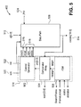
- FIG. 5 illustrates an embodiment of a 4-to-20 aligner 402 .
- the illustrated embodiment of the 4-to-20 aligner 402 provides various components and elements of the aligner 402 , such as a data path 508 and a control path 510 .
- the data path 508 contains various registers multiplexers, while the control path includes a control generator 502 , a comparator array 504 , and a finite state machine (FSM) 508 .
- the control path 510 and its components are to control the workings of the data path 508 by generating proper control signals for the data path 508 and interacting with external components and machines via the FSM 508 .
- FSM 508 provides interfacing with external components and machines.
- Control generator 502 passes control signals 516 along with rck 20 518 to data path 508 , and communicates an intermediate clock (e.g., rck 20 ) which has the same frequency to system clock (sck) 520 that is synchronized to recovered clock (rck) 522 .
- rck 20 system clock
- sck system clock
- rck recovered clock
- These signals 516 are used to align the data in a frame boundary.
- a control signal, jmp 524 is received from an external port aligner to make each port aligned altogether. This is discussed with respect to FIG. 10 .
- FIG. 6 illustrates an embodiment of a process for aligning using a 4-to-20 bit aligner.
- a 20-bit data stream is aligned using a 4-to-20 aligner by, for example, issuing a SearchFrame signal to run this aligner.
- FSM is to manage the aligner globally and communicate with external hardware.
- a decision is made as to whether a frame is to be aligned. If not, the process continues with returning to decision block 602 . If yes, the 4-to-20 bit aligner clears the pointer first and makes data path filled with new pointer value (e.g., setting the pointer to 0) at processing block 604 and waits 3 cycles to obtain the aligned 20-bit data at processing block 606 .
- new pointer value e.g., setting the pointer to 0
- the new aligned data with pointer ‘0’ is checked by a comparator array to detect whether the first 4-bit of SYNC pattern exists within the unaligned 20-bit data and calculate pointer values (e.g., ptr[4:0]/wptr[2:0]) with the found position of a 4-bit pattern. This represents the first half stage of the channel setup period.
- wptr values from each port are passed to a port aligner coupled to the 4-to-20 aligner block. By checking these values, the port aligner determined whether an 8 user interface (UI) delay is to be inserted into each port at processing block 610 .
- the port aligner block sends this instruction as a jmp signal to all components connected the 4-to-20 aligner. With this jmp signal and the already found header position, the comparator array to calculate a pointer value depending on the header position at processing block 612 . The pointer value is then stored at a register. Once the pointer is determined, it waits 3 cycles to make data path filled with the new pointer value at processing block 614 . This is considered the second half stage of the channel setup period.
- UI 8 user interface
- the aligned 20-bit data is placed as an output of data path (e.g., rxdata[19:0]) after the second half stage.
- the 4-to-20 aligner raises a signal (e.g., FrameLocked signal) to indicate that a frame boundary is found if the aligned 20-bit data is SYNC. If not, it runs the entire process again until the SYNC is found associated with the aligned 20-bit data.
- FIG. 7 illustrates an embodiment of comparator array 504 .
- comparator array 504 includes any number of comparators, such as twenty 4-bit comparators 702 (e.g., 4b cmp[0]-[19]) as illustrated.
- a 4-bit extractor 704 extracts twenty 4-bit sequential data streams from an incoming 20-bit data stream via a 4-bit extractor 704 and these twenty 4-bit extracted data streams are passed to corresponding comparators 702 .
- Each comparator compares each of the twenty incoming 4-bit data streams with a 4-bit constant 706 (e.g., 0010), which triggers the starting of a 4-bit SYNC character.
- One of these comparators may report ‘matching’ in a channel setup period.
- comparing results are then encoded into a 5-bit digit by a 20-to-5 bit encoder 708 and latched by an output register 710 if the set is one (e.g., setptr) 712 . Meanwhile, the upper 3 bits of an unlatched signal is passed as an output signal (e.g., wptr) 714 and is used by an external port aligner.
- an output signal e.g., wptr
- FIG. 8 illustrates an embodiment of data path 508 .
- data path 508 consists of five stages 810 - 818 .
- the first stage 810 includes inserting a two cycle delay depending on a jmp signal value 802 that is received from an external port aligner coupled with data path 508 , and inserts two rck cycles (or 8 UI) 820 when this is on. Functions of this stage are further discussed elsewhere in this document.
- the second stage 812 includes a shifter selecting a 4-bit data stream from an 8-bit input data stream that is combined with two sequential 4-bit data stream.
- the shifter includes an 8-to-4 shifter to replace a large conventional 40-to-20 shifter.
- the functions of this 8-to-4 shifter nay depend on a 2-bit msel signal value 804 .
- the third stage 814 of data path 508 includes placing or aligning finely shifted data in proper order.
- the related control signal 806 e.g., Iden
- Iden is properly generated to place the header of a received packet to be latched at the first register. In other words, data becomes aligned in two stages: once at the fine level and then again at the coarse level.
- the aligned data is selected and a one cycle delay is latched before it by using a number of multiplexers 808 (e.g., four illustrated multiplexers) is the fourth stage 816 .
- the fifth and final stage 818 contains merely two registers that are used to hold the aligned 20-bit data.
- the latency gets changed each time a jmp signal 802 is triggered. If the frame aligner does not need to perform frame aligning, the port aligner then performs port aligning instead. In such a situation, as detected by the port aligner, the jmp signal 802 is generated and a two cycle delay is inserted into the input data stream in the second stage 812 . Since this delay is performed in rck domain 820 , in one embodiment, the penalty is relatively small compared to the one imposed in a conventional system. Further, this may not be necessary when merely a single channel is employed. However, when data arrives on multiple channels, the data can be aligned with selecting a proper jmp value 802 . This is further described with respect to FIG. 12 .
- control generator 502 extract 20-bit data from a data stream, an intermediate clock having 20 UI clock periods is used and is generated by using clock rck 1004 .
- This clock signal is referred to as rck 20 1006 and generated in control generator 502 .
- the clock signal rck 20 1006 has a property to be about 180 degree phase difference from clock sck 1002 .
- Another role of control generator 502 is to generate control signals for data path 508 with a given pointer value (ptr) that comes from comparator array 504 (illustrated in FIG. 5 ).
- a tip to reduce power consumption is employed. For example, after a channel is set, comparator array is not needed and thus, the aligned 20-bit data stream is masked and passed to comparator array to reduce power consumption when a signal (e.g., framelocked signal) becomes on.
- a signal e.g., framelocked signal
- FIG. 11 illustrates an embodiment of a relationship between latency 1102 and pointer 1104 in 4-to-20 port aligner 402 .
- 4-to-20 port aligner 402 generates parallel data from high speed signal and passes the result to system clock domain.
- latency 1102 in system clock domain increases at certain positions, such as positions 1106 , 1108 , reflecting an increasing communication delay of high speed channel. Meanwhile, the delay on high speed channel affect location of a frame boundary, and this information can be obtained as pointer values of pointer 1104 .
- several essential points are detected, such each latency increase 1106 , 1108 reflecting a discontinuity point. In this case, latency 1102 increases at positions 1106 , 1108 (at ptr 8, wptr 2).
- FIG. 12 illustrates an embodiment of port alignment based on pointer values over multiple ports.
- the illustrated embodiment provides a relationship between latency 1202 and pointer 1204 (and wptr 1206 ) having various bars 1208 - 1220 reflecting various ptr values 1204 and wptr values 1206 being received from each port.
- first port 1222 of bar 1208 has a wptr value of 0, while second port 1224 of bar 1218 has a wptr value of 2, which indicates that the latencies for these two ports are different from each other.
- first port 1228 of bar 1210 is at wptr 1
- second port 1230 of bar 1220 is at wptr 3.
- the amount necessary to shift the two bars 1210 , 1220 to the two new wptr values in a safe zone may require two clocks of rck or 8 UI's 1232 .
- the remaining illustrations of case 3 1212 , case 4 1214 , and case 5 1216 are already placed in a safe zone and there is no need for shifting them.
- the pointer shift may be decided depending on wptr values from other ports even if one wptr has a value of 0.
- the jmp values equals 0 at block 1314 .
- the jmp value is set at 1 at block 1308 . If not, the jmp value is set at 0 at block 1314 .
- This decision may be calculated in a single cycle in parallel. It also raises an allstable signal, as shown in FIG. 5 , to indicate that jmp is decided and the connected 4-to-20 aligner is made aware of it.
- FIG. 14 illustrates an embodiment a process for performing automatic data alignment for multiple data transmission channels.
- a deserializer is turned on and is configured to detect a frame boundary and be ready for normal operation after it is turned on.
- a device is turned on and sends a SYNC2 pattern to a host at initial state.
- a host coupled with the device sends a SYNC pattern.
- the device asserts aligners (inside the device) to proceed with finding frame boundary (e.g., SearchFrame), and so the aligner seek to find a predefined sequence of SYNC patterns inside an incoming data stream at processing block 1408 .
- the aligners interact with port aligner to find the frame boundary and achieve synchronization between ports.
- FIG. 15 illustrates a computer system 1500 on which an embodiment of the present invention may be implemented.
- Computer system 1500 includes a system bus 1520 for communicating information, and a processor 1510 coupled to bus 1520 for processing information.
- processor 1510 is implemented using one of the multitudes of microprocessors. Nevertheless one of ordinary skill in the art will appreciate that other processors may be used.
- Computer system 1500 further comprises a random access memory (RAM) or other dynamic storage device 1525 (referred to herein as main memory), coupled to bus 1520 for storing information and instructions to be executed by processor 1510 .
- Main memory 1525 also may be used for storing temporary variables or other intermediate information during execution of instructions by processor 1510 .
- Computer system 1500 also may include a read only memory (ROM) and or other static storage device 1526 coupled to bus 1520 for storing static information and instructions used by processor 1510 .
- ROM read only memory
- a data storage device 1525 such as a magnetic disk or optical disc and its corresponding drive may also be coupled to computer system 1500 for storing information and instructions.
- Computer system 1500 can also be coupled to a second input/output (I/O) bus 1550 via an I/O interface 1530 .
- I/O input/output
- a plurality of I/O devices may be coupled to I/O bus 1550 , including a display device 1524 , an input device (e.g., an alphanumeric input device 1523 and or a cursor control device 1522 ).
- the communication device 1521 is for accessing other computers (servers or clients) via external data network.
- Computer system 1500 may be interconnected in a client/server network system.
- a network may include a Local Area Network (LAN), Wide Area Network (WAN), Metropolitan Area Network (MAN), intranet, the Internet, etc.
- LAN Local Area Network
- WAN Wide Area Network
- MAN Metropolitan Area Network
- any number of network devices can be cascaded into being connected with a port multiplier forming a networking mechanism within a network. It is contemplated that there may be any number of devices connected via the network.
- a device may transfer data streams, such as streaming media data, to other devices in the network system via a number of standard and non-standard protocols, including the protocols described in this document.
- Various embodiments of the present invention may include various processes. These processes may be performed by hardware components or may be embodied in computer program or machine-executable instructions, which may be used to cause a general-purpose or special-purpose processor or logic circuits programmed with the instructions to perform the processes. Alternatively, the processes may be performed by a combination of hardware and software.
- modules, components, or elements described throughout this document may include hardware, software, and/or a combination thereof.
- a module includes software
- the software data, instructions, and/or configuration may be provided via an article of manufacture by a machine/electronic device/hardware.
- An article of manufacture may include a machine accessible/readable medium having content to provide instructions, data, etc. The content may result in an electronic device, for example, a filer, a disk, or a disk controller as described herein, performing various operations or executions described.
- Portions of various embodiments of the present invention may be provided as a computer program product, which may include a computer-readable medium having stored thereon computer program instructions, which may be used to program a computer (or other electronic devices) to perform a process according to the embodiments of the present invention.
- the machine-readable medium may include, but is not limited to, floppy diskettes, optical disks, compact disk read-only memory (CD-ROM), and magneto-optical disks, read-only memory (ROM), random access memory (RAM), erasable programmable read-only memory (EPROM), electrically EPROM (EEPROM), magnet or optical cards, flash memory, or other type of media/machine-readable medium suitable for storing electronic instructions.
- the present invention may also be downloaded as a computer program product, wherein the program may be transferred from a remote computer to a requesting computer.
- element A may be directly coupled to element B or be indirectly coupled through, for example, element C.
- a component, feature, structure, process, or characteristic A “causes” a component, feature, structure, process, or characteristic B, it means that “A” is at least a partial cause of “B” but that there may also be at least one other component, feature, structure, process, or characteristic that assists in causing “B.” If the specification indicates that a component, feature, structure, process, or characteristic “may”, “might”, or “could” be included, that particular component, feature, structure, process, or characteristic is not required to be included. If the specification or claim refers to “a” or “an” element, this does not mean there is only one of the described elements.
- An embodiment is an implementation or example of the present invention.
- Reference in the specification to “an embodiment,” “one embodiment,” “some embodiments,” or “other embodiments” means that a particular feature, structure, or characteristic described in connection with the embodiments is included in at least some embodiments, but not necessarily all embodiments.
- the various appearances of “an embodiment,” “one embodiment,” or “some embodiments” are not necessarily all referring to the same embodiments. It should be appreciated that in the foregoing description of exemplary embodiments of the present invention, various features are sometimes grouped together in a single embodiment, figure, or description thereof for the purpose of streamlining the disclosure and aiding in the understanding of one or more of the various inventive aspects.
Abstract
Description
Claims (18)
Priority Applications (8)
| Application Number | Priority Date | Filing Date | Title |
|---|---|---|---|
| US12/260,970 US8036248B2 (en) | 2008-10-29 | 2008-10-29 | Method, apparatus, and system for automatic data aligner for multiple serial receivers |
| EP09744823.7A EP2351303B8 (en) | 2008-10-29 | 2009-09-30 | Method, apparatus, and system for automatic data aligner for multiple serial receivers |
| PCT/US2009/059080 WO2010053637A2 (en) | 2008-10-29 | 2009-09-30 | Method, apparatus, and system for automatic data aligner for multiple serial receivers |
| KR1020117012260A KR101470989B1 (en) | 2008-10-29 | 2009-09-30 | Method, apparatus, and system for automatic data aligner for multiple serial receivers |
| CN200980144150.7A CN102204198B (en) | 2008-10-29 | 2009-09-30 | Method, apparatus, and system for automatic data aligner for multiple serial receivers |
| JP2011534572A JP5568089B2 (en) | 2008-10-29 | 2009-09-30 | Method, apparatus and system for automatic data aligner for multiple serial receivers |
| DE202009019093.5U DE202009019093U1 (en) | 2008-10-29 | 2009-09-30 | Device and system for automatic data aligners for multiple serial receivers |
| TW098133897A TWI502358B (en) | 2008-10-29 | 2009-10-06 | Method, apparatus, and system for automatic data aligner for multiple serial receivers |
Applications Claiming Priority (1)
| Application Number | Priority Date | Filing Date | Title |
|---|---|---|---|
| US12/260,970 US8036248B2 (en) | 2008-10-29 | 2008-10-29 | Method, apparatus, and system for automatic data aligner for multiple serial receivers |
Publications (2)
| Publication Number | Publication Date |
|---|---|
| US20100103929A1 US20100103929A1 (en) | 2010-04-29 |
| US8036248B2 true US8036248B2 (en) | 2011-10-11 |
Family
ID=42117442
Family Applications (1)
| Application Number | Title | Priority Date | Filing Date |
|---|---|---|---|
| US12/260,970 Active 2030-01-19 US8036248B2 (en) | 2008-10-29 | 2008-10-29 | Method, apparatus, and system for automatic data aligner for multiple serial receivers |
Country Status (8)
| Country | Link |
|---|---|
| US (1) | US8036248B2 (en) |
| EP (1) | EP2351303B8 (en) |
| JP (1) | JP5568089B2 (en) |
| KR (1) | KR101470989B1 (en) |
| CN (1) | CN102204198B (en) |
| DE (1) | DE202009019093U1 (en) |
| TW (1) | TWI502358B (en) |
| WO (1) | WO2010053637A2 (en) |
Cited By (2)
| Publication number | Priority date | Publication date | Assignee | Title |
|---|---|---|---|---|
| US9888077B2 (en) | 2014-04-22 | 2018-02-06 | Western Digital Technologies, Inc. | Metadata based data alignment in data storage systems |
| US10594892B2 (en) | 2017-05-18 | 2020-03-17 | Analog Devices Global | High speed serial link for video interfaces |
Families Citing this family (10)
| Publication number | Priority date | Publication date | Assignee | Title |
|---|---|---|---|---|
| CN102412900A (en) * | 2011-11-30 | 2012-04-11 | 中国航空工业集团公司第六三一研究所 | Method for realizing function of data bit realignment in fiber channel |
| CN102970109B (en) | 2012-11-16 | 2016-06-22 | 中兴通讯股份有限公司 | The data transmission method of a kind of high-speed multiple channel, relevant apparatus and system |
| CN103744827A (en) * | 2014-01-10 | 2014-04-23 | 浪潮电子信息产业股份有限公司 | Serial data frame matching method for improving chip logical time sequence |
| KR102225619B1 (en) * | 2015-02-10 | 2021-03-12 | 한화테크윈 주식회사 | High-speed serial data receiving apparatus |
| US10455501B2 (en) * | 2016-12-22 | 2019-10-22 | Macom Connectivity Solutions, Llc | Power optimization mechanisms for framers by serializing frame alignment processes for multiple lanes |
| US10313102B2 (en) * | 2016-12-22 | 2019-06-04 | Macom Connectivity Solutions, Llc | Power optimization mechanisms for framers by selectively deactivating frame alignment process |
| TWI678902B (en) * | 2018-11-28 | 2019-12-01 | 中華電信股份有限公司 | Network system for packet processing/exchange for applications and method thereof |
| WO2021111329A1 (en) * | 2019-12-02 | 2021-06-10 | Zixi, Llc | Packetized data communication over multiple unreliable channels |
| CN111431533B (en) * | 2020-04-26 | 2023-06-16 | 杭州电子科技大学富阳电子信息研究院有限公司 | Method for synchronizing ADC data and clock of high-speed LVDS interface |
| US11899609B2 (en) | 2021-12-20 | 2024-02-13 | Nvidia Corporation | Frame alignment recovery for a high-speed signaling interconnect |
Citations (18)
| Publication number | Priority date | Publication date | Assignee | Title |
|---|---|---|---|---|
| US5408473A (en) * | 1992-03-03 | 1995-04-18 | Digital Equipment Corporation | Method and apparatus for transmission of communication signals over two parallel channels |
| WO2001078337A1 (en) | 2000-04-11 | 2001-10-18 | Parthus Technologies Plc | Method and apparatus for multi-lane communication channel with deskewing capability |
| US6374386B1 (en) * | 1998-08-20 | 2002-04-16 | Samsung Electronics Co., Ltd. | Device and method for inserting previously known bits in input stage of channel encoder |
| US20020184412A1 (en) * | 2001-06-02 | 2002-12-05 | Stevens James Ray | System and method for locating and aligning to framing bits |
| US6690757B1 (en) | 2000-06-20 | 2004-02-10 | Hewlett-Packard Development Company, L.P. | High-speed interconnection adapter having automated lane de-skew |
| US20040117499A1 (en) * | 2002-12-13 | 2004-06-17 | Bo Liu | System and method for detection of delineation of data units for a communication element |
| US20040264496A1 (en) * | 1998-12-14 | 2004-12-30 | Shaffer Michael S. | Communications system with symmetrical interfaces and associated methods |
| US20050005051A1 (en) | 2003-07-02 | 2005-01-06 | Wayne Tseng | Circuit and method for aligning data transmitting timing of a plurality of lanes |
| US20050025195A1 (en) * | 2003-06-02 | 2005-02-03 | Pmc-Sierra, Inc. | Serial data validity monitor |
| US6970435B1 (en) * | 1998-06-15 | 2005-11-29 | International Business Machines Corporation | Data alignment compensator |
| US20060092969A1 (en) | 2000-09-13 | 2006-05-04 | Susnow Dean S | Multi-lane receiver de-skewing |
| US20060156083A1 (en) * | 2005-01-10 | 2006-07-13 | Samsung Electronics Co., Ltd | Method of compensating for a byte skew of PCI express and PCI express physical layer receiver for the same |
| US20060273941A1 (en) | 2005-06-02 | 2006-12-07 | Agere Systems, Inc. | Content deskewing for multichannel synchronization |
| US20070115974A1 (en) * | 2001-08-30 | 2007-05-24 | Messenger Brian S | High speed data classification system |
| WO2008026164A2 (en) | 2006-08-29 | 2008-03-06 | Koninklijke Philips Electronics N.V. | Method and apparatus for synchronization of a high speed lvds communication |
| US20080123638A1 (en) * | 2006-06-08 | 2008-05-29 | Jiann Liao | Efficient strip-sown and re-alignment of ingressing physical layer/data layer packets in an aggregated PCI-express port having eight lanes |
| US20080169946A1 (en) * | 2007-01-11 | 2008-07-17 | Samsung Electronics Co., Ltd. | Deserializer, related method, and clock frequency divider |
| US7558893B2 (en) * | 2004-09-23 | 2009-07-07 | International Business Machines Corporation | Latency optimized data alignment racheting scheme |
Family Cites Families (9)
| Publication number | Priority date | Publication date | Assignee | Title |
|---|---|---|---|---|
| JPS5827448A (en) * | 1981-08-10 | 1983-02-18 | Nippon Telegr & Teleph Corp <Ntt> | Broad band communication system |
| GB8407223D0 (en) * | 1984-03-20 | 1984-04-26 | British Telecomm | Broadband digital transmission systems |
| JPS6386630A (en) * | 1986-09-29 | 1988-04-18 | Nec Corp | Frame synchronization system in parallel transmission line |
| JPH0514335A (en) * | 1991-07-04 | 1993-01-22 | Mitsubishi Electric Corp | Frame synchronizing device for parallel transmission line |
| JP3224310B2 (en) * | 1993-08-12 | 2001-10-29 | 富士通株式会社 | Parallel transmission line decoding processor |
| JP2878193B2 (en) * | 1996-07-22 | 1999-04-05 | 日本電気株式会社 | Modem |
| US6215798B1 (en) * | 1996-11-01 | 2001-04-10 | Telefonaktiebolaget Lm Ericsson (Publ) | Multi-frame synchronization for parallel channel transmissions |
| KR100408416B1 (en) * | 2001-09-06 | 2003-12-06 | 삼성전자주식회사 | System and method for digital video signal transmission |
| WO2008097273A1 (en) * | 2006-08-10 | 2008-08-14 | Avocent Huntsville Corporation | Usb based virtual media system |
-
2008
- 2008-10-29 US US12/260,970 patent/US8036248B2/en active Active
-
2009
- 2009-09-30 KR KR1020117012260A patent/KR101470989B1/en active IP Right Grant
- 2009-09-30 DE DE202009019093.5U patent/DE202009019093U1/en not_active Expired - Lifetime
- 2009-09-30 EP EP09744823.7A patent/EP2351303B8/en active Active
- 2009-09-30 WO PCT/US2009/059080 patent/WO2010053637A2/en active Application Filing
- 2009-09-30 JP JP2011534572A patent/JP5568089B2/en active Active
- 2009-09-30 CN CN200980144150.7A patent/CN102204198B/en active Active
- 2009-10-06 TW TW098133897A patent/TWI502358B/en active
Patent Citations (18)
| Publication number | Priority date | Publication date | Assignee | Title |
|---|---|---|---|---|
| US5408473A (en) * | 1992-03-03 | 1995-04-18 | Digital Equipment Corporation | Method and apparatus for transmission of communication signals over two parallel channels |
| US6970435B1 (en) * | 1998-06-15 | 2005-11-29 | International Business Machines Corporation | Data alignment compensator |
| US6374386B1 (en) * | 1998-08-20 | 2002-04-16 | Samsung Electronics Co., Ltd. | Device and method for inserting previously known bits in input stage of channel encoder |
| US20040264496A1 (en) * | 1998-12-14 | 2004-12-30 | Shaffer Michael S. | Communications system with symmetrical interfaces and associated methods |
| WO2001078337A1 (en) | 2000-04-11 | 2001-10-18 | Parthus Technologies Plc | Method and apparatus for multi-lane communication channel with deskewing capability |
| US6690757B1 (en) | 2000-06-20 | 2004-02-10 | Hewlett-Packard Development Company, L.P. | High-speed interconnection adapter having automated lane de-skew |
| US20060092969A1 (en) | 2000-09-13 | 2006-05-04 | Susnow Dean S | Multi-lane receiver de-skewing |
| US20020184412A1 (en) * | 2001-06-02 | 2002-12-05 | Stevens James Ray | System and method for locating and aligning to framing bits |
| US20070115974A1 (en) * | 2001-08-30 | 2007-05-24 | Messenger Brian S | High speed data classification system |
| US20040117499A1 (en) * | 2002-12-13 | 2004-06-17 | Bo Liu | System and method for detection of delineation of data units for a communication element |
| US20050025195A1 (en) * | 2003-06-02 | 2005-02-03 | Pmc-Sierra, Inc. | Serial data validity monitor |
| US20050005051A1 (en) | 2003-07-02 | 2005-01-06 | Wayne Tseng | Circuit and method for aligning data transmitting timing of a plurality of lanes |
| US7558893B2 (en) * | 2004-09-23 | 2009-07-07 | International Business Machines Corporation | Latency optimized data alignment racheting scheme |
| US20060156083A1 (en) * | 2005-01-10 | 2006-07-13 | Samsung Electronics Co., Ltd | Method of compensating for a byte skew of PCI express and PCI express physical layer receiver for the same |
| US20060273941A1 (en) | 2005-06-02 | 2006-12-07 | Agere Systems, Inc. | Content deskewing for multichannel synchronization |
| US20080123638A1 (en) * | 2006-06-08 | 2008-05-29 | Jiann Liao | Efficient strip-sown and re-alignment of ingressing physical layer/data layer packets in an aggregated PCI-express port having eight lanes |
| WO2008026164A2 (en) | 2006-08-29 | 2008-03-06 | Koninklijke Philips Electronics N.V. | Method and apparatus for synchronization of a high speed lvds communication |
| US20080169946A1 (en) * | 2007-01-11 | 2008-07-17 | Samsung Electronics Co., Ltd. | Deserializer, related method, and clock frequency divider |
Non-Patent Citations (1)
| Title |
|---|
| International Search Report and Written Opinion for International Patent Application No. PCT/US2009/059080, mailed Dec. 23, 2010, 14 pages. |
Cited By (3)
| Publication number | Priority date | Publication date | Assignee | Title |
|---|---|---|---|---|
| US9888077B2 (en) | 2014-04-22 | 2018-02-06 | Western Digital Technologies, Inc. | Metadata based data alignment in data storage systems |
| US10440117B2 (en) | 2014-04-22 | 2019-10-08 | Western Digital Technologies, Inc. | Byte alignment in data storage devices |
| US10594892B2 (en) | 2017-05-18 | 2020-03-17 | Analog Devices Global | High speed serial link for video interfaces |
Also Published As
| Publication number | Publication date |
|---|---|
| JP2012507934A (en) | 2012-03-29 |
| WO2010053637A2 (en) | 2010-05-14 |
| EP2351303B8 (en) | 2015-12-23 |
| JP5568089B2 (en) | 2014-08-06 |
| US20100103929A1 (en) | 2010-04-29 |
| CN102204198B (en) | 2015-01-07 |
| DE202009019093U1 (en) | 2016-05-23 |
| KR101470989B1 (en) | 2014-12-09 |
| KR20110080175A (en) | 2011-07-12 |
| EP2351303A2 (en) | 2011-08-03 |
| WO2010053637A3 (en) | 2011-02-24 |
| TW201017422A (en) | 2010-05-01 |
| TWI502358B (en) | 2015-10-01 |
| EP2351303B1 (en) | 2015-11-11 |
| CN102204198A (en) | 2011-09-28 |
Similar Documents
| Publication | Publication Date | Title |
|---|---|---|
| US8036248B2 (en) | Method, apparatus, and system for automatic data aligner for multiple serial receivers | |
| US7093061B2 (en) | FIFO module, deskew circuit and rate matching circuit having the same | |
| JP4279672B2 (en) | Parallel data communication with data valid indicator and skew intolerant data group | |
| US7975082B2 (en) | System and method to facilitate deterministic testing of data transfers between independent clock domains on a chip | |
| US8205110B2 (en) | Synchronous operation of a system with asynchronous clock domains | |
| US20030046618A1 (en) | Relative dynamic skew compensation of parallel data lines | |
| US7689856B2 (en) | Mesochronous clock system and method to minimize latency and buffer requirements for data transfer in a large multi-processor computing system | |
| JP2004520778A (en) | Parallel data communication with skew-tolerant data groups | |
| US9054941B2 (en) | Clock and data recovery using dual manchester encoded data streams | |
| US8401043B1 (en) | Hardware interface utilizing alignment symbols for demultiplexing | |
| US7242737B2 (en) | System and method for data phase realignment | |
| EP1700224B1 (en) | Receiver corporation | |
| CN101206631A (en) | High speed peripheral component interlinkage interface and signal processing method | |
| US9058266B2 (en) | Deskew apparatus and method for peripheral component interconnect express | |
| EP1946475B1 (en) | Data interface and method of seeking synchronization | |
| US20040042504A1 (en) | Aligning data bits in frequency synchronous data channels | |
| JP4336860B2 (en) | Serial interface circuit and serial receiver | |
| US7698588B2 (en) | Circuit and related method for synchronizing data signals to a core clock | |
| US7509515B2 (en) | Method and system for communicated client phase information during an idle period of a data bus | |
| US20060098770A1 (en) | Synchronizer for passing data from a first system to a second system | |
| US7515667B2 (en) | Method and apparatus for reducing synchronizer shadow | |
| EP1365555A1 (en) | Circular buffer for delay compensation in parallel transmission | |
| EP1150451A2 (en) | Method and apparatus for initializing a synchronizer | |
| KR100602872B1 (en) | Multi channel skew removal device for pci express protocol | |
| WO2024086657A1 (en) | Low latency pcie retimer with skew correction |
Legal Events
| Date | Code | Title | Description |
|---|---|---|---|
| AS | Assignment |
Owner name: SILICON IMAGE, INC.,CALIFORNIA Free format text: ASSIGNMENT OF ASSIGNORS INTEREST;ASSIGNORS:LEE, SEUNG-JONG;SHIM, DAEYUN;REEL/FRAME:022068/0346 Effective date: 20081222 Owner name: SILICON IMAGE, INC., CALIFORNIA Free format text: ASSIGNMENT OF ASSIGNORS INTEREST;ASSIGNORS:LEE, SEUNG-JONG;SHIM, DAEYUN;REEL/FRAME:022068/0346 Effective date: 20081222 |
|
| FEPP | Fee payment procedure |
Free format text: PAYOR NUMBER ASSIGNED (ORIGINAL EVENT CODE: ASPN); ENTITY STATUS OF PATENT OWNER: LARGE ENTITY |
|
| STCF | Information on status: patent grant |
Free format text: PATENTED CASE |
|
| AS | Assignment |
Owner name: JEFFERIES FINANCE LLC, NEW YORK Free format text: SECURITY INTEREST;ASSIGNORS:LATTICE SEMICONDUCTOR CORPORATION;SIBEAM, INC.;SILICON IMAGE, INC.;AND OTHERS;REEL/FRAME:035226/0289 Effective date: 20150310 |
|
| FPAY | Fee payment |
Year of fee payment: 4 |
|
| AS | Assignment |
Owner name: LATTICE SEMICONDUCTOR CORPORATION, OREGON Free format text: MERGER;ASSIGNOR:SILICON IMAGE, INC.;REEL/FRAME:036419/0792 Effective date: 20150513 |
|
| AS | Assignment |
Owner name: LATTICE SEMICONDUCTOR CORPORATION, OREGON Free format text: RELEASE BY SECURED PARTY;ASSIGNOR:JEFFERIES FINANCE LLC;REEL/FRAME:036905/0327 Effective date: 20151028 |
|
| MAFP | Maintenance fee payment |
Free format text: PAYMENT OF MAINTENANCE FEE, 8TH YEAR, LARGE ENTITY (ORIGINAL EVENT CODE: M1552); ENTITY STATUS OF PATENT OWNER: LARGE ENTITY Year of fee payment: 8 |
|
| AS | Assignment |
Owner name: SILICON IMAGE, INC., OREGON Free format text: RELEASE BY SECURED PARTY;ASSIGNOR:JEFFERIES FINANCE LLC;REEL/FRAME:049827/0326 Effective date: 20190517 Owner name: LATTICE SEMICONDUCTOR CORPORATION, OREGON Free format text: RELEASE BY SECURED PARTY;ASSIGNOR:JEFFERIES FINANCE LLC;REEL/FRAME:049827/0326 Effective date: 20190517 Owner name: DVDO, INC., OREGON Free format text: RELEASE BY SECURED PARTY;ASSIGNOR:JEFFERIES FINANCE LLC;REEL/FRAME:049827/0326 Effective date: 20190517 Owner name: SIBEAM, INC., OREGON Free format text: RELEASE BY SECURED PARTY;ASSIGNOR:JEFFERIES FINANCE LLC;REEL/FRAME:049827/0326 Effective date: 20190517 |
|
| AS | Assignment |
Owner name: WELLS FARGO BANK, NATIONAL ASSOCIATION, AS ADMINIS Free format text: SECURITY INTEREST;ASSIGNOR:LATTICE SEMICONDUCTOR CORPORATION;REEL/FRAME:049795/0481 Effective date: 20190718 Owner name: WELLS FARGO BANK, NATIONAL ASSOCIATION, AS ADMINISTRATIVE AGENT, COLORADO Free format text: SECURITY INTEREST;ASSIGNOR:LATTICE SEMICONDUCTOR CORPORATION;REEL/FRAME:049795/0481 Effective date: 20190718 |
|
| MAFP | Maintenance fee payment |
Free format text: PAYMENT OF MAINTENANCE FEE, 12TH YEAR, LARGE ENTITY (ORIGINAL EVENT CODE: M1553); ENTITY STATUS OF PATENT OWNER: LARGE ENTITY Year of fee payment: 12 |