US7990225B1 - Low-jitter phase-locked loop - Google Patents
Low-jitter phase-locked loop Download PDFInfo
- Publication number
- US7990225B1 US7990225B1 US12/498,989 US49898909A US7990225B1 US 7990225 B1 US7990225 B1 US 7990225B1 US 49898909 A US49898909 A US 49898909A US 7990225 B1 US7990225 B1 US 7990225B1
- Authority
- US
- United States
- Prior art keywords
- voltage
- current
- control
- pll
- current converter
- Prior art date
- Legal status (The legal status is an assumption and is not a legal conclusion. Google has not performed a legal analysis and makes no representation as to the accuracy of the status listed.)
- Expired - Fee Related, expires
Links
Images


Classifications
-
- H—ELECTRICITY
- H03—ELECTRONIC CIRCUITRY
- H03L—AUTOMATIC CONTROL, STARTING, SYNCHRONISATION, OR STABILISATION OF GENERATORS OF ELECTRONIC OSCILLATIONS OR PULSES
- H03L7/00—Automatic control of frequency or phase; Synchronisation
- H03L7/06—Automatic control of frequency or phase; Synchronisation using a reference signal applied to a frequency- or phase-locked loop
- H03L7/08—Details of the phase-locked loop
- H03L7/099—Details of the phase-locked loop concerning mainly the controlled oscillator of the loop
-
- H—ELECTRICITY
- H03—ELECTRONIC CIRCUITRY
- H03L—AUTOMATIC CONTROL, STARTING, SYNCHRONISATION, OR STABILISATION OF GENERATORS OF ELECTRONIC OSCILLATIONS OR PULSES
- H03L7/00—Automatic control of frequency or phase; Synchronisation
- H03L7/06—Automatic control of frequency or phase; Synchronisation using a reference signal applied to a frequency- or phase-locked loop
- H03L7/08—Details of the phase-locked loop
- H03L7/085—Details of the phase-locked loop concerning mainly the frequency- or phase-detection arrangement including the filtering or amplification of its output signal
- H03L7/093—Details of the phase-locked loop concerning mainly the frequency- or phase-detection arrangement including the filtering or amplification of its output signal using special filtering or amplification characteristics in the loop
-
- H—ELECTRICITY
- H03—ELECTRONIC CIRCUITRY
- H03L—AUTOMATIC CONTROL, STARTING, SYNCHRONISATION, OR STABILISATION OF GENERATORS OF ELECTRONIC OSCILLATIONS OR PULSES
- H03L2207/00—Indexing scheme relating to automatic control of frequency or phase and to synchronisation
- H03L2207/06—Phase locked loops with a controlled oscillator having at least two frequency control terminals
Definitions
- the present invention relates generally to phase-locked loops (PLLs).
- Phase-locked loops are widely used in electronic devices, such as computers, telecommunications equipment and radio.
- known PLLs have been insufficiently noise insensitive.
- FIG. 1 illustrates a known PLL 100 , which is used to maintain an output frequency ⁇ out to be a multiple times of a reference frequency ⁇ ref .
- the PLL 100 has a phase and frequency detector (PFD) 101 , a charge pump 102 , a loop filter 103 , a voltage-controlled oscillator (VCO) 104 and a divider 105 .
- the VCO 104 has a voltage supply 1041 which as shown may be, e.g., a high power supply rejection (PSR) regulator, a voltage to current converter 1042 and a current-controlled oscillator (ICO) 1043 .
- the ICO 1043 may be, e.g., a ring based oscillator.
- the PFD 101 may compare the feedback frequency ⁇ fb with the reference frequency ⁇ ref .
- the PFD 101 may output switching signals PU and PD to the charge pump 102 , closing a switch 1021 and keeping a switch 1022 open, so as to charge a charge storage device C1 in the loop filter 103 . Consequently, the control voltage V ctrl at the output of the loop filter 103 is up, the control current I C supplied to the ICO 1043 is up, and the output frequency ⁇ out is up until it equals N ⁇ ref .
- the PFD 101 may keep both switches 1021 and 1022 closed to maintain the relationship.
- the pole position and zero position of the PLL 100 are:
- ⁇ z 1 R 1 ⁇ C 1 ( 1 )
- ⁇ p 1 R 1 ⁇ C 2 ⁇ ( 1 + C 2 C 1 ) ⁇ 1 R 1 ⁇ C 2 ( 2 )
- the gain bandwidth of the PLL 100 is:
- the output phase noise at the output frequency ⁇ out contributed by R1 is:
- K is the Boltzmann constant
- T is a temperature value
- s j ⁇ , which is a variable in frequency domain.
- K VCO high frequency tuning gain
- the high frequency tuning gain together with a wide loop bandwidth used to suppress phase noise, may make the PLL more sensitive to the noise from the PFD, the charge pump and the loop filter. Therefore, it may be desirable to provide a PLL which may have a decreased frequency tuning gain K VCO and the wide loop bandwidth.
- the loop filter 103 may occupy a large chip area when being integrated on a chip.
- One known solution uses an active loop filter, but the active device may bring additional noise.
- Another known solution uses a passive feed forward loop filter with noiseless resistor multiplication, but it may increase sensitivity to switching glitches of the charge pump. Therefore, it may be desirable to provide a PLL with a loop filter which has high chip area efficiency but low noise and switching glitch sensitivity.
- a voltage-controlled oscillator comprising: a voltage supply; a voltage to current converter for converting a voltage signal from the voltage supply into a control current, the voltage to current converter comprising a first voltage to current converter and a second voltage to current converter coupled in parallel to produce the control current; and a current-controlled oscillator (ICO), generating an output frequency in response to the control current.
- VCO voltage-controlled oscillator
- a phase-locked loop comprising: a phase and frequency detector (PFD) for comparing a feedback frequency and a reference frequency and generating a first switching signal and a second switching signal; a first charge pump, comprising a first current source coupled in series with a first switch, a second switch and a second current source, wherein the first switch is controlled by the first switching signal, the second switch is controlled by the second switching signal and the first current source provides a current I CP ; a loop filter, comprising a first branch and a second branch coupled in parallel, wherein the first branch comprises a resistance device coupled in series with a first charge storage device, and the second branch comprises a second charge storage device; and a voltage controlled oscillator (VCO) providing an output frequency, wherein the output frequency is sent to the PFD as the feedback frequency.
- PFD phase and frequency detector
- the VCO comprise: a voltage supply; a voltage to current converter for converting a voltage signal from the voltage supply into a control current, the voltage to current converter comprising a first voltage to current converter and a second voltage to current converter coupled in parallel to produce the control current; and a current-controlled oscillator (ICO), generating the output frequency in response to the control current.
- ICO current-controlled oscillator
- a capacitor multiplication structure may be used in the PLL to increase the capacitance of the first charge storage device without increasing its size.
- the PLL may further comprise a second charge pump coupled in parallel with the first charge pump, wherein the second charge pump comprises a third current source, a third switch, a fourth switch and a fourth current source coupled in series, to charge or discharge the junction of the resistance device and the first charge storage device.
- the third current source provides a current ⁇ *I CP to decrease voltage variations over the first charge storage device, and wherein ⁇ 1.
- the third switch is turned on and off approximately simultaneously with the first switch, but in the opposite direction.
- the fourth switch is turned on and off approximately simultaneously with the second switch, but in the opposite direction.
- a method for controlling a voltage-controlled oscillator comprising: converting a voltage signal into a first control current with a first voltage to current converter; converting a voltage signal from the voltage supply into a second control current with a second voltage to current converter; combining the first control current and the second control current into a control current; and generating an output frequency in response to the control current with a current-controlled oscillator (ICO).
- VCO voltage-controlled oscillator
- FIG. 1 illustrates a known PLL.
- FIG. 2 is a circuit schematic depicting a VCO with a low frequency tuning gain according to one embodiment.
- FIG. 3 is a circuit schematic depicting a PLL having a VCO with a low frequency tuning gain according to one embodiment.
- FIG. 4 illustrates an exemplary circuit implementation of the PLL in FIG. 3 .
- FIG. 5 illustrates an example of the PSR performance (power supply noise rejection from V DD — VCO to V C ) of the PLL in FIG. 4 .
- FIG. 6 illustrates an exemplary circuit implementation of the PLL in FIG. 3 .
- FIG. 7 illustrates an exemplary circuit implementation of the PLL in FIG. 3 .
- FIG. 8 illustrates a transient simulation result for control voltages V ctrl — A and V ctrl — B in FIG. 3 when the PLL 300 is acquiring lock.
- FIGS. 9A , 9 B, 9 C and 9 D illustrate exemplary relationships between K VCO ′ and V ctrl — B in the PLL of FIG. 3 .
- FIG. 10 is a circuit schematic depicting a PLL with the VCO in FIG. 2 and a passive loop filter with capacitor multiplication according to one embodiment.
- the following discussion describes a PLL with an oscillator structure having a low frequency tuning gain K VCO and a passive loop filter structure with noiseless capacitor multiplication.
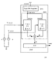
- FIG. 2 is a circuit schematic depicting a VCO with a low frequency tuning gain according to one embodiment.
- a VCO 204 may include a voltage supply such as a high PSR regulator 2041 , a voltage to current converter 2042 and an ICO 2043 .
- the voltage to current converter 2042 may include two voltage to current converters, 2042 A and 2042 B, coupled in parallel between the voltage supply 2041 and the ICO 2043 .
- the converter 2042 A may be controlled by a control voltage V ctrl — A from a voltage source A, which may be, e.g., the output of a loop filter in a PLL.
- the converter 2042 B may be controlled by a control voltage V ctrl — B from a voltage source B, which may be, e.g., a relative DC voltage.
- the converter 2042 A may have a voltage to current converting rate, or trans-conductance, g m — A , and generate a control current I A based on the control voltage V ctrl — A .
- the converter 2042 B may have a trans-conductance g m — B , and generate a control current I B based on the control voltage V ctrl — B .
- Control currents I A and I B may be added at C and a combined control current I C may be provided to the ICO 2043 .
- g m — A :g m — B 1: ⁇ , and ⁇ >1.
- g m — A g m /(1+ ⁇ );
- g m — B ⁇ *g m /( ⁇ +1);
- the trans-conductance g m — A of the converter 2042 A may be only a small part of the trans-conductance g m of the voltage to current converter 2042 .
- V ctrl — B When V ctrl — B is stable, I B may be stable, and l C may only change with V ctrl — A .
- K VCO ′ is the tuning gain from V ctrl — A to the output frequency
- K VCO is the tuning gain from V c to the output frequency
- the tuning gain of the VCO 204 may be reduced to about 1/(1+ ⁇ ) of the tuning gain of the VCO 104 in the known PLL 100 .
- the tuning gain of the VCO 204 may be further decreased. The decrease may only need minimal circuit changes, but may make the VCO 204 significantly less sensitive to the noise from other parts in a PLL.
- FIG. 3 is a circuit schematic depicting a PLL with the VCO in FIG. 2 according to one embodiment.
- a PLL 300 may have a PFD 301 , a charge pump 302 , a loop filter 303 , and a VCO 304 (corresponding to the VCO 204 in FIG. 2 ).
- the charge pump 302 may have a current source 3021 , switches 3022 and 3023 , and a current source 3024 coupled in series between a fixed voltage AVDD and a fixed voltage P.
- Switches 3022 and 3023 may be turned on and off by switching signals PU and PD from the PFD 301 respectively, and may be, e.g., transistors.
- the current sources 3021 and 3024 may provide a current I CP .
- a charge storage device C1 and a resistance device R1 may be coupled in series between the output of the charge pump 302 and the fixed voltage P, and a charge storage device C2 may be coupled between the output of the charge pump 302 and the fixed voltage P as well, in parallel with the circuit branch including the charge storage device C1 and the resistance device R1.
- the charge storage devices C1 and C2 may be, e.g., capacitors, and the resistance device R1 may be, e.g., a resistor.
- a voltage to current converter 3042 A may take its control voltage V ctrl — A from the junction of R1 and C2, and a voltage to current converter 3042 B may take its control voltage V ctrl — B from the junction of R1 and C1.
- the current source 3021 may charge the charge storage device C1 via the switch 3022 and the resistance device R1 to raise the control voltages V ctrl — A and V ctrl — B when the switch 3022 is closed and the switch 3023 is open. Or the charge storage device C1 may discharge via the resistance device R1 and the switch 3023 to lower the control voltages V ctrl — A and V ctrl — B when the switch 3022 is open and the switch 3023 is closed.
- the tuning gain of the VCO 304 may be about 1/(1+ ⁇ ) of that of the known VCO 104 .
- the decrease in tuning gain may make the PLL 300 less sensitive to switching glitches from the charge pump 302 , and the noise from the PFD 301 , the charge pump 302 , and the loop filter 303 .
- FIGS. 4 , 6 and 7 illustrate exemplary circuit implementations of the PLL in FIG. 3 .
- N-type field effect transistors (FETs) MNA and MNB may be used as the voltage to current converters 3042 A and 3042 B in FIG. 3 , and the fixed voltage P may be ground.
- the trans-conductance of MNA is g m — A
- the trans-conductance of MNB is g m — B
- g m — A :g m — B 1: ⁇ , and ⁇ >1
- the gate of MNA may receive the control voltage V ctrl — A
- the gate of MNB may receive the control voltage V ctrl — B
- the drains of MNA and MNB may be coupled to a voltage supply such as a high PSR regulator 4041
- the sources of MNA and MNB may be coupled to an ICO 4043 .
- the control voltage V ctrl — A may control the current I A flowing through MNA
- the control voltage V ctrl — B may control the current I B flowing through MNB.
- a control current l C which is the sum of I A and I B , may control the ICO 4043 .
- MNA and MNB may be native devices, and an output noise of about ⁇ 25 dB PSR from V DD — VCO at the output of the voltage supply to V C at the input of the ICO 4043 may be achieved, as shown in FIG. 5 .
- P-type FETs MPA and MPB may be used as the voltage to current converters 3042 A and 3042 B in FIG. 3 , and the fixed voltage P may be V DD — VCO at the output of a voltage supply such as a high PSR regulator 6041 .
- the trans-conductance of MPA is g m — A
- the trans-conductance of MPB is g m — B
- g m — A :g m — B 1: ⁇ , and ⁇ >1
- the gate of MPA may receive the control voltage V ctrl — A from the junction of C2 and R1
- the gate of MPB may receive the control voltage V ctrl — B from the junction of C1 and R1.
- the source of MPA may be coupled to the voltage supply 6041 via a resistor R a
- the source of MPB may be coupled to the voltage supply 6041 via a resistor R b .
- R b R a / ⁇ .
- the drains of MPA and MPB may be coupled to an ICO 6043 .
- control voltage V ctrl — A may control the current I A flowing through MPA
- control voltage V ctrl — B may control the current I B flowing through MPB
- a control current I C which is the sum of I A and I B , may control the ICO 6043 .
- N-type FETs MNA and MNB may be used as the voltage to current converters 3042 A and 3042 B in FIG. 3 , and the fixed voltage P may be the ground.
- the trans-conductance of MNA is g m — A
- the trans-conductance of MNB is g m — B
- the trans-conductance of MNA is g m — A
- g m_A ⁇ : ⁇ g m_B g m ⁇ + 1 ⁇ : ⁇ g m * ⁇ ⁇ + 1 ⁇ > 1
- the gate of MNA may receive the control voltage V ctrl — A
- the gate of MNB may receive the control voltage V ctrl — B
- the source of MNA may be grounded via a resistor R a
- the source of MNB may be grounded via a resistor R b .
- R b R a / ⁇ .
- the drains of MNA and MNB may be coupled to a voltage supply such as a high PSR regulator 7041 via a current mirror 7044 .
- the current mirror 7044 may have P-type FETs MPP1 and MPP2.
- the junction of the gates of MPP1 and MPP2 and the drain of MPP1 may be coupled to the junction of the drains of MNA and MNB.
- the source of MPP1 may be coupled to the voltage supply 7041 via a resistor R c
- the source of MPP2 may be coupled to the voltage supply 7041 via a resistor R d .
- R d R c /m.
- the drain of MPP2 may be coupled to an ICO 7043 .
- the control voltage V ctrl — A may control the current I A flowing through MNA, and the control voltage V ctrl — B may control the current I B flowing through MNB.
- the reference current of the current mirror 7044 is I C , which is the sum of I A and I B .
- FIG. 8 illustrates a transient simulation result for V ctrl — A and V ctrl — B in FIG. 3 when the PLL 300 is acquiring a lock.
- the control voltage V ctrl — B in the PLL 300 in FIG. 3 may change with the control voltage V ctrl — A slowly, and it may take a few microseconds for V ctrl — B to catch up with the control voltage V ctrl — A .
- the frequency tuning gain of the PLL shown in FIG. 3 may be:
- FIGS. 9A , 9 B, 9 C and 9 D illustrate exemplary relationships between K VCO ′ and the difference between V ctrl — A and V ctrl — B , V ctrl — A ⁇ V ctrl — B , in the PLL 300 of FIG. 3 .
- V ctrl — B is set to a absolutely DC value and the output frequency is scanned by increasing V ctrl — A only
- K VCO ′ may vary significantly with (V ctrl — A ⁇ V ctrl — B ), changing from 220 MHz/V to 450 MHz/V. This may make the bandwidth of the PLL loop vary and deteriorate the loop stability.
- V ctrl — B may be biased with a relative DC voltage, which may follow V ctrl — A in a long period of time.
- V ctrl — B is taken from the junction of R1 and C1. Since C1>>C2, the difference between V ctrl — A , and V ctrl — B may be a DC bias point.
- V ctrl — B is connected to V ctrl — A via R1, V ctrl — B may follow V ctrl — A at last.
- V ctrl_B I CP * ( 1 sC 2 // ( R 1 + 1 sC 1 ) ) ( 12 )
- V ctrl_B I CP * ( 1 sC 2 // ( R 1 + 1 sC 1 ) ) ⁇ 1 sC 1 R 1 + 1 sC 1 ( 13 )
- I A V ctrl — A *g m — A
- I B V ctrl — B *g m — B
- g m_A g m ⁇ + 1
- ⁇ g m_B g m * ⁇ ⁇ + 1 ⁇ :
- H 0 ⁇ ( s ) I CP 2 * ⁇ * ( 1 sC 2 // ( R 1 + 1 sC 1 ) ) * ( 1 ⁇ + 1 + ⁇ ⁇ + 1 * 1 sC 1 R 1 + 1 sC 1 ) * g m * K ICO s * 1 N ( 15 )
- the pole and zero position may be:
- the gain bandwidth may be:
- the output phase noise contributed by R1 at the output frequency ⁇ out of the PLL 300 may be:
- ⁇ n 2 is the output phase noise contributed by R1 at the output frequency ⁇ out of the PLL 100 .
- equation (18) indicates that the pole over zero ratio of the PLL 300 is 1/(1+ ⁇ ) times of that of the known PLL 100 . This will make the PLL loop unstable.
- equation 20 indicates that, due to the frequency tuning gain K VCO is reduced to 1/(1+ ⁇ ) times, the phase noise contribute by R1 is reduced to 1/(1+ ⁇ ) 2 times.
- One way to improve the loop stability of the PLL 300 may be to increase the value of C1 to its (1+ ⁇ ) times. However, this may make the die size consumption unacceptable, since C1 is a big capacitor.
- Another way to improve the loop stability of the PLL 300 may be to decrease the value of C2 to its 1/(1+ ⁇ ) and increase the value of R1 to its (1+ ⁇ ) times. Since the resistor may become R1*(1+ ⁇ ), which will contribute 4*K*T*R1*(1+ ⁇ ) to the noise, the noise reduction benefit depicted by equation 20 may be substituted with equation 23. Equation 23 also indicates that, in the PLL 300 , the phase noise contributed by the filter resistor R1 may be improved to 1/(1+ ⁇ ) times of that in the PLL 100 . Properties of such a PLL may be:
- FIG. 10 is a circuit schematic depicting a PLL corresponding to the PLL 300 of FIG. 3 , with the VCO 304 corresponding to VCO 204 in FIG. 2 , but with a passive loop filter with capacitor multiplication according to one embodiment.
- a replica charge pump 1002 may be added to construct an equivalent capacitor multiplication for C1.
- the replica charge pump 1002 may have a current source 10021 , switches 10022 and 10023 , and a current source 10024 coupled in series between the fixed voltage AVDD and the fixed voltage P, in parallel with the charge pump 302 .
- the switch 10022 may be controlled by the switching signal PD from the PFD 301 , and be turned on and off approximately simultaneously with the switch 3022 , but in the opposite direction.
- the switch 10023 may be controlled by the switching signal PU from the PFD 301 , and be turned on and off approximately simultaneously with the switch 3023 , but in the opposite direction.
- the junction of R1 and C1 in the loop filter 303 from where the control voltage V ctrl — B of the voltage to current converter 3042 B is taken, may be coupled to the junction of switches 10022 and 10023 .
- the current provided by the current source 10021 may be a times the current provided by the current source 3021 in the charge pump 302 , wherein ⁇ 1.
- the PFD 301 may output switching signals PU and PD to the charge pump 302 and the replica charge pump 1002 , closing switches 3022 and 10023 and keeping switches 3023 and 10022 open.
- f ⁇ 1/(C1R1) since 1/(sC2)>>(R1+1/(sC1), most of the current I CP coming from the current source 3021 in the charge pump 302 may go through C1.
- the PFD 301 may send switching signals PU and PD to the charge pump 302 and 1002 , keeping switches 3022 and 10023 open while closing switches 3023 and 10022 . Consequently, C1 may discharge via R1 and the switch 3023 and the discharge current is I CP . At the same time, the current source 10022 may charge C1 via the switch 10022 and R1, and the charging current may be ⁇ *I CP .
- the PFD 301 may keep the switches 3022 and 3023 in the charge pump 302 and switches 10022 and 10023 in the replica charge pump closed to maintain the relationship.
- the frequency tuning gain of the PLL 1000 may be similar to that of PLL 300 . However, since the variation of V ctrl — B is significantly reduced, the loop stability of PLL 1000 may be much better than that of PLL 300 .
- Properties of the PLL 1000 may be:
- V ctrl_A I CP ⁇ ( 1 sC 2 // ( R 1 + 1 sC 1 ) ) - I CP ⁇ ⁇ ⁇ ( 1 sC 1 // ( R 1 + 1 sC 2 ) ) ⁇ 1 sC 2 R 1 + 1 sC 2 ( 24 )
- V ctrl_B I CP ⁇ ( 1 sC 2 // ( R 1 + 1 sC 1 ) ) ⁇ 1 sC 1 R 1 + 1 sC 1 - I CP ⁇ ⁇ ⁇ ( 1 sC 1 // ( R 1 + 1 sC 2 ) ) ( 25 )
- I A V ctrl — A *g m — A
- I B V ctrl — B *g m — B
- the open loop transfer function may be:
- H o ⁇ ( s ) I cp 2 * ⁇ * 1 1 + ⁇ * s * ( R 1 * C 1 - R 1 * C 2 * ⁇ * ⁇ ) + ( 1 + ⁇ ) * ( 1 - ⁇ ) s * ( s * R 1 * C 1 * C 2 + C 1 + C 2 ) * g m * K ICO s * 1 N ( 27 )
- the output phase noise contributed by R1 may be:
- Equation (30) may indicate that the ratio of pole and zero position of the PLL 1000 in FIG. 10 is better than that of PLL 300 in FIG. 3 (expressed by equation (17)), and is similar to that of PLL 100 in FIG. 1 (expressed by equation (3)).
- Equation (31) may indicate that the output phase noise contributed by R1 in the PLL 1000 may be 1/(1+ ⁇ ) times of that in the PLL 300 (expressed by equation (19)), and 1/(1+ ⁇ ) 2 times of that in the PLL 100 .
- PLL 1000 and PLL 300 may reduce the frequency tuning gain to about 1/(1+ ⁇ ) of that of the known PLL 100 .
- PLL 1000 may reduce the output noise contributed by R1 to 1/(1+ ⁇ ) times of that in the PLL 300 , and 1/(1+ ⁇ ) 2 times of that in the PLL 100 .
- the PLL 1000 may achieve similar loop stability of that of PLL 100 without increasing the size of C1, C2 or R1.
- Table 1 is an exemplary performance comparison between a known PLL 100 and a PLL 1000 according to one embodiment.
- BJTs bipolar junction transistors
- JFETs junction gate field-effect transistors
Landscapes
- Stabilization Of Oscillater, Synchronisation, Frequency Synthesizers (AREA)
Abstract
Description
g m =g m
g m
g m
V C =V ctrl
g m
g m
then:
| Conventional Structure | This Work | |||
| Kvco | 1.5 | GHz/V | 0.3 | GHz/V | |
| fo | 1.3 | GHz | 1.3 | GHz | |
| fref | 26 | MHz | 26 | | |
| N | |||||
| 50 | 50 |
| α | No data | 7/8 |
| β | No |
4 |
| |
270 | uA | 340 | | |
| R1 | |||||
| 2 | kΩ | 8 | kΩ | ||
| C1 | 120 | |
30 | | |
| C2 | |||||
| 8 | |
2 | PF | ||
| fc | 2.6 | MHz | 2.6 | MHz | |
| fz | 0.65 | MHz | 0.575 | MHz | |
| fp | 10.35 | MHz | 11.04 | MHz | |
| Phase Margin | 60 | Degree Celsius | 63 | Degree Celsius |
| Phase Noise | −106.3 dBc @ 1.5 MHz | −118 dBc @ 1.5 MHz | |
| contribute by |
| R1 at the out- | |||
| put frequency | |||
Claims (20)
Priority Applications (1)
| Application Number | Priority Date | Filing Date | Title |
|---|---|---|---|
| US12/498,989 US7990225B1 (en) | 2008-07-08 | 2009-07-07 | Low-jitter phase-locked loop |
Applications Claiming Priority (2)
| Application Number | Priority Date | Filing Date | Title |
|---|---|---|---|
| US7896208P | 2008-07-08 | 2008-07-08 | |
| US12/498,989 US7990225B1 (en) | 2008-07-08 | 2009-07-07 | Low-jitter phase-locked loop |
Publications (1)
| Publication Number | Publication Date |
|---|---|
| US7990225B1 true US7990225B1 (en) | 2011-08-02 |
Family
ID=44314364
Family Applications (1)
| Application Number | Title | Priority Date | Filing Date |
|---|---|---|---|
| US12/498,989 Expired - Fee Related US7990225B1 (en) | 2008-07-08 | 2009-07-07 | Low-jitter phase-locked loop |
Country Status (1)
| Country | Link |
|---|---|
| US (1) | US7990225B1 (en) |
Cited By (4)
| Publication number | Priority date | Publication date | Assignee | Title |
|---|---|---|---|---|
| US8362848B2 (en) * | 2011-04-07 | 2013-01-29 | Qualcomm Incorporated | Supply-regulated VCO architecture |
| US8773209B2 (en) * | 2012-08-15 | 2014-07-08 | Phison Electronics Corp. | Frequency generating system, voltage-controlled oscillator module and method for adjusting signal frequency |
| US10396806B1 (en) | 2018-06-05 | 2019-08-27 | M31 Technology Corporation | Voltage regulator based loop filter for loop circuit and loop filtering method |
| EP4091251A4 (en) * | 2020-01-15 | 2023-07-26 | Analog Bits, Inc. | Method and circuits for reducing noise in phase-locked loops |
Citations (4)
| Publication number | Priority date | Publication date | Assignee | Title |
|---|---|---|---|---|
| US5691669A (en) * | 1996-01-11 | 1997-11-25 | Hewlett-Packard Co. | Dual adjust current controlled phase locked loop |
| US20040095188A1 (en) * | 2002-11-06 | 2004-05-20 | Puma Giuseppe Li | Current source circuit for generating a low-noise current and method of operating the current source circuit |
| US20080042759A1 (en) * | 2006-08-21 | 2008-02-21 | Nec Electronics Corporation | PLL circuit |
| US7812650B2 (en) * | 2007-12-21 | 2010-10-12 | Hynix Semiconductor Inc. | Bias voltage generation circuit and clock synchronizing circuit |
-
2009
- 2009-07-07 US US12/498,989 patent/US7990225B1/en not_active Expired - Fee Related
Patent Citations (4)
| Publication number | Priority date | Publication date | Assignee | Title |
|---|---|---|---|---|
| US5691669A (en) * | 1996-01-11 | 1997-11-25 | Hewlett-Packard Co. | Dual adjust current controlled phase locked loop |
| US20040095188A1 (en) * | 2002-11-06 | 2004-05-20 | Puma Giuseppe Li | Current source circuit for generating a low-noise current and method of operating the current source circuit |
| US20080042759A1 (en) * | 2006-08-21 | 2008-02-21 | Nec Electronics Corporation | PLL circuit |
| US7812650B2 (en) * | 2007-12-21 | 2010-10-12 | Hynix Semiconductor Inc. | Bias voltage generation circuit and clock synchronizing circuit |
Non-Patent Citations (7)
| Title |
|---|
| A. Maxim, "Spur and Noise Reduction Techniques in Ring Oscillator Based Frequency Synthesizers for Broadcast Receiver SoCs", Silicon Laboratories Inc., 2008 IEEE, pp. 383-386. |
| A. Maxim, and M. Gheorghe, "A sub-1psrms jitter 1-5GHz 0.13 mum CMOS PLL Using a Passive Feedforward Loop Filter with Noiseless Resistor Multiplication",RMO3B-1, 2005 IEEE Radio Frequency Integrated Circuits Symposium, pp. 207-210. |
| A. Maxim, and M. Gheorghe, "A sub-1psrms jitter 1-5GHz 0.13 μm CMOS PLL Using a Passive Feedforward Loop Filter with Noiseless Resistor Multiplication",RMO3B-1, 2005 IEEE Radio Frequency Integrated Circuits Symposium, pp. 207-210. |
| Ali Hajimiri, Sotirios Limotyrakis and Thomas H. Lee, "Jitter and Phase Noise in Ring Oscillators", IEEE Journal of Solid-State Circuits, vol. 34, No. 6, Jun. 1999, pp. 790-804. |
| Chan-Hong Park, and Beomsup Kim, "A Low-Noise, 900-MHz VCO in 0.6-mum CMOS", IEEE Journal of Solid-State Circuits, vol. 34, No. 5, May 1999, pp. 586-591. |
| Chan-Hong Park, and Beomsup Kim, "A Low-Noise, 900-MHz VCO in 0.6-μm CMOS", IEEE Journal of Solid-State Circuits, vol. 34, No. 5, May 1999, pp. 586-591. |
| Liang Dai and Ramesh Harjani, "Design of Low-Phase-Noise CMOS Ring Oscillators", IEEE Transactions on Circuits and Systems-II: Analog and Digital Signal Processing, vol. 49, No. 5, May 2002, pp. 328-338. |
Cited By (5)
| Publication number | Priority date | Publication date | Assignee | Title |
|---|---|---|---|---|
| US8362848B2 (en) * | 2011-04-07 | 2013-01-29 | Qualcomm Incorporated | Supply-regulated VCO architecture |
| US8773209B2 (en) * | 2012-08-15 | 2014-07-08 | Phison Electronics Corp. | Frequency generating system, voltage-controlled oscillator module and method for adjusting signal frequency |
| US10396806B1 (en) | 2018-06-05 | 2019-08-27 | M31 Technology Corporation | Voltage regulator based loop filter for loop circuit and loop filtering method |
| TWI684329B (en) * | 2018-06-05 | 2020-02-01 | 円星科技股份有限公司 | Voltage regulator based loop filter for loop circuit and loop filtering method |
| EP4091251A4 (en) * | 2020-01-15 | 2023-07-26 | Analog Bits, Inc. | Method and circuits for reducing noise in phase-locked loops |
Similar Documents
| Publication | Publication Date | Title |
|---|---|---|
| US5635879A (en) | Voltage controlled oscillator formed of two differential transconductors | |
| US7233214B2 (en) | Voltage-controlled oscillators with controlled operating range and related bias circuits and methods | |
| US20060141963A1 (en) | Method and apparatus to reduce the jitter in wideband PLL frequency synthesizers using noise attenuation | |
| US7719328B2 (en) | Self-biased phase locked loop | |
| US7176737B2 (en) | Phase-locked loop and delay-locked loop including differential delay cells having differential control inputs | |
| EP1266453B1 (en) | High noise rejection voltage-controlled ring oscillator architecture | |
| US6873214B2 (en) | Use of configurable capacitors to tune a self biased phase locked loop | |
| US20120256693A1 (en) | Supply-regulated vco architecture | |
| US6954090B2 (en) | Charge pump having reduced switching noise | |
| US7145400B2 (en) | Phase locked loop with a switch capacitor resistor in the loop filter | |
| US7327195B2 (en) | PLL frequency synthesizer | |
| US7764092B2 (en) | Phase locked loop and phase locking method | |
| US7688122B2 (en) | Charge pump with cascode biasing | |
| CN108270542A (en) | Frequency band selection clock data recovery circuit and associated method | |
| US10069411B2 (en) | Differential charge pump with extended output control voltage range | |
| US7990225B1 (en) | Low-jitter phase-locked loop | |
| US20080309414A1 (en) | Voltage controlled oscillator and phase locked loop circuit incorporating the same | |
| US7498885B2 (en) | Voltage controlled oscillator with gain compensation | |
| Park et al. | Two-stage feedback-looped charge-pump for spur reduction in CMOS PLL | |
| US7295079B2 (en) | Current-controlled oscillator | |
| US6724273B1 (en) | Filter circuitry for voltage controlled oscillator | |
| US20220038105A1 (en) | Charge pump phase locked loop with low controlled oscillator gain | |
| US20020167366A1 (en) | LC controllable oscillator, a quadrature oscillator and a communication arrangement | |
| US7394329B2 (en) | Analog varactor | |
| US10985767B2 (en) | Phase-locked loop circuitry having low variation transconductance design |
Legal Events
| Date | Code | Title | Description |
|---|---|---|---|
| AS | Assignment |
Owner name: MARVELL SEMICONDUCTOR, INC., CALIFORNIA Free format text: ASSIGNMENT OF ASSIGNORS INTEREST;ASSIGNORS:SONG, YONGHUA;SHUI, TAO;SIGNING DATES FROM 20090624 TO 20090706;REEL/FRAME:022929/0886 |
|
| AS | Assignment |
Owner name: MARVELL INTERNATIONAL LTD., BERMUDA Free format text: ASSIGNMENT OF ASSIGNORS INTEREST;ASSIGNOR:MARVELL SEMICONDUCTOR, INC.;REEL/FRAME:022945/0251 Effective date: 20090708 Owner name: MARVELL TECHNOLOGY (SHANGHAI) LTD., CHINA Free format text: ASSIGNMENT OF ASSIGNORS INTEREST;ASSIGNORS:GUO, JIANMIN;LI, YIHUI;XUE, HONG;AND OTHERS;SIGNING DATES FROM 20090703 TO 20090710;REEL/FRAME:022945/0237 |
|
| AS | Assignment |
Owner name: MARVELL INTERNATIONAL LTD., BERMUDA Free format text: ASSIGNMENT OF ASSIGNORS INTEREST;ASSIGNOR:MARVELL TECHNOLOGY (SHANGHAI) LTD.;REEL/FRAME:025209/0882 Effective date: 20101026 |
|
| STCF | Information on status: patent grant |
Free format text: PATENTED CASE |
|
| FPAY | Fee payment |
Year of fee payment: 4 |
|
| FEPP | Fee payment procedure |
Free format text: MAINTENANCE FEE REMINDER MAILED (ORIGINAL EVENT CODE: REM.); ENTITY STATUS OF PATENT OWNER: LARGE ENTITY |
|
| LAPS | Lapse for failure to pay maintenance fees |
Free format text: PATENT EXPIRED FOR FAILURE TO PAY MAINTENANCE FEES (ORIGINAL EVENT CODE: EXP.); ENTITY STATUS OF PATENT OWNER: LARGE ENTITY |
|
| STCH | Information on status: patent discontinuation |
Free format text: PATENT EXPIRED DUE TO NONPAYMENT OF MAINTENANCE FEES UNDER 37 CFR 1.362 |
|
| FP | Expired due to failure to pay maintenance fee |
Effective date: 20190802 |