US7979814B1 - Model implementation on GPU - Google Patents
Model implementation on GPU Download PDFInfo
- Publication number
- US7979814B1 US7979814B1 US12/047,222 US4722208A US7979814B1 US 7979814 B1 US7979814 B1 US 7979814B1 US 4722208 A US4722208 A US 4722208A US 7979814 B1 US7979814 B1 US 7979814B1
- Authority
- US
- United States
- Prior art keywords
- gpu
- model evaluation
- model
- data
- cpu
- Prior art date
- Legal status (The legal status is an assumption and is not a legal conclusion. Google has not performed a legal analysis and makes no representation as to the accuracy of the status listed.)
- Active, expires
Links
Images


Classifications
-
- G—PHYSICS
- G06—COMPUTING; CALCULATING OR COUNTING
- G06F—ELECTRIC DIGITAL DATA PROCESSING
- G06F30/00—Computer-aided design [CAD]
- G06F30/30—Circuit design
- G06F30/36—Circuit design at the analogue level
- G06F30/367—Design verification, e.g. using simulation, simulation program with integrated circuit emphasis [SPICE], direct methods or relaxation methods
-
- G—PHYSICS
- G06—COMPUTING; CALCULATING OR COUNTING
- G06T—IMAGE DATA PROCESSING OR GENERATION, IN GENERAL
- G06T17/00—Three dimensional [3D] modelling, e.g. data description of 3D objects
-
- G—PHYSICS
- G06—COMPUTING; CALCULATING OR COUNTING
- G06T—IMAGE DATA PROCESSING OR GENERATION, IN GENERAL
- G06T2200/00—Indexing scheme for image data processing or generation, in general
- G06T2200/28—Indexing scheme for image data processing or generation, in general involving image processing hardware
Definitions
- the present invention relates to electronic design automation (EDA) software, and more particularly, to implementing such software in a graphical processing unit.
- EDA electronic design automation
- Integrated circuits continue to advance rapidly and are being widely used in many applications such as computers, consumer electronics, networking, and telecommunications.
- integrated circuits including microprocessors, microcontrollers, application specific integrated circuits (ASICs), gate arrays, programmable logic devices (PLDs), field programmable gate arrays (FPGAs), dynamic random access memories (DRAMs), static random access memories (SRAMs), erasable programmable read only memories (EPROMs), electrically erasable programmable read only memories (EEPROMs), and Flash memories.
- ASICs application specific integrated circuits
- PLDs programmable logic devices
- FPGAs field programmable gate arrays
- DRAMs dynamic random access memories
- SRAMs static random access memories
- EPROMs erasable programmable read only memories
- EEPROMs electrically erasable programmable read only memories
- Design automation tools are needed to simplify and expedite the task of designing an integrated circuit. It is important to be able to accurately predict and estimate the performance of an integrated circuit before the integrated circuit is fabricated. Techniques are needed to provide accurate, fast estimates of the performance of an integrated circuit. It is often desirable in the microelectronics industry to be able to implement physical solutions in as little time as possible for coping with new market opportunities and/or emerging problems. Computer-aided simulations are often used to predict the behaviors of the electrical circuits before they are manufactured. This is done so that design errors are corrected and design parameters are optimized prior to production. It is well known, for example, to use computers and software simulators such as SPICE for obtaining fairly accurate predictions of the analog behaviors of complex circuitry. A number of logic design tools are also commercially available.
- a method in accordance with one embodiment of the present invention, includes a number of steps adapted to perform model evaluation in a graphical processing unit (GPU).
- a multitude of first texture data corresponding to size parameters of devices are stored.
- a multitude of second texture data corresponding to instance parameters of the devices are stored.
- a multitude of third texture data corresponding to models of the devices are stored.
- a multitude of fourth texture data corresponding to terminal voltages received by the device are stored.
- a multitude of links linking each device instance to an associated device model, size parameters and instance parameters are stored.
- a quad having a size defined by the multitude of links is drawn by the quad in the GPU. Each thread in the quad is assigned to a different one of the multitude of links. The computations are carried out in each thread using the linked data to perform the model evaluation.
- the first, second, third and fourth multitude of texture data are received from a CPU.
- the GPU stamps its output data by converting the output data of the GPU from a device instance based format to a matrix pointer based format.
- the GPU output data has a format defined by device instances. IN one embodiment, the stamped data are transferred to the CPU.
- model evaluation is divided into a multitude of model evaluation parts to avoid GPU shader length limit. Each model evaluation part is assigned to a different GPU kernel.
- model evaluation parts include, in part, current-voltage model evaluation part, capacitance-voltage model evaluation part, and junction evaluation part.
- a system adapted to perform model evaluation during a design or verification of an integrated circuit includes, in part, a central processing unit (CPU) and a graphical processing unit (GPU).
- the CPU is adapted to (i) store a multitude of first texture data corresponding to device size parameters; (ii) store a multitude of second texture data corresponding to device instance parameters; (iii) store a multitude of third texture data corresponding to models of the devices; (iv) store a multitude of fourth texture data corresponding to terminal voltages received by the devices; and (v) store a multitude of links linking each device instance to an associated device model, size parameters and instance parameters.
- the GPU is adapted to (i) draw a quad having a size defined by the number of the multitude of links; (ii) assign each thread in the quad to a different one of the multitude of links; and (iii) to carry out computations in each thread using the linked data to perform the model evaluation.
- the GPU is further adapted to stamp its output data by convert its output data from a device instance based format to a matrix pointer based format.
- the GPU output data has a format defined by the device instances.
- the GPU is further adapted to perform double precision emulation to achieve double precision floating point accuracy.
- a control logic is adapted to switch model evaluation operation between the GPU and the CPU to achieve double precision floating point accuracy.
- the GPU is further adapted to divide the model evaluation operation into a multitude of model evaluation parts so as to avoid GPU shader length limit and to assign each model evaluation part to a different one of the GPU kernels.
- the multitude of model evaluation parts includes current-voltage model evaluation part, capacitance-voltage model evaluation part, and junction evaluation part.
- FIG. 1 shows model evaluation data that is organized as a linked list for use by a CPU, as known in the prior art.
- FIGS. 2A-2G show various 2D texture data structure for use by a GPU to perform model evaluation/simulation/verification, in accordance with one embodiment of the present invention.
- FIGS. 3A-3C show the format of the data used by the GPU before and after the stamping process, in accordance with one embodiment of the present invention.
- FIGS. 4A-4C show the data structure of the pointer to model output map as used by the GPU, in accordance with one embodiment of the present invention.
- FIG. 5 is a flowchart of steps carried to perform model evaluation, circuit simulation and/or design verification, in accordance with one exemplary embodiment.
- FIG. 6 is a flowchart of steps performed by the CPU and the GPU for a time step during model evaluation, circuit simulation and/or design verification, in accordance with one exemplary embodiment.
- FIG. 7 is a flowchart of steps performed by the GPU for each time step, in accordance with one exemplary embodiment. of the present invention.
- FIG. 8 is a flowchart of steps performed by the GPU during model evaluation, in accordance with one exemplary embodiment of the present invention.
- FIG. 9 is a flowchart of steps performed by the GPU to stamp data, in accordance with one exemplary embodiment of the present invention.
- FIG. 10 is a block diagram of a computer system adapted to perform model evaluation, in accordance with one exemplary embodiment of the present invention.
- model evaluations and simulations associated with design of integrated circuits are carried out by a graphical processing unit (GPU).
- the GPU is used as an independent model engine controlled by a central processing unit (CPU).
- CPU central processing unit
- model evaluations are treated as a part of the GPU simulation flow. Accordingly, in these embodiments, the model evaluation results are not transferred back to the CPU. Below are the steps performed in accordance with such embodiments:
- the steps performed by the second exemplary embodiment are a subset of those performed by the first exemplary embodiment. Accordingly, the following is a description of the GPU model evaluation of the first exemplary embodiment.
- model evaluation In CPU, data used in model evaluation are usually organized as a linked list for model, instance data structures, sizes, etc., as shown in FIG. 1 .
- Bsim 3 , Bsim 4 are different device models for MOSFET transistors
- BJT is a device model for bipolar transistors.
- Each model includes a set of equations that describe the electrical characteristics of that transistor using a particular set of model parameters values (model card).
- each of those models point to a link list of model cards.
- a model card is a group of model parameter used to define a model behavior.
- Each model card applies to one or more instances of a component.
- model card Models 1 is shown as being applicable to instances inst 1 , inst 2 , inst 3 , etc. of a component.
- Each instance in FIG. 1 may be a MOSFET component used in the circuit being simulated for design.
- instances inst 1 and inst 2 have same feature sizes (such as channel length and channel width), and thus share a subset of parameters, stored in size parameter structure, Size 1 of FIG. 1 .
- the size structure is used to save memory, since multiple instance share one size structure.
- Instance inst 3 is shown as having a feature size Size 2 .
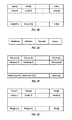
- FIGS. 2A-2G show the link list structure of FIG. 1 .
- FIGS. 2A-2D show the data that is received and used by the GPU.
- FIG. 2A shows the 2D texture model data used in a GPU.
- FIG. 2B shows the 2D texture instance parameter values used in the GPU.
- FIG. 2C shows the 2D texture size parameter values used in the GPU.
- Each block of data in FIG. 2A represents a model. For example, Model[ 1 ] of FIG. 2A is associated with model card Model 1 of FIG. 1 , and Model[ 2 ] of FIG. 2A is associated with model card Model 2 of FIG. 1 .
- each entry in FIG. 2D represents a link associating an instance to the models and parameter sizes used for that instance.
- Each link entry such as Link[ 1 ] includes 3 integer, namely a model index, an instance index, and a size index.
- FIG. 2E shows the indices associated with each link entry of FIG. 2D .
- Each index in FIG. 2E points to a starting point in either a model, an instance, or a parameter size. Using these indices as the starting point and the link entry in FIG. 2D , the GPU receives the texture locations where the model parameters, instance parameters and size parameters are stored, thus enabling the GPU to start model evaluation.
- Float 4 data type is used to store the data.
- each entry in FIG. 2E is a Float 4 data type, including 4 floating point numbers: namely the model index, instance index, size parameter index, and a dummy
- Each link entry is assigned to a thread in the GPU. From the thread coordinates, the link entry can be accessed from the texture data containing the information of the link entries.
- Each entry in FIG. 2D includes 3 numbers that are shown in FIG. 2E , and that are used by associated the thread to access further parameters.
- One of the 3 numbers is shown as ModelIndex, which the GPU thread uses to locate the position of the model used for this instance from FIG. 2A .
- the second of the 3 numbers in FIG. 2E is InstIndex, and that is used by the GPU thread to locate the position of the instance parameters from FIG. 2B .
- the third of the 3 numbers in FIG. 2E is SizeIndex, which is used to locate the size parameters of the instance from FIG. 2C . Thereafter, another 3 texture data are accessed based on the index information, to get the model data, instance data and parameter size data for that instance. These data are then used by the kernel of GPU for model evaluation.
- the pixels associated with the coordinates of the quad drawn by the GPU are supplied by the CPU to the GPU.
- FIG. 2G shows pixel coordinates of such a quad. These pixels have a one-to-one relation to the links shown in FIG. 2D .
- the pixel coordinates ate thus used to locate the associated links entries, as shown in FIG. 2D .
- the GPU assigns a thread to each pixel.
- the terminal voltages for each instance are required.
- Model parameters, instance parameters and size parameters are all static, i.e., their values are not changed during simulation.
- the solution vector (the vector containing the terminal voltages for each instance) changes during the simulation.
- Solution vector is calculated from engine/solver based on model evaluation results.
- the CPU packs the updated solution vector into the format shown in FIG. 2F and transfers the packed data to into GPU.
- the instance data stored in FIG. 2B includes the terminal indices which are the indices to the solution vector. The indices are used by the GPU to retrieve the terminal voltages for that instance.
- the GPU retrieves the terminal indices. From the terminal indices and the solution vector, the GPU retrieves the terminal voltages for each instance.
- model outputs are packed by the GPU in manner similar to that shown in the data structure of FIG. 2B .
- the model evaluation is divided into a number of parts, where each kernel is assigned to one such part.
- the model evaluation is divided into 3 parts, namely a current-voltage model evaluation part, capacitance-voltage model evaluation part, and junction evaluation part.
- FIGS. 3A and 3B show the data format before and after the stamping process, respectively. Because the data size after the stamping process is typically smaller than that before the stamping, the data size to be transferred to CPU from GPU is reduced, thereby increasing the performance of data transfer.
- FIG. 3A shows an exemplary data structure associated with the output of the model evaluation based on the instance data and before the stamping. This data has the same structure as the link entries shown in FIG. 2D .
- FIG. 3B shows the data structure of matrix pointers obtained from FIG. 3A after the stamping. Data in FIG. 3B are organized according to matrix pointer sequence of the matrix to be solved by simulator solver. Each entry in the data shown in FIG. 3B corresponds to one pointer of the matrix in the simulator. To effectuate the stamping, each data in FIG. 3A is added to a position in FIG. 3B . Because, in accordance with the stamping technique, multiple data associated with the structure in FIG. 3A are added together into a single entry associated with the structure in FIG. 3B , the size of the data after the stamping is often smaller than the size of the data before the stamping operation is performed.
- a pointer to model output map is setup before the model evaluation and transfer of the data from the CPU to GPU.
- a map is used herein to refer to a link between two sets of data.
- Each model output shown in FIG. 3A is linked with (i.e., mapped to) one entry in FIG. 3B . It may also be possible that multiple data in FIG. 3A are linked to one location in FIG. 3B .
- the static data structure of the pointer to model output is not changed during simulation if the matrix structure is not changed.
- the data structure of the pointer to model output map is shown in FIGS. 4A through 4C .
- the matrix structure is often not changed during simulation. However, In a rare case, if during the simulation, the matrix structure is changed, then the data structure of the pointer to model output map is rebuilt to account for this change.
- a quad is drawn that has the same size as the number of entries shown in FIG. 4B , i.e., the number of matrix pointer to be stamped.
- Each matrix pointer is assigned to a thread.
- Each group of entries in FIG. 4A points to a location in FIG. 3A associated with a matrix pointer in FIG. 3B .
- entries O 1 ForP 1 through O 1 ForP 1 collectively define an index in FIG. 3A that are added together to collectively define the location for matrix pointer Pointer[ 1 ] of FIG. 3B .
- the pixels associated with the coordinates of the quad drawn by the GPU for stamping are supplied by the CPU to the GPU.
- FIG. 3C shows pixel coordinates of such a quad.
- These pixels have a one-to-one relation to the indices shown in FIG. 4B and with the same coordinates.
- the GPU assigns a thread to each pixel.
- the pixel coordinates are then used to locate the associated entries shown in FIG. 4B .
- the entries in FIG. 4B are subsequently used to locate the entries in FIGS. 4A and 4C .
- Each entry in FIG. 4B is used as an index to define a pointer in FIG. 3B .
- the table shown in FIG. 4B thus has the same size as the table shown in FIG. 3B .
- the value of each entry in FIG. 4B is the starting point (the index) of a data entry in FIG. 4A for the associated matrix pointer in FIG. 3B .
- the number of entries in FIG. 4C is the same as the number of entries in FIG. 4B .
- Each entry in FIG. 4C represents the total data number of entries needed from a corresponding entry in FIG. 3A and that are to be added together to define a corresponding location in FIG. 3B .
- Index[ 2 ] in FIG. 4B defines the location of O 1 ForP 2 in FIG.
- GPU can locate the first map information for pointer 2 .
- Num[ 2 ] in FIG. 4C and determine how many output to pointer map entries are there for pointer 2 .
- the GPU will then access total Num[ 2 ] entries in FIG. 4A to collect all the output to pointer map entries for pointer 2 .
- GPU can locate the model evaluation output from FIG. 3A .
- Such a map entry is actually an index to one data stored in data shown in FIG. 3A . Accordingly, the entries in FIG. 4B and FIG. 4C have a one-to-one mapping relationship.
- the GPU uses the coordinates corresponding to each thread to locate and associate the various entries in FIGS. 4B and 4C . Using these entries, the GPU identifies the starting index and number of data for each matrix pointer. The index and number of data are thereafter used to locate the entries in FIG. 3A . The required entries in FIG. 3B are subsequently added to one another to define a corresponding location in FIG. 3B .
- the data stamped in the GPU is thereafter transferred from the GPU to the CPU.
- the data received by the CPU is subsequently stamped into a matrix for further processing by the CPU.
- GPUs can only provide single precision floating point accuracy, which may not be good enough for circuit simulation.
- two techniques to this problem are provided.
- double precision emulation in GPU is carried out.
- a structure containing two single precision floating pointer numbers is generated to emulate a double precision floating point number.
- one floating point number contains the major digits of the double precision number
- the other floating point number contains the minor digits of the double precision number.
- Different techniques may then be used to accomplish double precision accuracy using this data structure for operations, such as addition, subtraction, multiplication and square root operations.
- Minor part of the output is obtained by subtracting the major part of a larger input from the major part of the output
- a CPU model with double precision accuracy determines when and when not to call GPU model evaluation based on the iteration information provided in engine during each Newton step. In the first few iterations, the GPU model is called to evaluation and improve performance. Then after a certain number of iterations, a switch is made to CPU double precision model evaluation routine to improve accuracy.
- FIG. 5 is a flowchart 500 of steps carried to perform model evaluation, circuit simulation and/or design verification, in accordance with one exemplary embodiment.
- a CPU prepares model data, instance data, size data as well as link data in a format suitable by a GPU and transfers this data to the GPU.
- step 510 the activities of the CPU and GPU coordinated and combined to carry out the simulation. Simulation ends in step 530 .
- FIG. 6 is a flowchart 600 of steps performed by the CPU and the GPU for a time step during model evaluation, circuit simulation and/or design verification, in accordance with one exemplary embodiment.
- a new time step is started with an initial solution vector from a DC or an estimate based on the last time point; the iteration number is also set to zero.
- the evaluation/simulation/verification flow (hereinafter flow) is passed 670 to the CPU which continue to advance the flow. If the time step is detected as converging in steps 640 and 650 , the time step simulation is completed 660 .
- step 650 If the time step is detected as not converging in step 650 , the flow returns to step 620 . If at step 620 it is determined that the iteration number is smaller than a predefined value, the flow of the evaluation/simulation/verification is passed 620 to GPU 630 . Thereafter, the GPU continues to compute and proceed with the flow of the evaluation/simulation/verification, at which the process moves to step 640 , as shown in flowchart 600 and shown in FIG. 6 .
- FIG. 7 is a flowchart 700 of steps performed by the GPU for each time step.
- the CPU packs the solution vector and transfers it to the GPU.
- the GPU performs the model evaluation.
- the GPU performs stamping.
- the GPU transfers the stamped data back to the CPU.
- an engine/solver solves the next solution vector based on the model evaluation and stamping results.
- FIG. 8 is a flowchart 800 of steps performed by the GPU during model evaluation.
- the CPU issue an instruction to the GPU to draw a quad having a specified size.
- the GPU assigns a thread to each pixel in the drawn quad, and retrieves the coordinates of the pixels.
- the GPU locates the link data using the pixel coordinates of the pixel.
- the GPU to locate the model parameters, instance parameters and size parameters using the located link information.
- GPU locates the terminal voltages from the solution vector using the terminal indices obtained from the instance parameters.
- the GPU performs current-voltage evaluation using the available data and stores the result of its computations.
- the GPU performs capacitance-voltage evaluation using the available data, and stores the result of its computations.
- the GPU performs junction-voltage evaluations using the available data and store the results.
- FIG. 9 is a flowchart 900 of steps performed by the GPU to stamp data.
- the CPU issues an instruction to the GPU to draw a quad having a specified size.
- the GPU assigns a thread to each pixel in the drawn quad, shown in FIG. 2G 3 C and retrieves the coordinates of the pixels.
- the GPU locates the link data, the number of related stored using the pixel coordinates.
- the GPU locates the model evaluation output index using the results of the operation of step 930 .
- the GPU adds the entries obtained in step 940 for each thread (pixel) together and stored the results of this operation.
- FIG. 10 is a block diagram of a computer system 1000 adapted to perform model evaluation, in accordance with one embodiment of the present invention.
- Computer system 1000 is shown as including a GPU 1010 , a CPU 1020 , a memory 1030 , and a logic block 1030 .
- Memory 1040 stores data used by GPU 1010 and CPU 1020 .
- Logic block 1030 performs logic operations as required by GPU 1010 and CPU 1020
Landscapes
- Engineering & Computer Science (AREA)
- Physics & Mathematics (AREA)
- Computer Hardware Design (AREA)
- Theoretical Computer Science (AREA)
- Geometry (AREA)
- General Physics & Mathematics (AREA)
- Computer Graphics (AREA)
- Software Systems (AREA)
- Microelectronics & Electronic Packaging (AREA)
- Evolutionary Computation (AREA)
- General Engineering & Computer Science (AREA)
- Management, Administration, Business Operations System, And Electronic Commerce (AREA)
Abstract
Description
Claims (17)
Priority Applications (1)
| Application Number | Priority Date | Filing Date | Title |
|---|---|---|---|
| US12/047,222 US7979814B1 (en) | 2007-03-12 | 2008-03-12 | Model implementation on GPU |
Applications Claiming Priority (3)
| Application Number | Priority Date | Filing Date | Title |
|---|---|---|---|
| US89428107P | 2007-03-12 | 2007-03-12 | |
| US97795807P | 2007-10-05 | 2007-10-05 | |
| US12/047,222 US7979814B1 (en) | 2007-03-12 | 2008-03-12 | Model implementation on GPU |
Publications (1)
| Publication Number | Publication Date |
|---|---|
| US7979814B1 true US7979814B1 (en) | 2011-07-12 |
Family
ID=44245662
Family Applications (1)
| Application Number | Title | Priority Date | Filing Date |
|---|---|---|---|
| US12/047,222 Active 2028-08-24 US7979814B1 (en) | 2007-03-12 | 2008-03-12 | Model implementation on GPU |
Country Status (1)
| Country | Link |
|---|---|
| US (1) | US7979814B1 (en) |
Cited By (3)
| Publication number | Priority date | Publication date | Assignee | Title |
|---|---|---|---|---|
| US20130039601A1 (en) * | 2007-06-08 | 2013-02-14 | Apple Inc. | Method and Apparatus for Managing Image-Processing Operations |
| RU2604985C2 (en) * | 2014-11-11 | 2016-12-20 | Федеральное государственное бюджетное образовательное учреждение высшего образования "Воронежский государственный технический университет" (ФГБОУ ВО "ВГТУ", ВГТУ) | Method of calculations on graphics processing units for simulating noise-immunity of low-density codecs |
| CN108280799A (en) * | 2017-01-06 | 2018-07-13 | 中航华东光电(上海)有限公司 | A kind of graphic generator and image generation method based on FPGA |
Citations (10)
| Publication number | Priority date | Publication date | Assignee | Title |
|---|---|---|---|---|
| US20030105620A1 (en) * | 2001-01-29 | 2003-06-05 | Matt Bowen | System, method and article of manufacture for interface constructs in a programming language capable of programming hardware architetures |
| US20040061700A1 (en) * | 2002-09-30 | 2004-04-01 | Hiroyuki Shioya | Image processing apparatus and method of same |
| US20050212811A1 (en) * | 2004-03-24 | 2005-09-29 | Fujitsu Limited | Three-dimensional drawing model generation method, three-dimensional model drawing method, and program thereof |
| US20060087516A1 (en) * | 2000-11-30 | 2006-04-27 | Microsoft Corporation | System, Method, and Computer Program Product for General Environment Mapping |
| US20070195085A1 (en) * | 2005-01-27 | 2007-08-23 | Silicon Graphics, Inc. | System and method for graphics culling |
| US20080235316A1 (en) * | 2007-03-23 | 2008-09-25 | Yun Du | Processor with adaptive multi-shader |
| US7489318B1 (en) * | 2004-05-20 | 2009-02-10 | Nvidia Corporation | Apparatus and method for managing memory to generate a texture from a render target when forming graphical images |
| US7594095B1 (en) * | 2005-11-29 | 2009-09-22 | Nvidia Corporation | Multithreaded SIMD parallel processor with launching of groups of threads |
| US20100118043A1 (en) * | 2006-11-03 | 2010-05-13 | Nvidia Corporation | Reconfigurable high-performance texture pipeline with advanced filtering |
| US20100138376A1 (en) * | 2007-01-24 | 2010-06-03 | Nicholas John Avis | Method and system for searching for patterns in data |
-
2008
- 2008-03-12 US US12/047,222 patent/US7979814B1/en active Active
Patent Citations (10)
| Publication number | Priority date | Publication date | Assignee | Title |
|---|---|---|---|---|
| US20060087516A1 (en) * | 2000-11-30 | 2006-04-27 | Microsoft Corporation | System, Method, and Computer Program Product for General Environment Mapping |
| US20030105620A1 (en) * | 2001-01-29 | 2003-06-05 | Matt Bowen | System, method and article of manufacture for interface constructs in a programming language capable of programming hardware architetures |
| US20040061700A1 (en) * | 2002-09-30 | 2004-04-01 | Hiroyuki Shioya | Image processing apparatus and method of same |
| US20050212811A1 (en) * | 2004-03-24 | 2005-09-29 | Fujitsu Limited | Three-dimensional drawing model generation method, three-dimensional model drawing method, and program thereof |
| US7489318B1 (en) * | 2004-05-20 | 2009-02-10 | Nvidia Corporation | Apparatus and method for managing memory to generate a texture from a render target when forming graphical images |
| US20070195085A1 (en) * | 2005-01-27 | 2007-08-23 | Silicon Graphics, Inc. | System and method for graphics culling |
| US7594095B1 (en) * | 2005-11-29 | 2009-09-22 | Nvidia Corporation | Multithreaded SIMD parallel processor with launching of groups of threads |
| US20100118043A1 (en) * | 2006-11-03 | 2010-05-13 | Nvidia Corporation | Reconfigurable high-performance texture pipeline with advanced filtering |
| US20100138376A1 (en) * | 2007-01-24 | 2010-06-03 | Nicholas John Avis | Method and system for searching for patterns in data |
| US20080235316A1 (en) * | 2007-03-23 | 2008-09-25 | Yun Du | Processor with adaptive multi-shader |
Cited By (4)
| Publication number | Priority date | Publication date | Assignee | Title |
|---|---|---|---|---|
| US20130039601A1 (en) * | 2007-06-08 | 2013-02-14 | Apple Inc. | Method and Apparatus for Managing Image-Processing Operations |
| US8670634B2 (en) * | 2007-06-08 | 2014-03-11 | Apple Inc. | Method and apparatus for managing image-processing operations |
| RU2604985C2 (en) * | 2014-11-11 | 2016-12-20 | Федеральное государственное бюджетное образовательное учреждение высшего образования "Воронежский государственный технический университет" (ФГБОУ ВО "ВГТУ", ВГТУ) | Method of calculations on graphics processing units for simulating noise-immunity of low-density codecs |
| CN108280799A (en) * | 2017-01-06 | 2018-07-13 | 中航华东光电(上海)有限公司 | A kind of graphic generator and image generation method based on FPGA |
Similar Documents
| Publication | Publication Date | Title |
|---|---|---|
| US8117576B2 (en) | Method for using an equivalence checker to reduce verification effort in a system having analog blocks | |
| US6631502B2 (en) | Method of analyzing integrated circuit power distribution in chips containing voltage islands | |
| US7016794B2 (en) | Floor plan development electromigration and voltage drop analysis tool | |
| US6675139B1 (en) | Floor plan-based power bus analysis and design tool for integrated circuits | |
| CN105138774B (en) | A kind of sequential post-simulation method based on the design of integrated circuit levelization | |
| CN104657537B (en) | Design is based on fin formula field effect transistor(FINFET)Circuit method and its implement system | |
| US11301608B2 (en) | Layout-based side-channel emission analysis | |
| CN111488717A (en) | Method, device and equipment for extracting standard unit time sequence model and storage medium | |
| US20170091371A1 (en) | Method of parameter extraction and system thereof | |
| CN101689216B (en) | Compact circuit-simulation output | |
| US20170046470A1 (en) | Process design kit for efficient and accurate mismatch simulation of analog circuits | |
| CN114185895A (en) | Data import and export method and device, electronic equipment and storage medium | |
| US7979814B1 (en) | Model implementation on GPU | |
| JP5173147B2 (en) | System and method for providing concise mapping between different memory systems | |
| US9582626B1 (en) | Using waveform propagation for accurate delay calculation | |
| JP2006190149A (en) | Low power consumption design method for semiconductor integrated circuit | |
| CN116069726B (en) | Management method, equipment and medium of integrated circuit design library | |
| CN103440391A (en) | Semiconductor process corner scanning and simulating method based on numerical value selection function | |
| CN109696614B (en) | Circuit test optimization method and device | |
| US11520960B1 (en) | Register transfer level based side channel leakage assessment | |
| CN101794328B (en) | Fast and accurate estimation of gate output loading | |
| CN103135964B (en) | Across method and the electronic equipment of instruction set call function | |
| US11328109B2 (en) | Refining multi-bit flip flops mapping without explicit de-banking and re-banking | |
| CN109544661B (en) | Area map drawing method, apparatus, computer device and storage medium | |
| CN106528946A (en) | Method for inserting AutoCAD graph blocks in batches |
Legal Events
| Date | Code | Title | Description |
|---|---|---|---|
| AS | Assignment |
Owner name: REVOSYS, INC., CALIFORNIA Free format text: ASSIGNMENT OF ASSIGNORS INTEREST;ASSIGNORS:MA, YUTAO;XU, YI;REEL/FRAME:021187/0435 Effective date: 20080623 |
|
| STCF | Information on status: patent grant |
Free format text: PATENTED CASE |
|
| AS | Assignment |
Owner name: JINAN PROPLUS ELECTRONICS CO., LTD., CHINA Free format text: ASSIGNMENT OF ASSIGNORS INTEREST;ASSIGNOR:REVOSYS, INC;REEL/FRAME:027286/0750 Effective date: 20111121 |
|
| REMI | Maintenance fee reminder mailed | ||
| FPAY | Fee payment |
Year of fee payment: 4 |
|
| SULP | Surcharge for late payment | ||
| AS | Assignment |
Owner name: PROPLUS DESIGN SOLUTIONS, INC., CALIFORNIA Free format text: ASSIGNMENT OF ASSIGNORS INTEREST;ASSIGNOR:JINAN PROPLUS ELECTRONICS CO., LTD.;REEL/FRAME:036686/0111 Effective date: 20150929 |
|
| MAFP | Maintenance fee payment |
Free format text: PAYMENT OF MAINTENANCE FEE, 8TH YR, SMALL ENTITY (ORIGINAL EVENT CODE: M2552); ENTITY STATUS OF PATENT OWNER: SMALL ENTITY Year of fee payment: 8 |
|
| AS | Assignment |
Owner name: JINAN PROPLUS ELECTRONICS CO., LTD., CHINA Free format text: ASSIGNMENT OF ASSIGNORS INTEREST;ASSIGNOR:PROPLUS DESIGN SOLUTIONS, INC.;REEL/FRAME:049338/0620 Effective date: 20190529 |
|
| AS | Assignment |
Owner name: PRIMARIUS TECHNOLOGIES CO., LTD., CHINA Free format text: CHANGE OF NAME;ASSIGNOR:JINAN PROPLUS ELECTRONICS CO., LTD.;REEL/FRAME:054612/0347 Effective date: 20201112 |
|
| MAFP | Maintenance fee payment |
Free format text: PAYMENT OF MAINTENANCE FEE, 12TH YR, SMALL ENTITY (ORIGINAL EVENT CODE: M2553); ENTITY STATUS OF PATENT OWNER: SMALL ENTITY Year of fee payment: 12 |