US7973592B2 - Charge pump with current based regulation - Google Patents
Charge pump with current based regulation Download PDFInfo
- Publication number
- US7973592B2 US7973592B2 US12/506,998 US50699809A US7973592B2 US 7973592 B2 US7973592 B2 US 7973592B2 US 50699809 A US50699809 A US 50699809A US 7973592 B2 US7973592 B2 US 7973592B2
- Authority
- US
- United States
- Prior art keywords
- charge pump
- pump system
- pump circuit
- control signal
- output
- Prior art date
- Legal status (The legal status is an assumption and is not a legal conclusion. Google has not performed a legal analysis and makes no representation as to the accuracy of the status listed.)
- Expired - Fee Related
Links
Images


Classifications
-
- H—ELECTRICITY
- H02—GENERATION; CONVERSION OR DISTRIBUTION OF ELECTRIC POWER
- H02M—APPARATUS FOR CONVERSION BETWEEN AC AND AC, BETWEEN AC AND DC, OR BETWEEN DC AND DC, AND FOR USE WITH MAINS OR SIMILAR POWER SUPPLY SYSTEMS; CONVERSION OF DC OR AC INPUT POWER INTO SURGE OUTPUT POWER; CONTROL OR REGULATION THEREOF
- H02M3/00—Conversion of dc power input into dc power output
- H02M3/02—Conversion of dc power input into dc power output without intermediate conversion into ac
- H02M3/04—Conversion of dc power input into dc power output without intermediate conversion into ac by static converters
- H02M3/06—Conversion of dc power input into dc power output without intermediate conversion into ac by static converters using resistors or capacitors, e.g. potential divider
- H02M3/07—Conversion of dc power input into dc power output without intermediate conversion into ac by static converters using resistors or capacitors, e.g. potential divider using capacitors charged and discharged alternately by semiconductor devices with control electrode, e.g. charge pumps
- H02M3/073—Charge pumps of the Schenkel-type
Definitions
- This invention pertains generally to the field of charge pumps and more particularly to techniques for regulating charge pumps.
- Charge pumps use a switching process to provide a DC output voltage larger or lower than its DC input voltage.
- a charge pump will have a capacitor coupled to switches between an input and an output.
- the charging half cycle the capacitor couples in parallel to the input so as to charge up to the input voltage.
- the transfer half cycle the charged capacitor couples in series with the input voltage so as to provide an output voltage twice the level of the input voltage.
- FIGS. 1 a and 1 b This process is illustrated in FIGS. 1 a and 1 b .
- the capacitor 5 is arranged in parallel with the input voltage V IN to illustrate the charging half cycle.
- the charged capacitor S is arranged in series with the input voltage to illustrate the transfer half cycle.
- the positive terminal of the charged capacitor 5 will thus be 2*V IN with respect to ground.
- Charge pumps are used in many contexts. For example, they are used as peripheral circuits on flash and other non-volatile memories to generate many of the needed operating voltages, such as programming or erase voltages, from a lower power supply voltage.
- a number of charge pump designs, such as conventional Dickson-type pumps, are know in the art. But given the common reliance upon charge pumps, there is an on going need for improvements in pump design, particularly with respect to trying to save on current consumption and reduce the amount ripple in the output of the pump.
- the charge pump system includes a charge pump circuit, connected to receive an input voltage and generate from it an output having a voltage level, and regulation circuitry connected to the charge pump circuit.
- the regulation circuitry includes a voltage comparison section connected to receive the output and a reference voltage and derive from the voltage level the output and the reference voltage a first control signal and a current determination section connected to the charge pump circuit to indirectly determine the amount of current flowing through the charge pump circuit and determine a second control signal based upon the determined amount of current.
- the regulation circuitry also includes a pump control section connected to receive the first and second control signals and derive from them a third control signal, where the charge pump system adapts the operation of the charge pump circuit in response to the third control signal.
- FIG. 1 a is a simplified circuit diagram of the charging half cycle in a generic charge pump
- FIG. 1 b is a simplified circuit diagram of the transfer half cycle in a generic charge pump
- FIG. 2 is a top-level block diagram for a regulated charge pump
- FIGS. 3 and 4 illustrate resistive divider feedback regulation and corresponding regulation of a charge pump system
- FIG. 5 is a top level diagram for a regulated charge pump system using current sensing based regulation
- FIG. 6 shows an implementation of current sensing based regulation
- FIGS. 7-9 illustrate the usage of current sensing based regulation.
- the techniques presented here are widely applicable to various charge pump designs to reduce overall current consumption for charge pump and for output voltage ripple reduction.
- this is done by using a current based regulation method in addition to the typical voltage based regulation methods, where the current flow in the charge pump is determined independently of the output voltage.
- the strength of charge pump can be dynamically adjusted in term of regulation level, branch assignment, clock frequency, clock amplitude, and so on. Relying only on the regulation on output voltage may not achieve best power consumption or ripple reduction since this would only look at the voltage plus noise of voltage.
- Indirectly sensing the current going through pump (not in serial with output stage to allow additional IR drop) will allow the pumps to have matrix of V and I to better adjust the charge pump parameters for current saving and ripple reduction.
- FIG. 2 is a top-level block diagram of a typical charge pump using an output voltage based regulation scheme.
- the pump 201 has as inputs a clock signal and a voltage Vreg and provides an output Vout.
- the clock generation circuit is not explicitly shown in FIG. 2 , although it may be considered part of the charge pump system in some embodiments or taken as an external input.
- the high (Vdd) and low (ground) connections are also not explicitly shown.
- the voltage Vreg is provided by the regulator 203 , which has as inputs a reference voltage Vref from an external voltage source and the output voltage Vout.
- the regulator block 203 generates feedback control signal Vreg such that the desired value of Vout can be obtained.
- the pump section 201 may have any of various designs for charge pumps, such as described in the various references cited above including charge doubler-type circuits with cross-coupled elements as well as the Dickson-type pumps described below for the exemplary embodiments.
- a charge pump is typically taken to refer to both the pump portion 201 and the regulator 203 , when a regulator is included, although in some usages “charge pump” refers to just the pump section 201 .
- the terminology “charge pump system” will often be used to describe pump itself as well as any
- FIG. 3 illustrates an example of using a resistive divider feedback regulation method to generate a regulation control signal.
- FIG. 4A is a schematic view of the pump and some regulation control circuitry that is similar to FIG. 3 , but showing a particular embodiment of a pump.
- R 1 411 , R 2 413 , and Amp 415 can be taken as the similar elements of FIG. 3 .
- the charge pump is shown as a Dickson-type pump of a single branch and four stages.
- the 5 diodes ( 403 - 0 , 403 - 1 , 403 - 2 , 403 - 3 , 403 - 4 ) are formed of diode connected transistors connected in series between the input at voltage Vcc and the output node.
- a capacitor ( 405 - 1 , 405 - 2 , 405 - 3 , 405 - 2 ) has one plate connected, the other plate connected to one of a pair of non-overlapping clock signals phi 1 and phi 2 , the odd number capacitors connected to receive phi 1 and the even numbered capacitors connected to receive phi 2 .
- FIG. 4B illustrates an example of such a pair of non-overlapping clock signals with frequency of 1/tosc, where tosc is the clock period, and amplitude of Vclock.
- FIG. 5 can be compared with FIG. 2 .
- this again includes a voltage pump circuit 501 connected to receive a clock signal and provide an output having a voltage value Vout. The output voltage is then compared to a reference value Vref in the voltage comparison section Vcomp 511 , which generates a first, output voltage based control signal CONTROL V.
- the regulation circuitry will then also include a section Reg 515 that receives the voltage based and current based control signals and generate from these the control signal CON that is supplied to the pump circuit 501 , which then adapts its operation based on this signal.
- FIG. 6 illustrates some additional detail on an implementation of sensing the average current flowing through the pump.
- the preferred embodiments do this by sensing a current drop across a specific element that the pump current will flow through.
- the voltage comparison section and the pump circuit are taken to the same as in FIG. 4A , where a Dickson-type pump is again the exemplary embodiment.
- the last element of the pump, through with the output current will flow, is the diode 603 - 4 , is selected to indirectly determine the current flow in the pump, although other elements in the current path could be used.
- the last element in the pump is selected since, generally speaking, the later the element is in pump, the more accurately it will represent the current.
- the preferred embodiment is not limited to last stage diode and other elements can be used.
- the diode 603 - 4 will have some resistance R, a current I (corresponding to the pump output current) flowing through it, and a voltage drop ⁇ V across it. Consequently, by determining the voltage drop ⁇ V across diode 603 - 4 , the current flow can be determined since the value of R can usually be fairly well known. (Even if there is some inaccuracy in the value of R, the relative variations in I can still be determined based on changes in ⁇ V.) In the exemplary embodiment, a digital arrangement is used where ⁇ V is then fed into an analog to digital converter ADC 629 to generate the n-bit control signal Code[n-1,0].
- the level on each side is run through low pass filter to smooth out the values some, with a resistor R 621 and capacitor C 625 connected in series between a node before 603 - 4 , a resistor R 623 and capacitor C 627 connected in series between a node after 603 - 4 , and ⁇ V being taken from nodes n a and n b between the respective resistors and capacitors.
- the filtering helps to smooth out the variations in voltage levels and provide a more accurate, and smoother, measure of the average current flowing in the pump.
- the value of I here is based on the voltage drop within an element inside the pump, not the Ireg value shown in FIG. 3 flowing through the resistive divider that is directly proportional to Vout and would only be one component of the total current at the output node, which would also be distributed among the loads attached to the output.
- the voltage comparison section is usually arranged so that the current flowing in its resistive divider is fairly negligible.
- the sample and hold ADC 629 can be used to sample the voltage across the diode 603 - 4 .
- the control signals Control, Code[n-1,0], or a combination of the these can then be used to determine the regulation control signals for the pump circuit.
- FIG. 7 illustrates the connection of the charge pump to drive a load and how the current sensing for I average of the pump can be used.
- FIG. 7 again shows a pump circuit, voltage comparison section, and current determination section, with the corresponding elements similarly numbered.
- I average is the average current flowing in the pump and supplied to the load, where the current lost to the voltage comparison section is taken as relatively small and neglected.
- the output of the pump circuit is now also connected to a load 737 drawing a current I load .
- the routing path between the output and load will typically have various voltage drops, here represented schematically as the resistances R 1 735 and R 2 733 .
- charge pumps are often used as peripheral elements on flash or other non-volatile memories. Examples of such memories are described, for example, in U.S. Pat. Nos. 7,345,928, 7,463,521, or US Pat. Pub, No. 2008/0198662 A1. In such applications, both the routing to the load, and its corresponding losses, and the load itself will vary. The desired level of Vout can then can be adjusted by use of the Code[n-1:0] control feedback to compensate for routing drop of between Vout to Vtarget. This sort of arrangement can be particularly useful if I load varies over the course of different operations.
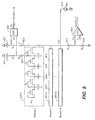
- FIG. 8 illustrates one example of how the pump system can adapt the pump circuits operation based upon the regulation control signals.
- FIG. 8 again shows a voltage comparison section and a current determination section, where the corresponding elements are similarly numbered, and with the output supplying Vout to the load 837 .
- the routing elements such as shown schematically in FIG. 7 , are omitted here for simplicity.
- the pump circuit includes multiple branches, Branch 0 801 - 0 , Branch 1 801 - 1 , . . . Branch N 801 -N. Only the structure of the first branch is shown explicitly and is again shown as a four stage Dickson-type pump.
- the pump strength (or number of branches) can be adjusted dynamically based on Code[n-1,0], as well as, or instead of, just the usual output voltage-based regulation. Only needed branches are enabled to achieve the desired performance for the optimal current consumption, power consumption and output ripple.
- FIG. 9 illustrates other examples of how the pump system can adapt the pump circuits operation based upon the regulation control signals.
- FIG. 9 again shows a voltage comparison section and a current determination section, where the corresponding elements are similarly numbered, and with the output supplying Vout to the load 937 .
- the pump circuit 901 is here taken as a single branch, four stage Dickson type pump, the capacitors being driven by the non-overlapping clock signals phi 1 and phi 2 shown at left.
- the clock signals have a period of tosc (and frequency of 1/tosc) of amplitude Vclock.
- the clock generator is not explicitly shown, but can be taken as externally supplied or part of the charge pump system. For example, FIG.
- the pump circuit can be adapted so that the clock frequency, the clock amplitude, or both can be dynamically adjusted to minimize the power consumption and ripple on output of pump.
- the regulation control signals can be used to vary the change pump operation in other ways, such as altering the number of active stages in a branch, or branches, for example. Further, it should be noted that these different ways of having the charge pump adapt its behavior are largely complimentary and can be variously combined. In any of these cases, the sensing of the current flowing through the pump give one more degree of freedom to be able to adjust pump parameters.
Landscapes
- Engineering & Computer Science (AREA)
- Power Engineering (AREA)
- Dc-Dc Converters (AREA)
Abstract
Description
Claims (26)
Priority Applications (1)
| Application Number | Priority Date | Filing Date | Title |
|---|---|---|---|
| US12/506,998 US7973592B2 (en) | 2009-07-21 | 2009-07-21 | Charge pump with current based regulation |
Applications Claiming Priority (1)
| Application Number | Priority Date | Filing Date | Title |
|---|---|---|---|
| US12/506,998 US7973592B2 (en) | 2009-07-21 | 2009-07-21 | Charge pump with current based regulation |
Publications (2)
| Publication Number | Publication Date |
|---|---|
| US20110018615A1 US20110018615A1 (en) | 2011-01-27 |
| US7973592B2 true US7973592B2 (en) | 2011-07-05 |
Family
ID=43496761
Family Applications (1)
| Application Number | Title | Priority Date | Filing Date |
|---|---|---|---|
| US12/506,998 Expired - Fee Related US7973592B2 (en) | 2009-07-21 | 2009-07-21 | Charge pump with current based regulation |
Country Status (1)
| Country | Link |
|---|---|
| US (1) | US7973592B2 (en) |
Cited By (42)
| Publication number | Priority date | Publication date | Assignee | Title |
|---|---|---|---|---|
| US20120230071A1 (en) * | 2011-03-10 | 2012-09-13 | Semiconductor Components Industries, Llc | Power supply circuit system |
| US8294509B2 (en) | 2010-12-20 | 2012-10-23 | Sandisk Technologies Inc. | Charge pump systems with reduction in inefficiencies due to charge sharing between capacitances |
| US8305807B2 (en) | 2010-07-09 | 2012-11-06 | Sandisk Technologies Inc. | Detection of broken word-lines in memory arrays |
| US8339183B2 (en) | 2009-07-24 | 2012-12-25 | Sandisk Technologies Inc. | Charge pump with reduced energy consumption through charge sharing and clock boosting suitable for high voltage word line in flash memories |
| US8339185B2 (en) | 2010-12-20 | 2012-12-25 | Sandisk 3D Llc | Charge pump system that dynamically selects number of active stages |
| US8379454B2 (en) | 2011-05-05 | 2013-02-19 | Sandisk Technologies Inc. | Detection of broken word-lines in memory arrays |
| WO2013036342A1 (en) | 2011-09-09 | 2013-03-14 | Sandisk Technologies Inc. | Charge pump system dynamically reconfigurable for read and program |
| US8400212B1 (en) | 2011-09-22 | 2013-03-19 | Sandisk Technologies Inc. | High voltage charge pump regulation system with fine step adjustment |
| WO2013043269A2 (en) | 2011-09-22 | 2013-03-28 | Sandisk Technologies Inc. | Dynamic switching approach to reduce area and power consumption of high voltage charge pumps |
| US8432732B2 (en) | 2010-07-09 | 2013-04-30 | Sandisk Technologies Inc. | Detection of word-line leakage in memory arrays |
| US8514630B2 (en) | 2010-07-09 | 2013-08-20 | Sandisk Technologies Inc. | Detection of word-line leakage in memory arrays: current based approach |
| US8519780B1 (en) | 2012-02-08 | 2013-08-27 | Freescale Semiconductor, Inc. | Charge pump voltage regulator |
| WO2014042820A1 (en) | 2012-09-14 | 2014-03-20 | Sandisk Technologies Inc. | Circuits for prevention of reverse leakage in vth-cancellation charge pumps |
| WO2014052163A1 (en) | 2012-09-27 | 2014-04-03 | Sandisk Technologies Inc. | Charge pump based over-sampling adc for current detection |
| US8710907B2 (en) | 2008-06-24 | 2014-04-29 | Sandisk Technologies Inc. | Clock generator circuit for a charge pump |
| US8730722B2 (en) | 2012-03-02 | 2014-05-20 | Sandisk Technologies Inc. | Saving of data in cases of word-line to word-line short in memory arrays |
| US8750042B2 (en) | 2011-07-28 | 2014-06-10 | Sandisk Technologies Inc. | Combined simultaneous sensing of multiple wordlines in a post-write read (PWR) and detection of NAND failures |
| US8775901B2 (en) | 2011-07-28 | 2014-07-08 | SanDisk Technologies, Inc. | Data recovery for defective word lines during programming of non-volatile memory arrays |
| US8872552B2 (en) * | 2012-09-29 | 2014-10-28 | Infineon Technologies Austria Ag | High-side semiconductor-switch low-power driving circuit and method |
| US20150002118A1 (en) * | 2013-06-27 | 2015-01-01 | Sandisk Technologies Inc. | Efficient High Voltage Bias Regulation Circuit |
| US9154028B2 (en) | 2013-03-12 | 2015-10-06 | Freescale Semiconductor, Inc. | Apparatus and method for controlling charge pump |
| US9165683B2 (en) | 2013-09-23 | 2015-10-20 | Sandisk Technologies Inc. | Multi-word line erratic programming detection |
| US9202593B1 (en) | 2014-09-02 | 2015-12-01 | Sandisk Technologies Inc. | Techniques for detecting broken word lines in non-volatile memories |
| US9240249B1 (en) | 2014-09-02 | 2016-01-19 | Sandisk Technologies Inc. | AC stress methods to screen out bit line defects |
| US9443612B2 (en) | 2014-07-10 | 2016-09-13 | Sandisk Technologies Llc | Determination of bit line to low voltage signal shorts |
| US9449694B2 (en) | 2014-09-04 | 2016-09-20 | Sandisk Technologies Llc | Non-volatile memory with multi-word line select for defect detection operations |
| US9460809B2 (en) | 2014-07-10 | 2016-10-04 | Sandisk Technologies Llc | AC stress mode to screen out word line to word line shorts |
| US9484086B2 (en) | 2014-07-10 | 2016-11-01 | Sandisk Technologies Llc | Determination of word line to local source line shorts |
| US9514835B2 (en) | 2014-07-10 | 2016-12-06 | Sandisk Technologies Llc | Determination of word line to word line shorts between adjacent blocks |
| US9520776B1 (en) | 2015-09-18 | 2016-12-13 | Sandisk Technologies Llc | Selective body bias for charge pump transfer switches |
| US9647536B2 (en) | 2015-07-28 | 2017-05-09 | Sandisk Technologies Llc | High voltage generation using low voltage devices |
| US9659666B2 (en) | 2015-08-31 | 2017-05-23 | Sandisk Technologies Llc | Dynamic memory recovery at the sub-block level |
| US9698676B1 (en) | 2016-03-11 | 2017-07-04 | Sandisk Technologies Llc | Charge pump based over-sampling with uniform step size for current detection |
| US9755506B2 (en) | 2014-12-11 | 2017-09-05 | International Business Machines Corporation | Efficient voltage conversion |
| US9810723B2 (en) | 2012-09-27 | 2017-11-07 | Sandisk Technologies Llc | Charge pump based over-sampling ADC for current detection |
| US9831852B2 (en) | 2015-08-31 | 2017-11-28 | Texas Instruments Incorporated | Methods and apparatus for a configurable high-side NMOS gate control with improved gate to source voltage regulation |
| US9917507B2 (en) | 2015-05-28 | 2018-03-13 | Sandisk Technologies Llc | Dynamic clock period modulation scheme for variable charge pump load currents |
| US10242748B2 (en) * | 2010-11-01 | 2019-03-26 | Toshiba Memory Corporation | Voltage generation circuit which is capable of executing high-speed boost operation |
| US10491114B1 (en) * | 2018-12-21 | 2019-11-26 | Nxp B.V. | Output regulated charge pump |
| US10680517B1 (en) * | 2019-04-10 | 2020-06-09 | Yangtze Memory Technologies Co., Ltd. | Reconfigurable voltage regulator |
| US10985653B1 (en) * | 2020-03-20 | 2021-04-20 | Infineon Technologies Ag | Charge pump converter and control method |
| US11586869B2 (en) | 2020-05-01 | 2023-02-21 | Nxp B.V. | RFID transponder and method of operating an RFID transponder |
Families Citing this family (9)
| Publication number | Priority date | Publication date | Assignee | Title |
|---|---|---|---|---|
| US8106701B1 (en) | 2010-09-30 | 2012-01-31 | Sandisk Technologies Inc. | Level shifter with shoot-through current isolation |
| US8537593B2 (en) | 2011-04-28 | 2013-09-17 | Sandisk Technologies Inc. | Variable resistance switch suitable for supplying high voltage to drive load |
| US8395434B1 (en) | 2011-10-05 | 2013-03-12 | Sandisk Technologies Inc. | Level shifter with negative voltage capability |
| US8867281B2 (en) * | 2013-03-15 | 2014-10-21 | Silicon Storage Technology, Inc. | Hybrid chargepump and regulation means and method for flash memory device |
| US9330776B2 (en) | 2014-08-14 | 2016-05-03 | Sandisk Technologies Inc. | High voltage step down regulator with breakdown protection |
| KR101902542B1 (en) * | 2016-12-29 | 2018-09-28 | 주식회사 현대케피코 | Ejector for recirculation device of vaporized fuel |
| US10673321B2 (en) | 2017-11-27 | 2020-06-02 | Marvell Asia Pte., Ltd. | Charge pump circuit with built-in-retry |
| KR102545174B1 (en) * | 2018-10-05 | 2023-06-19 | 삼성전자주식회사 | Memory device having charge pump circuit |
| US11069415B2 (en) | 2018-10-05 | 2021-07-20 | Samsung Electronics Co., Ltd. | Memory device including charge pump circuit |
Citations (139)
| Publication number | Priority date | Publication date | Assignee | Title |
|---|---|---|---|---|
| US3697860A (en) | 1971-03-15 | 1972-10-10 | Westinghouse Electric Corp | Dc static switch circuit with a main switch device and a power sharing circuit portion |
| US4511811A (en) | 1982-02-08 | 1985-04-16 | Seeq Technology, Inc. | Charge pump for providing programming voltage to the word lines in a semiconductor memory array |
| US4583157A (en) | 1985-02-08 | 1986-04-15 | At&T Bell Laboratories | Integrated circuit having a variably boosted node |
| US4636748A (en) | 1985-06-26 | 1987-01-13 | Data General Corporation | Charge pump for use in a phase-locked loop |
| US4736121A (en) | 1985-09-10 | 1988-04-05 | Sos Microelettronica S.p.A. | Charge pump circuit for driving N-channel MOS transistors |
| US4888738A (en) | 1988-06-29 | 1989-12-19 | Seeq Technology | Current-regulated, voltage-regulated erase circuit for EEPROM memory |
| US5168174A (en) | 1991-07-12 | 1992-12-01 | Texas Instruments Incorporated | Negative-voltage charge pump with feedback control |
| US5175706A (en) | 1989-12-07 | 1992-12-29 | Sgs-Thomson Microelectronics S.A. | Programming voltage generator circuit for programmable memory |
| US5263000A (en) | 1992-10-22 | 1993-11-16 | Advanced Micro Devices, Inc. | Drain power supply |
| EP0382929B1 (en) | 1989-02-16 | 1994-08-31 | Kabushiki Kaisha Toshiba | Voltage regulator circuit |
| US5392205A (en) | 1991-11-07 | 1995-02-21 | Motorola, Inc. | Regulated charge pump and method therefor |
| US5436587A (en) | 1993-11-24 | 1995-07-25 | Sundisk Corporation | Charge pump circuit with exponetral multiplication |
| US5483434A (en) | 1992-01-14 | 1996-01-09 | Seesink; Petrus H. | High voltage generator having output current control |
| US5508971A (en) | 1994-10-17 | 1996-04-16 | Sandisk Corporation | Programmable power generation circuit for flash EEPROM memory systems |
| US5521547A (en) | 1992-06-24 | 1996-05-28 | Nec Corporation | Boost voltage generating circuit |
| US5563779A (en) | 1994-12-05 | 1996-10-08 | Motorola, Inc. | Method and apparatus for a regulated supply on an integrated circuit |
| US5596532A (en) | 1995-10-18 | 1997-01-21 | Sandisk Corporation | Flash EEPROM self-adaptive voltage generation circuit operative within a continuous voltage source range |
| US5625544A (en) | 1996-04-25 | 1997-04-29 | Programmable Microelectronics Corp. | Charge pump |
| US5734286A (en) | 1993-05-19 | 1998-03-31 | Kabushiki Kaisha Toshiba | Driving device of charge pump circuit and driving pulse generation method thereof |
| US5818766A (en) | 1997-03-05 | 1998-10-06 | Integrated Silicon Solution Inc. | Drain voltage pump circuit for nonvolatile memory device |
| US5943226A (en) | 1997-02-27 | 1999-08-24 | Lg Semicon Co., Ltd. | Bootstrap charge pump circuit |
| US5945870A (en) | 1996-07-18 | 1999-08-31 | Altera Corporation | Voltage ramp rate control circuit |
| US5969565A (en) | 1996-05-17 | 1999-10-19 | Nec Corporation | Voltage booster circuit |
| US5973546A (en) | 1996-06-27 | 1999-10-26 | Advanced Micro Devices, Inc. | Charge pump circuit architecture |
| EP0780515B1 (en) | 1995-12-21 | 1999-11-03 | BWG Butzbacher Weichenbau Gesellschaft mbH & Co. KG | Device for holding down a rail |
| US5982222A (en) | 1995-12-30 | 1999-11-09 | Samsung Electronics, Co., Ltd. | High voltage generating circuit for a semiconductor memory device |
| US6008690A (en) | 1997-06-11 | 1999-12-28 | Nec Corporation | Booster circuit |
| US6018264A (en) | 1998-02-11 | 2000-01-25 | Lg Semicon Co., Ltd. | Pumping circuit with amplitude limited to prevent an over pumping for semiconductor device |
| US6023187A (en) | 1997-12-23 | 2000-02-08 | Mitsubishi Semiconductor America, Inc. | Voltage pump for integrated circuit and operating method thereof |
| US6026002A (en) | 1996-03-28 | 2000-02-15 | Siemens Aktiengesellschaft | Circuit configuration for supplying an electronic load circuit |
| US6104225A (en) | 1997-04-21 | 2000-08-15 | Fujitsu Limited | Semiconductor device using complementary clock and signal input state detection circuit used for the same |
| US6107862A (en) | 1997-02-28 | 2000-08-22 | Seiko Instruments Inc. | Charge pump circuit |
| US6134145A (en) | 1998-06-23 | 2000-10-17 | Sandisk Corporation | High data rate write process for non-volatile flash memories |
| US6154088A (en) | 1996-07-18 | 2000-11-28 | Micron Technology, Inc. | Clocking scheme and charge transfer switch for increasing the efficiency of a charge pump or other circuit |
| WO2001006336A1 (en) | 1999-07-15 | 2001-01-25 | Maxim Integrated Products, Inc. | Pulse frequency operation of regulated charge pumps |
| US6188590B1 (en) | 1996-12-18 | 2001-02-13 | Macronix International Co., Ltd. | Regulator system for charge pump circuits |
| US6198645B1 (en) | 1998-07-02 | 2001-03-06 | National Semiconductor Corporation | Buck and boost switched capacitor gain stage with optional shared rest state |
| US6208198B1 (en) | 1998-10-27 | 2001-03-27 | Hyundai Electronics Industries Co., Ltd. | Drain voltage pumping circuit |
| US6249445B1 (en) | 1999-02-15 | 2001-06-19 | Nec Corporation | Booster including charge pumping circuit with its electric power consumption reduced and method of operating the same |
| US6249898B1 (en) | 1998-06-30 | 2001-06-19 | Synopsys, Inc. | Method and system for reliability analysis of CMOS VLSI circuits based on stage partitioning and node activities |
| US6285622B1 (en) | 1999-10-29 | 2001-09-04 | Mitsubishi Denki Kabushiki Kaisha | Semiconductor device |
| US6314025B1 (en) | 1998-06-23 | 2001-11-06 | Sandisk Corporation | High data rate write process for non-volatile flash memories |
| US6320796B1 (en) | 2000-11-10 | 2001-11-20 | Marvell International, Ltd. | Variable slope charge pump control |
| US6329869B1 (en) | 1999-05-19 | 2001-12-11 | Nec Corporation | Semiconductor device with less influence of noise |
| US6344984B1 (en) | 1999-09-03 | 2002-02-05 | Nec Corporation | Voltage multiplier having an intermediate tap |
| US6344959B1 (en) | 1998-05-01 | 2002-02-05 | Unitrode Corporation | Method for sensing the output voltage of a charge pump circuit without applying a load to the output stage |
| US20020014908A1 (en) | 1998-12-21 | 2002-02-07 | Christl Lauterbach | Device for voltage multiplication with high efficiency, combination of the device with a battery-operated apparatus, and low-power loss generation of a programming voltage |
| US6359798B1 (en) | 2000-12-08 | 2002-03-19 | Samsung Electronics Co., Ltd. | Charge pump voltage converter |
| US6370075B1 (en) | 1998-06-30 | 2002-04-09 | Sandisk Corporation | Charge pump circuit adjustable in response to an external voltage source |
| US6400202B1 (en) | 2000-02-10 | 2002-06-04 | International Business Machines Corporation | Programmable delay element and synchronous DRAM using the same |
| US6404274B1 (en) | 1998-04-09 | 2002-06-11 | Kabushiki Kaisha Toshiba | Internal voltage generating circuit capable of generating variable multi-level voltages |
| US20020075706A1 (en) | 1990-04-06 | 2002-06-20 | Mosaid Technologies Incorporated | Boosted voltage supply |
| US6424570B1 (en) | 2001-06-26 | 2002-07-23 | Advanced Micro Devices, Inc. | Modulated charge pump with uses an analog to digital converter to compensate for supply voltage variations |
| US6445243B2 (en) | 2000-05-10 | 2002-09-03 | Sanyo Electric Co., Ltd. | Charge-pump circuit and control method thereof |
| US6456170B1 (en) | 1999-06-01 | 2002-09-24 | Fujitsu Limited | Comparator and voltage controlled oscillator circuit |
| US20020140463A1 (en) | 2001-03-15 | 2002-10-03 | Paul Cheung | Programmable soft-start control for charge pump |
| US6476666B1 (en) | 2001-05-30 | 2002-11-05 | Alliance Semiconductor Corporation | Bootstrapped charge pump |
| US6486728B2 (en) | 2001-03-16 | 2002-11-26 | Matrix Semiconductor, Inc. | Multi-stage charge pump |
| US6518830B2 (en) | 2000-08-22 | 2003-02-11 | Stmicroelectronics S.R.L. | High efficiency electronic circuit for generating and regulating a supply voltage |
| US6525614B2 (en) | 2000-11-17 | 2003-02-25 | Sanyo Electric Co., Ltd. | Voltage boost system having feedback control |
| US6525949B1 (en) | 2000-12-22 | 2003-02-25 | Matrix Semiconductor, Inc. | Charge pump circuit |
| US6531792B2 (en) | 2001-04-10 | 2003-03-11 | Fujitsu Limited | DC-DC converter and storage apparatus |
| US6538930B2 (en) * | 2001-01-09 | 2003-03-25 | Mitsubishi Denki Kabushiki Kaisha | Charge pump circuit for generating positive and negative voltage with reverse current prevention circuit and a nonvolatile memory using the same |
| US6545529B2 (en) | 2000-05-02 | 2003-04-08 | Hynix Semiconductor Inc. | High voltage generating circuit |
| US6577535B2 (en) | 2001-02-16 | 2003-06-10 | Sandisk Corporation | Method and system for distributed power generation in multi-chip memory systems |
| US20030128560A1 (en) | 2002-01-10 | 2003-07-10 | Saiki William John | High voltage generation and regulation system for digital multilevel nonvolatile memory |
| US6606267B2 (en) | 1998-06-23 | 2003-08-12 | Sandisk Corporation | High data rate write process for non-volatile flash memories |
| US20030214346A1 (en) | 2002-02-25 | 2003-11-20 | Stmicroelectronics S.R.I. | Charge pump for negative voltages |
| US6724241B1 (en) | 2002-10-25 | 2004-04-20 | Atmel Corporation | Variable charge pump circuit with dynamic load |
| US6734718B1 (en) | 2002-12-23 | 2004-05-11 | Sandisk Corporation | High voltage ripple reduction |
| US6781440B2 (en) | 2002-02-18 | 2004-08-24 | Winbond Electronics Corp. | Charge pump circuit with voltage multiplier for boosting clock signal and method thereof |
| US6798274B2 (en) | 2002-03-27 | 2004-09-28 | Sanyo Electric Co., Ltd. | Booster and imaging device using booster |
| US6801454B2 (en) | 2002-10-01 | 2004-10-05 | Sandisk Corporation | Voltage generation circuitry having temperature compensation |
| US6834001B2 (en) | 2001-09-26 | 2004-12-21 | Sanyo Electric Co., Ltd. | Multi-stage switched capacitor DC-DC converter |
| US6859091B1 (en) | 2003-09-18 | 2005-02-22 | Maxim Integrated Products, Inc. | Continuous linear regulated zero dropout charge pump with high efficiency load predictive clocking scheme |
| US6878981B2 (en) * | 2003-03-20 | 2005-04-12 | Tower Semiconductor Ltd. | Triple-well charge pump stage with no threshold voltage back-bias effect |
| US20050093614A1 (en) | 2003-10-30 | 2005-05-05 | Dong-Uk Lee | Multi stage voltage pump circuit |
| US6891764B2 (en) | 2003-04-11 | 2005-05-10 | Intel Corporation | Apparatus and method to read a nonvolatile memory |
| US6894554B2 (en) | 2002-01-17 | 2005-05-17 | Seiko Epson Corporation | Step-up circuits |
| US6922096B2 (en) | 2003-08-07 | 2005-07-26 | Sandisk Corporation | Area efficient charge pump |
| US20050195017A1 (en) | 2004-03-03 | 2005-09-08 | Tien-Tzu Chen | High efficiency charge pump with prevention from reverse current |
| US20050248386A1 (en) | 2004-05-10 | 2005-11-10 | Sandisk Corporation | Four phase charge pump operable without phase overlap with improved efficiency |
| US6975135B1 (en) | 2002-12-10 | 2005-12-13 | Altera Corporation | Universally programmable output buffer |
| US6990031B2 (en) | 2001-09-03 | 2006-01-24 | Elpida Memory, Inc. | Semiconductor memory device control method and semiconductor memory device |
| US7002381B1 (en) | 2001-12-11 | 2006-02-21 | Advanced Micro Devices, Inc. | Switched-capacitor controller to control the rise times of on-chip generated high voltages |
| US7023260B2 (en) | 2003-06-30 | 2006-04-04 | Matrix Semiconductor, Inc. | Charge pump circuit incorporating corresponding parallel charge pump stages and method therefor |
| US20060114053A1 (en) | 2004-11-30 | 2006-06-01 | Renesas Technology Corp. | Charge-pump-type power supply circuit |
| US7116154B2 (en) | 2003-08-06 | 2006-10-03 | Spansion Llc | Low power charge pump |
| US7120051B2 (en) | 2004-12-14 | 2006-10-10 | Sandisk Corporation | Pipelined programming of non-volatile memories using early data |
| US7129759B2 (en) * | 2004-02-03 | 2006-10-31 | Nec Electronics Corporation | Integrated circuit including an overvoltage protection circuit |
| US20060244518A1 (en) | 2005-04-29 | 2006-11-02 | Hynix Semiconductor Inc. | Internal voltage generator |
| US7135911B2 (en) | 2000-05-24 | 2006-11-14 | Kabushiki Kaisha Toshiba | Potential detector and semiconductor integrated circuit |
| US7135910B2 (en) | 2002-09-27 | 2006-11-14 | Sandisk Corporation | Charge pump with fibonacci number multiplication |
| US20070001745A1 (en) | 2005-06-29 | 2007-01-04 | Chih-Jen Yen | Charge pump for generating arbitrary voltage levels |
| US20070069805A1 (en) | 2005-09-29 | 2007-03-29 | Hynix Semiconductor Inc. | Internal voltage generating circuit |
| US7208996B2 (en) | 2004-03-26 | 2007-04-24 | Sanyo Electric Co., Ltd. | Charge pump circuit |
| US7224591B2 (en) * | 2005-02-24 | 2007-05-29 | Sharp Kabushiki Kaisha | Charge pump DC/DC converter circuit |
| US7227780B2 (en) | 2004-11-30 | 2007-06-05 | Spansion Llc | Semiconductor device and control method thereof |
| US20070126494A1 (en) | 2005-12-06 | 2007-06-07 | Sandisk Corporation | Charge pump having shunt diode for improved operating efficiency |
| US20070139099A1 (en) | 2005-12-16 | 2007-06-21 | Sandisk Corporation | Charge pump regulation control for improved power efficiency |
| US20070139100A1 (en) | 2005-12-16 | 2007-06-21 | Sandisk Corporation | Voltage regulation with active supplemental current for output stabilization |
| US7239192B2 (en) | 2003-08-06 | 2007-07-03 | Stmicroelectronics Sa | Self-reparable device to generate a high voltage, and method for repairing a device to generate a high voltage |
| US7253676B2 (en) | 2003-12-25 | 2007-08-07 | Kabushiki Kaisha Toshiba | Semiconductor device and driving method of semiconductor device |
| US7259612B2 (en) | 2005-06-28 | 2007-08-21 | Atmel Corporation | Efficient charge pump for a wide range of supply voltages |
| US20070222498A1 (en) | 2006-03-24 | 2007-09-27 | Freescale Semiconductor Inc. | Slew rate control of a charge pump |
| US7276960B2 (en) | 2005-07-18 | 2007-10-02 | Dialog Semiconductor Gmbh | Voltage regulated charge pump with regulated charge current into the flying capacitor |
| US20070229149A1 (en) | 2006-03-30 | 2007-10-04 | Sandisk Corporation | Voltage regulator having high voltage protection |
| US20080024096A1 (en) | 2006-07-31 | 2008-01-31 | Sandisk Corporation | Hybrid charge pump regulation |
| US7345335B2 (en) | 2004-06-09 | 2008-03-18 | Kabushiki Kaisha Toshiba | Semiconductor integrated circuit, booster circuitry, and non-volatile semiconductor memory device |
| US7368979B2 (en) | 2006-09-19 | 2008-05-06 | Sandisk Corporation | Implementation of output floating scheme for hv charge pumps |
| US20080111604A1 (en) * | 2005-03-17 | 2008-05-15 | Boerstler David W | Digital circuit to measure and/or correct duty cycles |
| US20080116963A1 (en) | 2006-11-20 | 2008-05-22 | Hynix Semiconductor Inc. | Clock control circuit and voltage pumping device using the same |
| US20080157852A1 (en) | 2006-12-29 | 2008-07-03 | Sandisk Corporation | Unified voltage generation apparatus with improved power efficiency |
| US20080157859A1 (en) | 2006-12-29 | 2008-07-03 | Sandisk Corporation | Unified voltage generation method with improved power efficiency |
| DE102007026290A1 (en) | 2006-12-28 | 2008-07-03 | Samsung Electronics Co., Ltd., Suwon | High voltage generating circuit, has regulator generating high voltage measuring current for measuring high voltage depending on level of high voltage, for controlling control signal, and for generating activation signal |
| US7397677B1 (en) | 2006-02-08 | 2008-07-08 | National Semiconductor Corporation | Apparatus and method for charge pump control with adjustable series resistance |
| US20080198662A1 (en) | 2007-02-20 | 2008-08-21 | Nima Mokhlesi | Dynamic verify based on threshold voltage distribution |
| US20080218134A1 (en) | 2007-03-08 | 2008-09-11 | Matsushita Electric Industrial Co., Ltd. | Power supply apparatus |
| US20080239802A1 (en) | 2007-03-30 | 2008-10-02 | Tyler Thorp | Device with Load-Based Voltage Generation |
| US20080239856A1 (en) | 2007-03-30 | 2008-10-02 | Tyler Thorp | Method for Load-Based Voltage Generation |
| US7443735B2 (en) | 2006-12-22 | 2008-10-28 | Sandisk Corporation | Method of reducing wordline recovery time |
| US20080278222A1 (en) | 2006-07-19 | 2008-11-13 | Stmicroelectronics S.R.I. | Charge pump circuit |
| US7463521B2 (en) | 2005-04-01 | 2008-12-09 | Sandisk Corporation | Method for non-volatile memory with managed execution of cached data |
| US7468628B2 (en) | 2004-11-08 | 2008-12-23 | Hynix Semiconductor Inc. | Internal voltage generators for semiconductor memory device |
| US20090033306A1 (en) | 2007-08-02 | 2009-02-05 | Toru Tanzawa | Voltage trimming |
| US20090051413A1 (en) | 2007-08-20 | 2009-02-26 | Taiwan Semiconductor Manufacturing Company, Ltd. | Apparatus and method for increasing charge pump efficiency |
| US20090058507A1 (en) | 2007-08-28 | 2009-03-05 | Prajit Nandi | Bottom Plate Regulated Charge Pump |
| US20090058506A1 (en) | 2007-08-28 | 2009-03-05 | Prajit Nandi | Bottom Plate Regulation of Charge Pumps |
| US20090091366A1 (en) | 2007-10-09 | 2009-04-09 | Hynix Semiconductor, Inc. | Voltage generator of semiconductor integrated circuit |
| US7521978B2 (en) | 2005-11-02 | 2009-04-21 | Hynix Semiconductor Inc. | Clock driver |
| US20090121780A1 (en) | 2007-11-12 | 2009-05-14 | Macronix International Co., Ltd. | Multiple-stage charge pump with charge recycle circuit |
| US20090153232A1 (en) | 2007-05-25 | 2009-06-18 | Atmel Corporation | Low voltage charge pump |
| US20090153230A1 (en) | 2007-12-12 | 2009-06-18 | Feng Pan | Low Voltage Charge Pump with Regulation |
| US20090153231A1 (en) | 2007-12-12 | 2009-06-18 | Feng Pan | Diode Connected Regulation of Charge Pumps |
| US20090167418A1 (en) | 2007-10-24 | 2009-07-02 | Vijay Raghavan | Supply Regulated Charge Pump System |
| US7579903B2 (en) | 2005-08-03 | 2009-08-25 | Nec Electronics Corporation | Power-source potential control circuit and method of trimming power-source potential |
| US20090219077A1 (en) | 2008-02-29 | 2009-09-03 | Stefano Pietri | Voltage multiplier with improved efficiency |
| US7671572B2 (en) | 2006-04-07 | 2010-03-02 | Samsung Electronics Co. Ltd. | Voltage boost circuit and voltage boosting method using voltage boost clock signal with varying frequency |
| US20100244935A1 (en) | 2007-11-05 | 2010-09-30 | Electronics And Telecommunications Research Institute | High-voltage cmos charge pump |
-
2009
- 2009-07-21 US US12/506,998 patent/US7973592B2/en not_active Expired - Fee Related
Patent Citations (158)
| Publication number | Priority date | Publication date | Assignee | Title |
|---|---|---|---|---|
| US3697860A (en) | 1971-03-15 | 1972-10-10 | Westinghouse Electric Corp | Dc static switch circuit with a main switch device and a power sharing circuit portion |
| US4511811A (en) | 1982-02-08 | 1985-04-16 | Seeq Technology, Inc. | Charge pump for providing programming voltage to the word lines in a semiconductor memory array |
| US4583157A (en) | 1985-02-08 | 1986-04-15 | At&T Bell Laboratories | Integrated circuit having a variably boosted node |
| US4636748A (en) | 1985-06-26 | 1987-01-13 | Data General Corporation | Charge pump for use in a phase-locked loop |
| US4736121A (en) | 1985-09-10 | 1988-04-05 | Sos Microelettronica S.p.A. | Charge pump circuit for driving N-channel MOS transistors |
| US4888738A (en) | 1988-06-29 | 1989-12-19 | Seeq Technology | Current-regulated, voltage-regulated erase circuit for EEPROM memory |
| EP0382929B1 (en) | 1989-02-16 | 1994-08-31 | Kabushiki Kaisha Toshiba | Voltage regulator circuit |
| US5175706A (en) | 1989-12-07 | 1992-12-29 | Sgs-Thomson Microelectronics S.A. | Programming voltage generator circuit for programmable memory |
| US20020075706A1 (en) | 1990-04-06 | 2002-06-20 | Mosaid Technologies Incorporated | Boosted voltage supply |
| US5168174A (en) | 1991-07-12 | 1992-12-01 | Texas Instruments Incorporated | Negative-voltage charge pump with feedback control |
| US5392205A (en) | 1991-11-07 | 1995-02-21 | Motorola, Inc. | Regulated charge pump and method therefor |
| US5483434A (en) | 1992-01-14 | 1996-01-09 | Seesink; Petrus H. | High voltage generator having output current control |
| US5521547A (en) | 1992-06-24 | 1996-05-28 | Nec Corporation | Boost voltage generating circuit |
| US5263000A (en) | 1992-10-22 | 1993-11-16 | Advanced Micro Devices, Inc. | Drain power supply |
| US5734286A (en) | 1993-05-19 | 1998-03-31 | Kabushiki Kaisha Toshiba | Driving device of charge pump circuit and driving pulse generation method thereof |
| US5436587A (en) | 1993-11-24 | 1995-07-25 | Sundisk Corporation | Charge pump circuit with exponetral multiplication |
| US5693570A (en) | 1994-10-17 | 1997-12-02 | Sandisk Corporation | Process for manufacturing a programmable power generation circuit for flash EEPROM memory systems |
| US5592420A (en) | 1994-10-17 | 1997-01-07 | Sandisk Corporation | Programmable power generation circuit for flash EEPROM memory systems |
| US5621685A (en) | 1994-10-17 | 1997-04-15 | Sandisk Corporation | Programmable power generation circuit for flash EEPROM memory systems |
| US5508971A (en) | 1994-10-17 | 1996-04-16 | Sandisk Corporation | Programmable power generation circuit for flash EEPROM memory systems |
| US5563825A (en) | 1994-10-17 | 1996-10-08 | Sandisk Corporation | Programmable power generation circuit for flash eeprom memory systems |
| US5568424A (en) | 1994-10-17 | 1996-10-22 | Sandisk Corporation | Programmable power generation circuit for flash EEPROM memory systems |
| US5563779A (en) | 1994-12-05 | 1996-10-08 | Motorola, Inc. | Method and apparatus for a regulated supply on an integrated circuit |
| US5596532A (en) | 1995-10-18 | 1997-01-21 | Sandisk Corporation | Flash EEPROM self-adaptive voltage generation circuit operative within a continuous voltage source range |
| EP0780515B1 (en) | 1995-12-21 | 1999-11-03 | BWG Butzbacher Weichenbau Gesellschaft mbH & Co. KG | Device for holding down a rail |
| US5982222A (en) | 1995-12-30 | 1999-11-09 | Samsung Electronics, Co., Ltd. | High voltage generating circuit for a semiconductor memory device |
| US6026002A (en) | 1996-03-28 | 2000-02-15 | Siemens Aktiengesellschaft | Circuit configuration for supplying an electronic load circuit |
| US5625544A (en) | 1996-04-25 | 1997-04-29 | Programmable Microelectronics Corp. | Charge pump |
| US5969565A (en) | 1996-05-17 | 1999-10-19 | Nec Corporation | Voltage booster circuit |
| US5973546A (en) | 1996-06-27 | 1999-10-26 | Advanced Micro Devices, Inc. | Charge pump circuit architecture |
| US5945870A (en) | 1996-07-18 | 1999-08-31 | Altera Corporation | Voltage ramp rate control circuit |
| US6154088A (en) | 1996-07-18 | 2000-11-28 | Micron Technology, Inc. | Clocking scheme and charge transfer switch for increasing the efficiency of a charge pump or other circuit |
| US6188590B1 (en) | 1996-12-18 | 2001-02-13 | Macronix International Co., Ltd. | Regulator system for charge pump circuits |
| US5943226A (en) | 1997-02-27 | 1999-08-24 | Lg Semicon Co., Ltd. | Bootstrap charge pump circuit |
| US6107862A (en) | 1997-02-28 | 2000-08-22 | Seiko Instruments Inc. | Charge pump circuit |
| US5818766A (en) | 1997-03-05 | 1998-10-06 | Integrated Silicon Solution Inc. | Drain voltage pump circuit for nonvolatile memory device |
| US6104225A (en) | 1997-04-21 | 2000-08-15 | Fujitsu Limited | Semiconductor device using complementary clock and signal input state detection circuit used for the same |
| US6008690A (en) | 1997-06-11 | 1999-12-28 | Nec Corporation | Booster circuit |
| US6023187A (en) | 1997-12-23 | 2000-02-08 | Mitsubishi Semiconductor America, Inc. | Voltage pump for integrated circuit and operating method thereof |
| US6018264A (en) | 1998-02-11 | 2000-01-25 | Lg Semicon Co., Ltd. | Pumping circuit with amplitude limited to prevent an over pumping for semiconductor device |
| US6404274B1 (en) | 1998-04-09 | 2002-06-11 | Kabushiki Kaisha Toshiba | Internal voltage generating circuit capable of generating variable multi-level voltages |
| US6344959B1 (en) | 1998-05-01 | 2002-02-05 | Unitrode Corporation | Method for sensing the output voltage of a charge pump circuit without applying a load to the output stage |
| US6314025B1 (en) | 1998-06-23 | 2001-11-06 | Sandisk Corporation | High data rate write process for non-volatile flash memories |
| US6606267B2 (en) | 1998-06-23 | 2003-08-12 | Sandisk Corporation | High data rate write process for non-volatile flash memories |
| US6944058B2 (en) | 1998-06-23 | 2005-09-13 | Sandisk Corporation | High data rate write process for non-volatile flash memories |
| US6134145A (en) | 1998-06-23 | 2000-10-17 | Sandisk Corporation | High data rate write process for non-volatile flash memories |
| US6249898B1 (en) | 1998-06-30 | 2001-06-19 | Synopsys, Inc. | Method and system for reliability analysis of CMOS VLSI circuits based on stage partitioning and node activities |
| US6556465B2 (en) | 1998-06-30 | 2003-04-29 | Sandisk Corporation | Adjustable circuits for analog or multi-level memory |
| US6760262B2 (en) | 1998-06-30 | 2004-07-06 | Sandisk Corporation | Charge pump circuit adjustable in response to an external voltage source |
| US6370075B1 (en) | 1998-06-30 | 2002-04-09 | Sandisk Corporation | Charge pump circuit adjustable in response to an external voltage source |
| US6198645B1 (en) | 1998-07-02 | 2001-03-06 | National Semiconductor Corporation | Buck and boost switched capacitor gain stage with optional shared rest state |
| US6208198B1 (en) | 1998-10-27 | 2001-03-27 | Hyundai Electronics Industries Co., Ltd. | Drain voltage pumping circuit |
| US20020014908A1 (en) | 1998-12-21 | 2002-02-07 | Christl Lauterbach | Device for voltage multiplication with high efficiency, combination of the device with a battery-operated apparatus, and low-power loss generation of a programming voltage |
| US6249445B1 (en) | 1999-02-15 | 2001-06-19 | Nec Corporation | Booster including charge pumping circuit with its electric power consumption reduced and method of operating the same |
| US6329869B1 (en) | 1999-05-19 | 2001-12-11 | Nec Corporation | Semiconductor device with less influence of noise |
| US6456170B1 (en) | 1999-06-01 | 2002-09-24 | Fujitsu Limited | Comparator and voltage controlled oscillator circuit |
| WO2001006336A1 (en) | 1999-07-15 | 2001-01-25 | Maxim Integrated Products, Inc. | Pulse frequency operation of regulated charge pumps |
| US6344984B1 (en) | 1999-09-03 | 2002-02-05 | Nec Corporation | Voltage multiplier having an intermediate tap |
| US6285622B1 (en) | 1999-10-29 | 2001-09-04 | Mitsubishi Denki Kabushiki Kaisha | Semiconductor device |
| US6400202B1 (en) | 2000-02-10 | 2002-06-04 | International Business Machines Corporation | Programmable delay element and synchronous DRAM using the same |
| US6545529B2 (en) | 2000-05-02 | 2003-04-08 | Hynix Semiconductor Inc. | High voltage generating circuit |
| US6445243B2 (en) | 2000-05-10 | 2002-09-03 | Sanyo Electric Co., Ltd. | Charge-pump circuit and control method thereof |
| US7135911B2 (en) | 2000-05-24 | 2006-11-14 | Kabushiki Kaisha Toshiba | Potential detector and semiconductor integrated circuit |
| US6518830B2 (en) | 2000-08-22 | 2003-02-11 | Stmicroelectronics S.R.L. | High efficiency electronic circuit for generating and regulating a supply voltage |
| US6320796B1 (en) | 2000-11-10 | 2001-11-20 | Marvell International, Ltd. | Variable slope charge pump control |
| US6525614B2 (en) | 2000-11-17 | 2003-02-25 | Sanyo Electric Co., Ltd. | Voltage boost system having feedback control |
| US6359798B1 (en) | 2000-12-08 | 2002-03-19 | Samsung Electronics Co., Ltd. | Charge pump voltage converter |
| US6525949B1 (en) | 2000-12-22 | 2003-02-25 | Matrix Semiconductor, Inc. | Charge pump circuit |
| US6538930B2 (en) * | 2001-01-09 | 2003-03-25 | Mitsubishi Denki Kabushiki Kaisha | Charge pump circuit for generating positive and negative voltage with reverse current prevention circuit and a nonvolatile memory using the same |
| US6577535B2 (en) | 2001-02-16 | 2003-06-10 | Sandisk Corporation | Method and system for distributed power generation in multi-chip memory systems |
| US20020140463A1 (en) | 2001-03-15 | 2002-10-03 | Paul Cheung | Programmable soft-start control for charge pump |
| US6486728B2 (en) | 2001-03-16 | 2002-11-26 | Matrix Semiconductor, Inc. | Multi-stage charge pump |
| US6531792B2 (en) | 2001-04-10 | 2003-03-11 | Fujitsu Limited | DC-DC converter and storage apparatus |
| US6476666B1 (en) | 2001-05-30 | 2002-11-05 | Alliance Semiconductor Corporation | Bootstrapped charge pump |
| US6424570B1 (en) | 2001-06-26 | 2002-07-23 | Advanced Micro Devices, Inc. | Modulated charge pump with uses an analog to digital converter to compensate for supply voltage variations |
| US6990031B2 (en) | 2001-09-03 | 2006-01-24 | Elpida Memory, Inc. | Semiconductor memory device control method and semiconductor memory device |
| US6834001B2 (en) | 2001-09-26 | 2004-12-21 | Sanyo Electric Co., Ltd. | Multi-stage switched capacitor DC-DC converter |
| US7002381B1 (en) | 2001-12-11 | 2006-02-21 | Advanced Micro Devices, Inc. | Switched-capacitor controller to control the rise times of on-chip generated high voltages |
| US20030128560A1 (en) | 2002-01-10 | 2003-07-10 | Saiki William John | High voltage generation and regulation system for digital multilevel nonvolatile memory |
| US6894554B2 (en) | 2002-01-17 | 2005-05-17 | Seiko Epson Corporation | Step-up circuits |
| US6781440B2 (en) | 2002-02-18 | 2004-08-24 | Winbond Electronics Corp. | Charge pump circuit with voltage multiplier for boosting clock signal and method thereof |
| US6819162B2 (en) | 2002-02-25 | 2004-11-16 | Stmicroelectronics S.R.L. | Charge pump for negative voltages |
| US20030214346A1 (en) | 2002-02-25 | 2003-11-20 | Stmicroelectronics S.R.I. | Charge pump for negative voltages |
| US6798274B2 (en) | 2002-03-27 | 2004-09-28 | Sanyo Electric Co., Ltd. | Booster and imaging device using booster |
| US7135910B2 (en) | 2002-09-27 | 2006-11-14 | Sandisk Corporation | Charge pump with fibonacci number multiplication |
| US6801454B2 (en) | 2002-10-01 | 2004-10-05 | Sandisk Corporation | Voltage generation circuitry having temperature compensation |
| US6724241B1 (en) | 2002-10-25 | 2004-04-20 | Atmel Corporation | Variable charge pump circuit with dynamic load |
| US6975135B1 (en) | 2002-12-10 | 2005-12-13 | Altera Corporation | Universally programmable output buffer |
| US6734718B1 (en) | 2002-12-23 | 2004-05-11 | Sandisk Corporation | High voltage ripple reduction |
| US7116155B2 (en) | 2002-12-23 | 2006-10-03 | Sandisk Corporation | High voltage ripple reduction and substrate protection |
| US6878981B2 (en) * | 2003-03-20 | 2005-04-12 | Tower Semiconductor Ltd. | Triple-well charge pump stage with no threshold voltage back-bias effect |
| US6891764B2 (en) | 2003-04-11 | 2005-05-10 | Intel Corporation | Apparatus and method to read a nonvolatile memory |
| US7023260B2 (en) | 2003-06-30 | 2006-04-04 | Matrix Semiconductor, Inc. | Charge pump circuit incorporating corresponding parallel charge pump stages and method therefor |
| US7239192B2 (en) | 2003-08-06 | 2007-07-03 | Stmicroelectronics Sa | Self-reparable device to generate a high voltage, and method for repairing a device to generate a high voltage |
| US7116154B2 (en) | 2003-08-06 | 2006-10-03 | Spansion Llc | Low power charge pump |
| US6922096B2 (en) | 2003-08-07 | 2005-07-26 | Sandisk Corporation | Area efficient charge pump |
| US20050237103A1 (en) | 2003-08-07 | 2005-10-27 | Raul-Adrian Cernea | Area efficient charge pump |
| US7113023B2 (en) | 2003-08-07 | 2006-09-26 | Sandisk Corporation | Area efficient charge pump |
| US6859091B1 (en) | 2003-09-18 | 2005-02-22 | Maxim Integrated Products, Inc. | Continuous linear regulated zero dropout charge pump with high efficiency load predictive clocking scheme |
| US20050093614A1 (en) | 2003-10-30 | 2005-05-05 | Dong-Uk Lee | Multi stage voltage pump circuit |
| US7253676B2 (en) | 2003-12-25 | 2007-08-07 | Kabushiki Kaisha Toshiba | Semiconductor device and driving method of semiconductor device |
| US7129759B2 (en) * | 2004-02-03 | 2006-10-31 | Nec Electronics Corporation | Integrated circuit including an overvoltage protection circuit |
| US6995603B2 (en) | 2004-03-03 | 2006-02-07 | Aimtron Technology Corp. | High efficiency charge pump with prevention from reverse current |
| US20050195017A1 (en) | 2004-03-03 | 2005-09-08 | Tien-Tzu Chen | High efficiency charge pump with prevention from reverse current |
| US7208996B2 (en) | 2004-03-26 | 2007-04-24 | Sanyo Electric Co., Ltd. | Charge pump circuit |
| US20050248386A1 (en) | 2004-05-10 | 2005-11-10 | Sandisk Corporation | Four phase charge pump operable without phase overlap with improved efficiency |
| US7030683B2 (en) | 2004-05-10 | 2006-04-18 | Sandisk Corporation | Four phase charge pump operable without phase overlap with improved efficiency |
| US7345335B2 (en) | 2004-06-09 | 2008-03-18 | Kabushiki Kaisha Toshiba | Semiconductor integrated circuit, booster circuitry, and non-volatile semiconductor memory device |
| US7468628B2 (en) | 2004-11-08 | 2008-12-23 | Hynix Semiconductor Inc. | Internal voltage generators for semiconductor memory device |
| US20060114053A1 (en) | 2004-11-30 | 2006-06-01 | Renesas Technology Corp. | Charge-pump-type power supply circuit |
| US7227780B2 (en) | 2004-11-30 | 2007-06-05 | Spansion Llc | Semiconductor device and control method thereof |
| US7120051B2 (en) | 2004-12-14 | 2006-10-10 | Sandisk Corporation | Pipelined programming of non-volatile memories using early data |
| US7345928B2 (en) | 2004-12-14 | 2008-03-18 | Sandisk Corporation | Data recovery methods in multi-state memory after program fail |
| US7224591B2 (en) * | 2005-02-24 | 2007-05-29 | Sharp Kabushiki Kaisha | Charge pump DC/DC converter circuit |
| US20080111604A1 (en) * | 2005-03-17 | 2008-05-15 | Boerstler David W | Digital circuit to measure and/or correct duty cycles |
| US7463521B2 (en) | 2005-04-01 | 2008-12-09 | Sandisk Corporation | Method for non-volatile memory with managed execution of cached data |
| US20060244518A1 (en) | 2005-04-29 | 2006-11-02 | Hynix Semiconductor Inc. | Internal voltage generator |
| US7259612B2 (en) | 2005-06-28 | 2007-08-21 | Atmel Corporation | Efficient charge pump for a wide range of supply voltages |
| US20070001745A1 (en) | 2005-06-29 | 2007-01-04 | Chih-Jen Yen | Charge pump for generating arbitrary voltage levels |
| US7276960B2 (en) | 2005-07-18 | 2007-10-02 | Dialog Semiconductor Gmbh | Voltage regulated charge pump with regulated charge current into the flying capacitor |
| US7579903B2 (en) | 2005-08-03 | 2009-08-25 | Nec Electronics Corporation | Power-source potential control circuit and method of trimming power-source potential |
| US20070069805A1 (en) | 2005-09-29 | 2007-03-29 | Hynix Semiconductor Inc. | Internal voltage generating circuit |
| US7521978B2 (en) | 2005-11-02 | 2009-04-21 | Hynix Semiconductor Inc. | Clock driver |
| US20070126494A1 (en) | 2005-12-06 | 2007-06-07 | Sandisk Corporation | Charge pump having shunt diode for improved operating efficiency |
| US20070139100A1 (en) | 2005-12-16 | 2007-06-21 | Sandisk Corporation | Voltage regulation with active supplemental current for output stabilization |
| US20070139099A1 (en) | 2005-12-16 | 2007-06-21 | Sandisk Corporation | Charge pump regulation control for improved power efficiency |
| US7372320B2 (en) | 2005-12-16 | 2008-05-13 | Sandisk Corporation | Voltage regulation with active supplemental current for output stabilization |
| US7397677B1 (en) | 2006-02-08 | 2008-07-08 | National Semiconductor Corporation | Apparatus and method for charge pump control with adjustable series resistance |
| US20070222498A1 (en) | 2006-03-24 | 2007-09-27 | Freescale Semiconductor Inc. | Slew rate control of a charge pump |
| US20070229149A1 (en) | 2006-03-30 | 2007-10-04 | Sandisk Corporation | Voltage regulator having high voltage protection |
| US7671572B2 (en) | 2006-04-07 | 2010-03-02 | Samsung Electronics Co. Ltd. | Voltage boost circuit and voltage boosting method using voltage boost clock signal with varying frequency |
| US20080278222A1 (en) | 2006-07-19 | 2008-11-13 | Stmicroelectronics S.R.I. | Charge pump circuit |
| US20080024096A1 (en) | 2006-07-31 | 2008-01-31 | Sandisk Corporation | Hybrid charge pump regulation |
| US7554311B2 (en) | 2006-07-31 | 2009-06-30 | Sandisk Corporation | Hybrid charge pump regulation |
| US7368979B2 (en) | 2006-09-19 | 2008-05-06 | Sandisk Corporation | Implementation of output floating scheme for hv charge pumps |
| US7772914B2 (en) | 2006-11-20 | 2010-08-10 | Hynix Semiconductor Inc. | Clock control circuit and voltage pumping device using the same |
| US20080116963A1 (en) | 2006-11-20 | 2008-05-22 | Hynix Semiconductor Inc. | Clock control circuit and voltage pumping device using the same |
| US7443735B2 (en) | 2006-12-22 | 2008-10-28 | Sandisk Corporation | Method of reducing wordline recovery time |
| DE102007026290A1 (en) | 2006-12-28 | 2008-07-03 | Samsung Electronics Co., Ltd., Suwon | High voltage generating circuit, has regulator generating high voltage measuring current for measuring high voltage depending on level of high voltage, for controlling control signal, and for generating activation signal |
| US20080157852A1 (en) | 2006-12-29 | 2008-07-03 | Sandisk Corporation | Unified voltage generation apparatus with improved power efficiency |
| US7440342B2 (en) | 2006-12-29 | 2008-10-21 | Sandisk Corporation | Unified voltage generation method with improved power efficiency |
| US20080157859A1 (en) | 2006-12-29 | 2008-07-03 | Sandisk Corporation | Unified voltage generation method with improved power efficiency |
| US20080198662A1 (en) | 2007-02-20 | 2008-08-21 | Nima Mokhlesi | Dynamic verify based on threshold voltage distribution |
| US20080218134A1 (en) | 2007-03-08 | 2008-09-11 | Matsushita Electric Industrial Co., Ltd. | Power supply apparatus |
| US20080239856A1 (en) | 2007-03-30 | 2008-10-02 | Tyler Thorp | Method for Load-Based Voltage Generation |
| US20080239802A1 (en) | 2007-03-30 | 2008-10-02 | Tyler Thorp | Device with Load-Based Voltage Generation |
| US20090153232A1 (en) | 2007-05-25 | 2009-06-18 | Atmel Corporation | Low voltage charge pump |
| US20090033306A1 (en) | 2007-08-02 | 2009-02-05 | Toru Tanzawa | Voltage trimming |
| US20090051413A1 (en) | 2007-08-20 | 2009-02-26 | Taiwan Semiconductor Manufacturing Company, Ltd. | Apparatus and method for increasing charge pump efficiency |
| US20090058506A1 (en) | 2007-08-28 | 2009-03-05 | Prajit Nandi | Bottom Plate Regulation of Charge Pumps |
| US20090058507A1 (en) | 2007-08-28 | 2009-03-05 | Prajit Nandi | Bottom Plate Regulated Charge Pump |
| US20090091366A1 (en) | 2007-10-09 | 2009-04-09 | Hynix Semiconductor, Inc. | Voltage generator of semiconductor integrated circuit |
| US20090167418A1 (en) | 2007-10-24 | 2009-07-02 | Vijay Raghavan | Supply Regulated Charge Pump System |
| US20100244935A1 (en) | 2007-11-05 | 2010-09-30 | Electronics And Telecommunications Research Institute | High-voltage cmos charge pump |
| US20090121780A1 (en) | 2007-11-12 | 2009-05-14 | Macronix International Co., Ltd. | Multiple-stage charge pump with charge recycle circuit |
| US20090153230A1 (en) | 2007-12-12 | 2009-06-18 | Feng Pan | Low Voltage Charge Pump with Regulation |
| US20090153231A1 (en) | 2007-12-12 | 2009-06-18 | Feng Pan | Diode Connected Regulation of Charge Pumps |
| US20090219077A1 (en) | 2008-02-29 | 2009-09-03 | Stefano Pietri | Voltage multiplier with improved efficiency |
Non-Patent Citations (7)
| Title |
|---|
| Ang et al., "An On-Chip Voltage Regulator Using Switched Decoupling Capacitors," 2000 IEEE International Solid-State Circuits Conference, 2 pages. |
| Feng Pan et al., "Charge Pump Circuit Design", McGraw-Hill, 2006, 26 pages. |
| Louie Pylarinos et al., "Charge Pumps: An Overview", Department of Electrical and Computer Engineering University of Toronto, 7 pages. |
| U.S. Appl. No. 12/135,945, entitled "Charge Pump with Vt Cancellation Through Parallel Structure," filed Jun. 9, 2008, 18 pages. |
| U.S. Appl. No. 12/144,808, entitled "Clock Generator Circuit for a Charge Pump," filed Jun. 24, 2008, 15 pages. |
| U.S. Appl. No. 12/146,243, entitled "Techniques of Ripple Reduction for Charge Pumps," filed Jun. 25, 2008, 16 pages. |
| U.S. Appl. No. 12/337,050, entitled "Regulation of Recovery Rates in Charge Pumps," filed Dec. 17, 2008, 17 pages. |
Cited By (57)
| Publication number | Priority date | Publication date | Assignee | Title |
|---|---|---|---|---|
| US8710907B2 (en) | 2008-06-24 | 2014-04-29 | Sandisk Technologies Inc. | Clock generator circuit for a charge pump |
| US8339183B2 (en) | 2009-07-24 | 2012-12-25 | Sandisk Technologies Inc. | Charge pump with reduced energy consumption through charge sharing and clock boosting suitable for high voltage word line in flash memories |
| US8432732B2 (en) | 2010-07-09 | 2013-04-30 | Sandisk Technologies Inc. | Detection of word-line leakage in memory arrays |
| US8305807B2 (en) | 2010-07-09 | 2012-11-06 | Sandisk Technologies Inc. | Detection of broken word-lines in memory arrays |
| US8514630B2 (en) | 2010-07-09 | 2013-08-20 | Sandisk Technologies Inc. | Detection of word-line leakage in memory arrays: current based approach |
| US10818364B2 (en) | 2010-11-01 | 2020-10-27 | Toshiba Memory Corporation | Voltage generation circuit which is capable of executing high-speed boost operation |
| US11742033B2 (en) | 2010-11-01 | 2023-08-29 | Kioxia Corporation | Voltage generation circuit which is capable of executing high-speed boost operation |
| US10515706B2 (en) | 2010-11-01 | 2019-12-24 | Toshiba Memory Corporation | Voltage generation circuit which is capable of executing high-speed boost operation |
| US10242748B2 (en) * | 2010-11-01 | 2019-03-26 | Toshiba Memory Corporation | Voltage generation circuit which is capable of executing high-speed boost operation |
| US11250919B2 (en) | 2010-11-01 | 2022-02-15 | Kioxia Corporation | Voltage generation circuit which is capable of executing high-speed boost operation |
| US8294509B2 (en) | 2010-12-20 | 2012-10-23 | Sandisk Technologies Inc. | Charge pump systems with reduction in inefficiencies due to charge sharing between capacitances |
| USRE46263E1 (en) | 2010-12-20 | 2017-01-03 | Sandisk Technologies Llc | Charge pump system that dynamically selects number of active stages |
| US8339185B2 (en) | 2010-12-20 | 2012-12-25 | Sandisk 3D Llc | Charge pump system that dynamically selects number of active stages |
| US20120230071A1 (en) * | 2011-03-10 | 2012-09-13 | Semiconductor Components Industries, Llc | Power supply circuit system |
| US8995154B2 (en) * | 2011-03-10 | 2015-03-31 | Semiconductor Components Industries, Llc | Power supply circuit system |
| US8379454B2 (en) | 2011-05-05 | 2013-02-19 | Sandisk Technologies Inc. | Detection of broken word-lines in memory arrays |
| US8873288B2 (en) | 2011-07-28 | 2014-10-28 | Sandisk Technologies Inc. | Simultaneous sensing of multiple wordlines and detection of NAND failures |
| US8750042B2 (en) | 2011-07-28 | 2014-06-10 | Sandisk Technologies Inc. | Combined simultaneous sensing of multiple wordlines in a post-write read (PWR) and detection of NAND failures |
| US8775901B2 (en) | 2011-07-28 | 2014-07-08 | SanDisk Technologies, Inc. | Data recovery for defective word lines during programming of non-volatile memory arrays |
| US8699247B2 (en) | 2011-09-09 | 2014-04-15 | Sandisk Technologies Inc. | Charge pump system dynamically reconfigurable for read and program |
| WO2013036342A1 (en) | 2011-09-09 | 2013-03-14 | Sandisk Technologies Inc. | Charge pump system dynamically reconfigurable for read and program |
| WO2013043269A2 (en) | 2011-09-22 | 2013-03-28 | Sandisk Technologies Inc. | Dynamic switching approach to reduce area and power consumption of high voltage charge pumps |
| US8400212B1 (en) | 2011-09-22 | 2013-03-19 | Sandisk Technologies Inc. | High voltage charge pump regulation system with fine step adjustment |
| WO2013043268A2 (en) | 2011-09-22 | 2013-03-28 | Sandisk Technologies Inc. | High voltage charge pump regulation system with fine step adjustment |
| US8514628B2 (en) | 2011-09-22 | 2013-08-20 | Sandisk Technologies Inc. | Dynamic switching approach to reduce area and power consumption of high voltage charge pumps |
| US8519780B1 (en) | 2012-02-08 | 2013-08-27 | Freescale Semiconductor, Inc. | Charge pump voltage regulator |
| US8730722B2 (en) | 2012-03-02 | 2014-05-20 | Sandisk Technologies Inc. | Saving of data in cases of word-line to word-line short in memory arrays |
| WO2014042820A1 (en) | 2012-09-14 | 2014-03-20 | Sandisk Technologies Inc. | Circuits for prevention of reverse leakage in vth-cancellation charge pumps |
| US9164526B2 (en) | 2012-09-27 | 2015-10-20 | Sandisk Technologies Inc. | Sigma delta over-sampling charge pump analog-to-digital converter |
| WO2014052163A1 (en) | 2012-09-27 | 2014-04-03 | Sandisk Technologies Inc. | Charge pump based over-sampling adc for current detection |
| US9810723B2 (en) | 2012-09-27 | 2017-11-07 | Sandisk Technologies Llc | Charge pump based over-sampling ADC for current detection |
| US9007100B2 (en) | 2012-09-29 | 2015-04-14 | Infineon Technologies Austria Ag | High-side semiconductor-switch low-power driving circuit and method |
| US8872552B2 (en) * | 2012-09-29 | 2014-10-28 | Infineon Technologies Austria Ag | High-side semiconductor-switch low-power driving circuit and method |
| US9154028B2 (en) | 2013-03-12 | 2015-10-06 | Freescale Semiconductor, Inc. | Apparatus and method for controlling charge pump |
| US20150002118A1 (en) * | 2013-06-27 | 2015-01-01 | Sandisk Technologies Inc. | Efficient High Voltage Bias Regulation Circuit |
| US9007046B2 (en) * | 2013-06-27 | 2015-04-14 | Sandisk Technologies Inc. | Efficient high voltage bias regulation circuit |
| US9165683B2 (en) | 2013-09-23 | 2015-10-20 | Sandisk Technologies Inc. | Multi-word line erratic programming detection |
| US9653175B2 (en) | 2014-07-10 | 2017-05-16 | Sandisk Technologies Llc | Determination of word line to word line shorts between adjacent blocks |
| US9460809B2 (en) | 2014-07-10 | 2016-10-04 | Sandisk Technologies Llc | AC stress mode to screen out word line to word line shorts |
| US9514835B2 (en) | 2014-07-10 | 2016-12-06 | Sandisk Technologies Llc | Determination of word line to word line shorts between adjacent blocks |
| US9484086B2 (en) | 2014-07-10 | 2016-11-01 | Sandisk Technologies Llc | Determination of word line to local source line shorts |
| US9443612B2 (en) | 2014-07-10 | 2016-09-13 | Sandisk Technologies Llc | Determination of bit line to low voltage signal shorts |
| US9240249B1 (en) | 2014-09-02 | 2016-01-19 | Sandisk Technologies Inc. | AC stress methods to screen out bit line defects |
| US9202593B1 (en) | 2014-09-02 | 2015-12-01 | Sandisk Technologies Inc. | Techniques for detecting broken word lines in non-volatile memories |
| US9449694B2 (en) | 2014-09-04 | 2016-09-20 | Sandisk Technologies Llc | Non-volatile memory with multi-word line select for defect detection operations |
| US9755506B2 (en) | 2014-12-11 | 2017-09-05 | International Business Machines Corporation | Efficient voltage conversion |
| US9887623B2 (en) | 2014-12-11 | 2018-02-06 | International Business Machines Corporation | Efficient voltage conversion |
| US9917507B2 (en) | 2015-05-28 | 2018-03-13 | Sandisk Technologies Llc | Dynamic clock period modulation scheme for variable charge pump load currents |
| US9647536B2 (en) | 2015-07-28 | 2017-05-09 | Sandisk Technologies Llc | High voltage generation using low voltage devices |
| US9831852B2 (en) | 2015-08-31 | 2017-11-28 | Texas Instruments Incorporated | Methods and apparatus for a configurable high-side NMOS gate control with improved gate to source voltage regulation |
| US9659666B2 (en) | 2015-08-31 | 2017-05-23 | Sandisk Technologies Llc | Dynamic memory recovery at the sub-block level |
| US9520776B1 (en) | 2015-09-18 | 2016-12-13 | Sandisk Technologies Llc | Selective body bias for charge pump transfer switches |
| US9698676B1 (en) | 2016-03-11 | 2017-07-04 | Sandisk Technologies Llc | Charge pump based over-sampling with uniform step size for current detection |
| US10491114B1 (en) * | 2018-12-21 | 2019-11-26 | Nxp B.V. | Output regulated charge pump |
| US10680517B1 (en) * | 2019-04-10 | 2020-06-09 | Yangtze Memory Technologies Co., Ltd. | Reconfigurable voltage regulator |
| US10985653B1 (en) * | 2020-03-20 | 2021-04-20 | Infineon Technologies Ag | Charge pump converter and control method |
| US11586869B2 (en) | 2020-05-01 | 2023-02-21 | Nxp B.V. | RFID transponder and method of operating an RFID transponder |
Also Published As
| Publication number | Publication date |
|---|---|
| US20110018615A1 (en) | 2011-01-27 |
Similar Documents
| Publication | Publication Date | Title |
|---|---|---|
| US7973592B2 (en) | Charge pump with current based regulation | |
| US8044705B2 (en) | Bottom plate regulation of charge pumps | |
| US7969235B2 (en) | Self-adaptive multi-stage charge pump | |
| US20090058507A1 (en) | Bottom Plate Regulated Charge Pump | |
| US7586362B2 (en) | Low voltage charge pump with regulation | |
| US6617832B1 (en) | Low ripple scalable DC-to-DC converter circuit | |
| US10069408B2 (en) | Switched capacitor circuit modifying voltage on the inductor of a buck regulator | |
| US7583133B2 (en) | Self-oscillating regulated low-ripple charge pump and method | |
| KR101512305B1 (en) | System and method for charging capacitors using automatic cell balancing | |
| US9154027B2 (en) | Dynamic load matching charge pump for reduced current consumption | |
| US8400212B1 (en) | High voltage charge pump regulation system with fine step adjustment | |
| US20090322413A1 (en) | Techniques of Ripple Reduction for Charge Pumps | |
| JP4666345B2 (en) | Charge pump circuit | |
| KR101949550B1 (en) | Combination of mutually used high power supplemental charge pump with signal level individual low power charge pumps to supply word lines in a non-volatile memory | |
| WO2006121524A1 (en) | Methods and apparatus for dynamically reconfiguring a charge pump during output transients | |
| IT201800008221A1 (en) | ELECTRONIC CONVERTER, INTEGRATED CIRCUIT AND OPERATING PROCEDURE OF A CORRESPONDING ELECTRONIC CONVERTER | |
| JP2009060702A (en) | Charge pump booster circuit | |
| US20090302930A1 (en) | Charge Pump with Vt Cancellation Through Parallel Structure | |
| US8981835B2 (en) | Efficient voltage doubler | |
| US20070103225A1 (en) | Charge pump circuit | |
| CN117254685A (en) | Regulated charge pump with adaptive drive strength | |
| Saiz-Vela et al. | Low-ripple skipping-based regulation system for a two-phase voltage doubler charge pump | |
| JP2010050825A (en) | Charge pump circuit | |
| JP2010017045A (en) | Charge-pump circuit |
Legal Events
| Date | Code | Title | Description |
|---|---|---|---|
| AS | Assignment |
Owner name: SANDISK CORPORATION, CALIFORNIA Free format text: ASSIGNMENT OF ASSIGNORS INTEREST;ASSIGNOR:PAN, FENG;REEL/FRAME:022992/0127 Effective date: 20090721 |
|
| AS | Assignment |
Owner name: SANDISK TECHNOLOGIES INC., TEXAS Free format text: ASSIGNMENT OF ASSIGNORS INTEREST;ASSIGNOR:SANDISK CORPORATION;REEL/FRAME:026338/0834 Effective date: 20110404 |
|
| STCF | Information on status: patent grant |
Free format text: PATENTED CASE |
|
| FPAY | Fee payment |
Year of fee payment: 4 |
|
| AS | Assignment |
Owner name: SANDISK TECHNOLOGIES LLC, TEXAS Free format text: CHANGE OF NAME;ASSIGNOR:SANDISK TECHNOLOGIES INC;REEL/FRAME:038807/0850 Effective date: 20160516 |
|
| FEPP | Fee payment procedure |
Free format text: MAINTENANCE FEE REMINDER MAILED (ORIGINAL EVENT CODE: REM.); ENTITY STATUS OF PATENT OWNER: LARGE ENTITY |
|
| LAPS | Lapse for failure to pay maintenance fees |
Free format text: PATENT EXPIRED FOR FAILURE TO PAY MAINTENANCE FEES (ORIGINAL EVENT CODE: EXP.); ENTITY STATUS OF PATENT OWNER: LARGE ENTITY |
|
| STCH | Information on status: patent discontinuation |
Free format text: PATENT EXPIRED DUE TO NONPAYMENT OF MAINTENANCE FEES UNDER 37 CFR 1.362 |
|
| FP | Lapsed due to failure to pay maintenance fee |
Effective date: 20190705 |