US7888211B2 - Method of manufacturing flash memory device - Google Patents

Method of manufacturing flash memory device Download PDF

Info

Publication number
US7888211B2
US7888211B2 US12/544,761 US54476109A US7888211B2 US 7888211 B2 US7888211 B2 US 7888211B2 US 54476109 A US54476109 A US 54476109A US 7888211 B2 US7888211 B2 US 7888211B2
Authority
US
United States
Prior art keywords
pattern
oxide layer
semiconductor substrate
forming
polysilicon
Prior art date
Legal status (The legal status is an assumption and is not a legal conclusion. Google has not performed a legal analysis and makes no representation as to the accuracy of the status listed.)
Expired - Fee Related
Application number
US12/544,761
Other versions
US20100159660A1 (en
Inventor
Cheon-Man Shim
Current Assignee (The listed assignees may be inaccurate. Google has not performed a legal analysis and makes no representation or warranty as to the accuracy of the list.)
DB HiTek Co Ltd
Original Assignee
Dongbu HitekCo Ltd
Priority date (The priority date is an assumption and is not a legal conclusion. Google has not performed a legal analysis and makes no representation as to the accuracy of the date listed.)
Filing date
Publication date
Application filed by Dongbu HitekCo Ltd filed Critical Dongbu HitekCo Ltd
Assigned to DONGBU HITEK CO., LTD. reassignment DONGBU HITEK CO., LTD. ASSIGNMENT OF ASSIGNORS INTEREST (SEE DOCUMENT FOR DETAILS). Assignors: Shim, Cheon-man
Publication of US20100159660A1 publication Critical patent/US20100159660A1/en
Application granted granted Critical
Publication of US7888211B2 publication Critical patent/US7888211B2/en
Assigned to DB HITEK CO., LTD. reassignment DB HITEK CO., LTD. CHANGE OF NAME (SEE DOCUMENT FOR DETAILS). Assignors: DONGBU HITEK CO., LTD.
Expired - Fee Related legal-status Critical Current
Anticipated expiration legal-status Critical

Links

Images

Classifications

    • HELECTRICITY
    • H10SEMICONDUCTOR DEVICES; ELECTRIC SOLID-STATE DEVICES NOT OTHERWISE PROVIDED FOR
    • H10BELECTRONIC MEMORY DEVICES
    • H10B43/00EEPROM devices comprising charge-trapping gate insulators
    • H10B43/30EEPROM devices comprising charge-trapping gate insulators characterised by the memory core region
    • HELECTRICITY
    • H01ELECTRIC ELEMENTS
    • H01LSEMICONDUCTOR DEVICES NOT COVERED BY CLASS H10
    • H01L21/00Processes or apparatus adapted for the manufacture or treatment of semiconductor or solid state devices or of parts thereof
    • H01L21/02Manufacture or treatment of semiconductor devices or of parts thereof
    • H01L21/04Manufacture or treatment of semiconductor devices or of parts thereof the devices having potential barriers, e.g. a PN junction, depletion layer or carrier concentration layer
    • H01L21/18Manufacture or treatment of semiconductor devices or of parts thereof the devices having potential barriers, e.g. a PN junction, depletion layer or carrier concentration layer the devices having semiconductor bodies comprising elements of Group IV of the Periodic Table or AIIIBV compounds with or without impurities, e.g. doping materials
    • H01L21/26Bombardment with radiation
    • H01L21/263Bombardment with radiation with high-energy radiation
    • H01L21/265Bombardment with radiation with high-energy radiation producing ion implantation
    • HELECTRICITY
    • H01ELECTRIC ELEMENTS
    • H01LSEMICONDUCTOR DEVICES NOT COVERED BY CLASS H10
    • H01L21/00Processes or apparatus adapted for the manufacture or treatment of semiconductor or solid state devices or of parts thereof
    • H01L21/02Manufacture or treatment of semiconductor devices or of parts thereof
    • H01L21/04Manufacture or treatment of semiconductor devices or of parts thereof the devices having potential barriers, e.g. a PN junction, depletion layer or carrier concentration layer
    • H01L21/18Manufacture or treatment of semiconductor devices or of parts thereof the devices having potential barriers, e.g. a PN junction, depletion layer or carrier concentration layer the devices having semiconductor bodies comprising elements of Group IV of the Periodic Table or AIIIBV compounds with or without impurities, e.g. doping materials
    • H01L21/28Manufacture of electrodes on semiconductor bodies using processes or apparatus not provided for in groups H01L21/20 - H01L21/268
    • H01L21/28008Making conductor-insulator-semiconductor electrodes
    • H01L21/28017Making conductor-insulator-semiconductor electrodes the insulator being formed after the semiconductor body, the semiconductor being silicon
    • H01L21/28026Making conductor-insulator-semiconductor electrodes the insulator being formed after the semiconductor body, the semiconductor being silicon characterised by the conductor
    • H01L21/28123Lithography-related aspects, e.g. sub-lithography lengths; Isolation-related aspects, e.g. to solve problems arising at the crossing with the side of the device isolation; Planarisation aspects
    • H01L21/28141Lithography-related aspects, e.g. sub-lithography lengths; Isolation-related aspects, e.g. to solve problems arising at the crossing with the side of the device isolation; Planarisation aspects insulating part of the electrode is defined by a sidewall spacer, e.g. dummy spacer, or a similar technique, e.g. oxidation under mask, plating
    • HELECTRICITY
    • H01ELECTRIC ELEMENTS
    • H01LSEMICONDUCTOR DEVICES NOT COVERED BY CLASS H10
    • H01L29/00Semiconductor devices specially adapted for rectifying, amplifying, oscillating or switching and having potential barriers; Capacitors or resistors having potential barriers, e.g. a PN-junction depletion layer or carrier concentration layer; Details of semiconductor bodies or of electrodes thereof ; Multistep manufacturing processes therefor
    • H01L29/40Electrodes ; Multistep manufacturing processes therefor
    • H01L29/401Multistep manufacturing processes
    • H01L29/4011Multistep manufacturing processes for data storage electrodes
    • H01L29/40117Multistep manufacturing processes for data storage electrodes the electrodes comprising a charge-trapping insulator
    • HELECTRICITY
    • H01ELECTRIC ELEMENTS
    • H01LSEMICONDUCTOR DEVICES NOT COVERED BY CLASS H10
    • H01L29/00Semiconductor devices specially adapted for rectifying, amplifying, oscillating or switching and having potential barriers; Capacitors or resistors having potential barriers, e.g. a PN-junction depletion layer or carrier concentration layer; Details of semiconductor bodies or of electrodes thereof ; Multistep manufacturing processes therefor
    • H01L29/40Electrodes ; Multistep manufacturing processes therefor
    • H01L29/41Electrodes ; Multistep manufacturing processes therefor characterised by their shape, relative sizes or dispositions
    • H01L29/423Electrodes ; Multistep manufacturing processes therefor characterised by their shape, relative sizes or dispositions not carrying the current to be rectified, amplified or switched
    • H01L29/42312Gate electrodes for field effect devices
    • H01L29/42316Gate electrodes for field effect devices for field-effect transistors
    • H01L29/4232Gate electrodes for field effect devices for field-effect transistors with insulated gate
    • H01L29/4234Gate electrodes for transistors with charge trapping gate insulator
    • H01L29/42344Gate electrodes for transistors with charge trapping gate insulator with at least one additional gate, e.g. program gate, erase gate or select gate
    • HELECTRICITY
    • H01ELECTRIC ELEMENTS
    • H01LSEMICONDUCTOR DEVICES NOT COVERED BY CLASS H10
    • H01L29/00Semiconductor devices specially adapted for rectifying, amplifying, oscillating or switching and having potential barriers; Capacitors or resistors having potential barriers, e.g. a PN-junction depletion layer or carrier concentration layer; Details of semiconductor bodies or of electrodes thereof ; Multistep manufacturing processes therefor
    • H01L29/66Types of semiconductor device ; Multistep manufacturing processes therefor
    • H01L29/68Types of semiconductor device ; Multistep manufacturing processes therefor controllable by only the electric current supplied, or only the electric potential applied, to an electrode which does not carry the current to be rectified, amplified or switched
    • H01L29/76Unipolar devices, e.g. field effect transistors
    • H01L29/772Field effect transistors
    • H01L29/78Field effect transistors with field effect produced by an insulated gate
    • H01L29/792Field effect transistors with field effect produced by an insulated gate with charge trapping gate insulator, e.g. MNOS-memory transistors
    • HELECTRICITY
    • H10SEMICONDUCTOR DEVICES; ELECTRIC SOLID-STATE DEVICES NOT OTHERWISE PROVIDED FOR
    • H10BELECTRONIC MEMORY DEVICES
    • H10B43/00EEPROM devices comprising charge-trapping gate insulators
    • H10B43/40EEPROM devices comprising charge-trapping gate insulators characterised by the peripheral circuit region

Definitions

  • a flash memory device is a type of non-volatile memory, which maintains stored data even when its power is turned off. It has an advantage in that data processing speed in write, read and delete operations is comparatively high.
  • flash memory devices are widely used as data storage devices for the BIOS of a personal computer (PC), set-top boxes, printers and a network servers. Flash memory has frequently employed in cameras, cellular phones, and etc., in recent years.
  • SONOS silicon-oxide-nitride-oxide-silicon
  • a method of manufacturing a flash memory device may include preparing a semiconductor substrate including a cell area and a peripheral area; forming a first well in the cell area of the semiconductor substrate and forming an oxide-nitride-oxide layer over the cell area of the semiconductor substrate; forming a second well in the peripheral area of the semiconductor substrate and forming a first oxide layer over the peripheral area of the semiconductor substrate; forming a first polysilicon layer over the oxide-nitride-oxide layer and the first oxide layer and performing a first etch process to form a memory gate including an oxide-nitride-oxide layer pattern and a first polysilicon pattern in the cell area; forming a second oxide layer pattern and a second polysilicon pattern over a first sidewall of the memory gate and forming a gate in the peripheral area; performing a third etch process on the semiconductor substrate so that the second oxide layer pattern and the second polysilicon pattern remain over only the first sidewall of the
  • a method of manufacturing a flash memory device may include: preparing a semiconductor substrate including a cell area and a peripheral area; forming a first well in the cell area of the semiconductor substrate and a second well in the peripheral area; forming a memory gate comprising an oxide-nitride-oxide layer pattern and a first polysilicon pattern over the cell area of the semiconductor substrate; forming a first oxide layer and a second polysilicon layer over the semiconductor substrate including the memory gate; forming a second oxide layer pattern and a second polysilicon pattern over a first sidewall of the memory gate, and simultaneously, forming a gate in the peripheral area; performing a first etch process on the semiconductor substrate so that the second oxide layer pattern and the second polysilicon pattern remain over only the first sidewall of the memory gate to form a select gate; and forming a first impurity area in the semiconductor substrate between the memory gates adjacent to each other.
  • Example FIGS. 1 to 14 are plane views and sectional views of a flash memory device according to embodiments.
  • Example FIGS. 15 to 21 are plane views and sectional views of a flash memory device according to embodiments.
  • Example FIGS. 1 to 14 are plane views and sectional views of a flash memory device according to embodiments.
  • Table 1 below shows photo steps illustrating a process sequence of a flash memory device according to embodiments.
  • a device isolation layer may be formed on a semiconductor substrate 10 including a cell area and a peripheral area to form an active area (S 1 ), and then, to form a first impurity area 12 in a cell area (S 2 ).
  • a first photoresist pattern 1 may be formed over the semiconductor substrate 10 to cover only the peripheral area, and a first ion implantation process may be performed to form the first impurity area 12 .
  • the first impurity area 12 may be a well. After the first impurity area 12 is formed, an ion implantation process for adjusting a threshold voltage of a memory gate may be additionally performed.
  • an oxide-nitride-oxide (ONO) layer including a first oxide layer 21 , a first nitride layer 41 , and a second oxide layer 22 may be formed in the cell region of the semiconductor substrate 10 .
  • a first oxide layer, a first nitride layer, and a second oxide layer may be sequentially stacked over the semiconductor substrate 10 , and the ONO layer formed in the peripheral area may be removed to form the first oxide layer 21 , the first nitride layer 41 , and the second oxide layer 22 .
  • the first oxide layer 21 , the first nitride layer 41 , and the second oxide layer 22 may cover the entire active area of the cell area.
  • the first oxide layer 21 and the second oxide layer 22 may be formed of SiO 2 having a dielectric constant k of about 4.0 or one of high-k materials, having a dielectric constant k greater than about 4.0, such as HfO 2 , ZrO 2 , and HfSi x O y (where x and y are natural numbers).
  • the first nitride layer 41 serving as a charge trap layer later may be replaced with a metal nano-crystal or a nano-crystal such as Ge or Si.
  • a second ion implantation process may be performed on the semiconductor substrate 10 to form a second impurity area 14 (S 5 through S 8 ).
  • the second ion implantation process may be performed in all of the cell and peripheral areas.
  • the second ion implantation process may be performed using a variety of masks. This is done because ion implantation concentrations and kinds of ions are different according to voltage levels used in the gates. Thus, the proper ions and concentrations may be implanted into each of the gates using the masks.
  • the second impurity area 14 may be a well. Although not shown, when the second ion implantation process is performed, a well in which a high voltage gate is to be formed may be formed at the same time.
  • a third oxide layer 23 may be formed over the peripheral area of the semiconductor substrate 10 including the second impurity area 14 (S 9 ).
  • a first polysilicon layer 51 and a hard mask layer 46 may be formed over the third oxide layer 23 and the second oxide layer 22 in the cell area and the peripheral area (S 10 ).
  • a second photoresist pattern 2 may be formed over the hard mask layer 46 .
  • a first etch process may be performed using the second photoresist pattern 2 as a mask to form a first oxide layer pattern 25 , a first nitride layer pattern 43 , a second oxide layer pattern 26 , a first polysilicon pattern 61 , and a hard mask pattern 47 .
  • the peripheral area may be covered by the second photoresist pattern 2 .
  • the hard mask layer 46 may include an oxide layer or a nitride layer, but it is not limited thereto.
  • the hard mask layer 46 may be formed of materials that may be used as a mask when the polysilicon layer is etched.
  • the second photoresist pattern 2 may be removed.
  • the first polysilicon pattern 61 may be a memory gate.
  • the first oxide layer pattern 25 , the first nitride layer pattern 43 , and the second oxide layer pattern 26 may be disposed below the first polysilicon pattern 61 to form a silicon-oxide-nitride-oxide-silicon (SONOS) structure.
  • SONOS silicon-oxide-nitride-oxide-silicon
  • a fourth oxide layer 27 and a second polysilicon layer 52 may be formed over the semiconductor substrate 10 .
  • a second etch process may be performed on the semiconductor substrate 10 to form a second polysilicon pattern 62 over either sidewall of the first polysilicon pattern 61 and the fourth oxide layer 27 (S 11 ).
  • the second polysilicon layer 52 formed in the peripheral area may be completely removed.
  • a third etch process may be performed on the semiconductor substrate 10 to form a fourth oxide layer pattern 28 between the first polysilicon pattern 61 and the second polysilicon pattern 62 and between the semiconductor substrate 10 and the second polysilicon pattern 62 .
  • the fourth oxide layer 27 and the hard mask pattern 47 formed in the peripheral area may be completely removed.
  • the hard mask pattern 47 formed over the first polysilicon pattern 61 may be removed.
  • third photoresist pattern 3 may be formed over the semiconductor substrate 10 .
  • a fourth etch process may be performed to form a fifth oxide layer pattern 28 and a third polysilicon pattern 63 in the peripheral area of the semiconductor substrate 10 (S 12 ).
  • the cell area may be covered by the third photoresist pattern 3 , and a third oxide layer 23 and the first polysilicon pattern 61 formed in the peripheral area may be etched to form the fifth oxide layer pattern 28 and the third polysilicon pattern 63 .
  • the fifth oxide layer pattern 28 and the third polysilicon pattern 63 may be formed in the peripheral area to serve as a gate.
  • a fourth photoresist pattern 4 may be formed over the semiconductor substrate 10 .
  • a fifth etch process is performed to remove the fourth oxide layer pattern 28 and the second polysilicon pattern 62 disposed between the first polysilicon patterns 61 adjacent to each other in the cell area.
  • the fourth photoresist pattern 4 opens only an area, in which a common source line is to be formed, between the first polysilicon patterns 61 adjacent to each other, to remove the fourth oxide layer pattern 28 and the second polysilicon pattern 62 formed between the first polysilicon patterns 61 adjacent to each other.
  • the fourth oxide layer pattern 28 and the second polysilicon pattern 62 may be formed over only one sidewall of the sidewalls of the first oxide layer pattern 25 , the first oxide layer pattern 43 , the second oxide layer pattern 26 , and the first polysilicon pattern 61 .
  • the second polysilicon pattern 62 formed over the one sidewall of the first polysilicon pattern 61 may be a select gate.
  • the fifth oxide layer pattern 28 and the third polysilicon pattern 63 may be formed in the peripheral area, and then, the fourth oxide layer pattern 28 and the second polysilicon pattern 62 formed between the first polysilicon patterns 61 adjacent to each other may be removed, but the process sequence may be changed.
  • the fourth oxide layer pattern 28 and the second polysilicon pattern 62 formed between the first polysilicon pattern 61 may be removed, and then, the fifth oxide layer pattern 28 and the third polysilicon pattern 63 may be formed in the peripheral area.
  • a third ion implantation process may be performed on the semiconductor substrate 10 using the fourth photoresist pattern 4 as a mask to form a third impurity area 15 between the first polysilicon patterns 61 adjacent to each other of the semiconductor substrate 10 (S 13 ).
  • the third impurity area 15 may be a source area.
  • a fourth ion implantation process may be performed on the semiconductor substrate 10 to form a fourth impurity area 16 .
  • the fourth impurity area may be simultaneously formed in the cell area and the peripheral area.
  • the fourth impurity area may be a lightly doped drain (LDD) area.
  • a spacer may be formed over either sidewall of the first polysilicon pattern 61 , the second polysilicon pattern 62 , and the third polysilicon pattern 63 .
  • An oxide layer, a nitride layer, and an oxide layer may be sequentially stacked over the semiconductor substrate 10 , and a sixth etch process may be performed to form a sixth oxide layer pattern 29 , a second nitride layer pattern 45 , and a seventh oxide layer pattern 30 , to thereby form the spacer.
  • the spacer may be formed over the sidewall of the second polysilicon pattern 62 with which the first polysilicon pattern 61 does not contact.
  • the spacer has an oxide-nitride-oxide (ONO) structure in embodiments, the present disclosure is not limited thereto.
  • the spacer may have an oxide-nitride (ON) structure.
  • a fifth ion implantation process may be performed on the semiconductor substrate 10 to form a fifth impurity area 17 (S 14 through S 19 ).
  • the fifth impurity area 17 may be a drain area in the cell area and a source or drain area in the peripheral area.
  • the fifth ion implantation process may be performed using a variety of masks. This is done because n-type impurity ions or p-type impurity ions are selectively implanted according to gates. Thus, the proper ions may be implanted into each of gates using the masks.
  • a silicide layer 70 may be formed over each of exposed portions of the first polysilicon pattern 61 , the second polysilicon pattern 62 , the third polysilicon pattern 63 , the third impurity area 15 , and the fifth impurity area 17 (S 20 ).
  • a silicide process may be performed over the semiconductor substrate 10 using materials such as titanium (Ti), cobalt (Co), and nickel (Ni) to form the silicide layer 70 .
  • the silicide layer 70 may be formed in an area in which a contact is to be formed later.
  • an interlayer dielectric 80 may be formed over the semiconductor substrate 10 , and contacts 85 may be formed in the interlayer dielectric 80 (S 21 ).
  • the contact 80 connected to the first polysilicon pattern 61 and the second polysilicon pattern 62 may be formed in one body such that the contact 80 is simultaneously connected to the first polysilicon pattern 61 and the second polysilicon pattern 62 .
  • a nitride layer may be additionally formed over the semiconductor substrate 10 , and then, the interlayer dielectric 80 may be formed. Also, an interconnection forming process may be performed over the interlayer dielectric 80 including the contacts.
  • Example FIGS. 15 to 21 are plane views and sectional views of a flash memory device according to embodiments.
  • Table 2 below shows photo steps illustrating a process sequence of a flash memory device according to embodiments.
  • a device isolation layer may be formed on a semiconductor substrate 10 including a cell area and a peripheral area to define an active area (S 1 ).
  • a first ion implantation process may be performed on the semiconductor substrate 10 to form a first impurity area 12 in the cell area and a second impurity area 14 in the peripheral area (S 2 through S 6 ).
  • the first ion implantation process may be performed using a variety of masks. This may be done because ion implantation concentrations and kinds of ions are different according to voltage levels used in the gates. Thus, the proper ions and concentrations may be implanted into each of the gates using the masks.
  • the first impurity area 12 and the second impurity area 14 may be wells, respectively.
  • a well in which a high voltage gate is to be formed may be formed at the same time.
  • an ion implantation process for adjusting a threshold voltage of a memory gate may be additionally performed.
  • a mask used for forming the first impurity area 12 and the second impurity area 14 may be simultaneously used in the ion implantation process for the adjusting the threshold voltage, the number of masks may be reduced.
  • an oxide-nitride-oxide layer including a first oxide layer 21 , a first nitride layer 41 , and a second oxide layer 22 , a first polysilicon layer 51 , and a hard mask layer 46 may be formed over the semiconductor substrate 10 including the first impurity area 12 and the second impurity area 14 (S 7 ).
  • a fifth photoresist pattern 5 may be formed over the hard mask layer 46 .
  • the first oxide layer 21 , the first nitride layer 41 , the second oxide layer 22 , the first polysilicon layer 51 , and the hard mask layer 46 may be formed over all of the cell and peripheral areas.
  • a seventh etch process may be performed using fifth photoresist pattern 5 as a mask to form a first oxide layer pattern 25 , a first nitride layer pattern 43 , a second oxide layer pattern 26 , a first polysilicon pattern 61 , and a hard mask pattern 47 over only the cell area of the semiconductor substrate 10 (S 8 ).
  • the first oxide layer 21 , the first nitride layer 41 , the second oxide layer 22 , the first polysilicon layer 51 , and the hard mask layer 46 which may be formed in the peripheral area, may be completely removed by the seventh etch process.
  • a fourth oxide layer 27 and a second polysilicon layer 52 are formed in the cell area including the first oxide layer pattern 25 , the first nitride layer pattern 43 , the second oxide layer pattern 26 , the first polysilicon pattern 61 , and the hard mask pattern 47 and the peripheral area of the semiconductor substrate 10 .
  • a fourth oxide layer pattern 28 and a second polysilicon pattern 62 may be formed over sidewalls of the first polysilicon pattern 61 formed in the cell area, and the fourth oxide layer pattern 28 and third polysilicon pattern 63 may be formed in the peripheral area (S 9 and S 10 ).
  • a sixth photoresist pattern 6 may be formed over the second polysilicon layer 52 of the peripheral area, and an eighth etch process may be performed on the semiconductor substrate 10 to form the fourth oxide layer pattern 28 , the second polysilicon pattern 62 , and the third polysilicon pattern 63 .
  • the hard mask pattern 47 may be removed at the same time.
  • a fourth photoresist pattern 4 may be formed over the semiconductor substrate 10 , and the fourth oxide layer pattern 28 and the second polysilicon pattern 62 disposed between the first polysilicon patterns 61 adjacent to each other in the cell area may be removed.
  • the fourth photoresist pattern 4 opens only an area, in which a common source line is to be formed, between the first polysilicon patterns 61 adjacent to each other, to remove the fourth oxide layer pattern 28 and the second polysilicon pattern 62 formed between the first polysilicon patterns 61 adjacent to each other.
  • the fourth oxide layer pattern 28 and the second polysilicon pattern 62 may be formed over only one sidewall of the sidewalls of the first oxide layer pattern 25 , the first oxide layer pattern 43 , the second oxide layer pattern 26 , and the first polysilicon pattern 61 .
  • the second polysilicon pattern 62 formed over the one sidewall of the first polysilicon pattern 61 may be a select gate.
  • the following processes may be performed using the same process as example FIG. 12 below of the previously described embodiments. That is, in the method of manufacturing the flash memory device according to embodiments, when the walls of the cell area and the peripheral area are formed, the ion implantation process for adjusting the threshold voltage may be performed at the same time to simplify the photomasking process.
  • the ONO layer formed in the peripheral area is not removed. That is, the ONO layer formed in the peripheral area may be removed at the same time when the etch process for forming the polysilicon pattern that may be the memory gates is performed. Therefore, the number of masks may be reduced.
  • Table 3 below shows operation conditions of the memory device according to the embodiments.
  • the program operation may be implemented by the Channel Hot Electron (CHE) method, and the erase operation may be implemented by the band-to-band-tunneling (BTBT) induced hot hole method. Also, the read operation may be implemented by a reverse method.
  • CHE Channel Hot Electron
  • BTBT band-to-band-tunneling
  • the program operation may be executed by a bit unit, the erase operation may be executed by a sector unit, and the read operation may be provided in the random access mode.
  • the back bias voltage may be applied to control current.

Landscapes

  • Engineering & Computer Science (AREA)
  • Microelectronics & Electronic Packaging (AREA)
  • Power Engineering (AREA)
  • Physics & Mathematics (AREA)
  • Condensed Matter Physics & Semiconductors (AREA)
  • General Physics & Mathematics (AREA)
  • Computer Hardware Design (AREA)
  • Ceramic Engineering (AREA)
  • Manufacturing & Machinery (AREA)
  • High Energy & Nuclear Physics (AREA)
  • Health & Medical Sciences (AREA)
  • Toxicology (AREA)
  • Semiconductor Memories (AREA)
  • Non-Volatile Memory (AREA)

Abstract

A method of manufacturing a flash memory device includes preparing a semiconductor substrate comprising a cell area and a peripheral area, forming a first well and an oxide-nitride-oxide (ONO) layer in the cell area, forming a second well in the peripheral area of the semiconductor substrate comprising the first well and forming a first oxide layer in the peripheral area, forming a first polysilicon layer over the ONO layer and the first oxide layer and performing a first etch process to form a memory gate comprising an ONO layer pattern and a first polysilicon pattern in the cell area, forming a second oxide layer pattern and a second polysilicon pattern over either sidewall of the memory gate and forming a gate in the peripheral area, performing a third etch process so that the second oxide layer pattern and the second polysilicon pattern remain over only the one sidewall of the memory gate to form a select gate, and forming a first impurity area in the semiconductor substrate between the memory gates adjacent to each other.

Description

The present application claims priority under 35 U.S.C. 119 to Korean Patent Application No. 10-2008-0133681 (filed on Dec. 24, 2008), which is hereby incorporated by reference in its entirety.
BACKGROUND
A flash memory device is a type of non-volatile memory, which maintains stored data even when its power is turned off. It has an advantage in that data processing speed in write, read and delete operations is comparatively high.
Accordingly, flash memory devices are widely used as data storage devices for the BIOS of a personal computer (PC), set-top boxes, printers and a network servers. Flash memory has frequently employed in cameras, cellular phones, and etc., in recent years.
In flash memory devices, a semiconductor device using a silicon-oxide-nitride-oxide-silicon (SONOS) structure is being used, and the SONOS-type memory device may have a variety of masks for forming patterns.
SUMMARY
Embodiments relate to a method of manufacturing a flash memory device. In embodiments, a method of manufacturing a flash memory device may include preparing a semiconductor substrate including a cell area and a peripheral area; forming a first well in the cell area of the semiconductor substrate and forming an oxide-nitride-oxide layer over the cell area of the semiconductor substrate; forming a second well in the peripheral area of the semiconductor substrate and forming a first oxide layer over the peripheral area of the semiconductor substrate; forming a first polysilicon layer over the oxide-nitride-oxide layer and the first oxide layer and performing a first etch process to form a memory gate including an oxide-nitride-oxide layer pattern and a first polysilicon pattern in the cell area; forming a second oxide layer pattern and a second polysilicon pattern over a first sidewall of the memory gate and forming a gate in the peripheral area; performing a third etch process on the semiconductor substrate so that the second oxide layer pattern and the second polysilicon pattern remain over only the first sidewall of the memory gate to form a select gate; and forming a first impurity area in the semiconductor substrate between the memory gates adjacent to each other.
In embodiments, a method of manufacturing a flash memory device may include: preparing a semiconductor substrate including a cell area and a peripheral area; forming a first well in the cell area of the semiconductor substrate and a second well in the peripheral area; forming a memory gate comprising an oxide-nitride-oxide layer pattern and a first polysilicon pattern over the cell area of the semiconductor substrate; forming a first oxide layer and a second polysilicon layer over the semiconductor substrate including the memory gate; forming a second oxide layer pattern and a second polysilicon pattern over a first sidewall of the memory gate, and simultaneously, forming a gate in the peripheral area; performing a first etch process on the semiconductor substrate so that the second oxide layer pattern and the second polysilicon pattern remain over only the first sidewall of the memory gate to form a select gate; and forming a first impurity area in the semiconductor substrate between the memory gates adjacent to each other.
DRAWINGS
Example FIGS. 1 to 14 are plane views and sectional views of a flash memory device according to embodiments.
Example FIGS. 15 to 21 are plane views and sectional views of a flash memory device according to embodiments.
DESCRIPTION
Example FIGS. 1 to 14 are plane views and sectional views of a flash memory device according to embodiments. Table 1 below shows photo steps illustrating a process sequence of a flash memory device according to embodiments.
TABLE 1
Cell area
Logic area Photo step # (HV-MV Full share)
AA(DUV/OPC/PSM) S1 AA(DUV/OPC/PSM)
S2 DNW
S3 Cell PW + Vt
S4 ONO
PWA S5 PWA
PWB S6 PWB(Share with HV)
NWA S7 NWA
NWB S8 NWB(Share with HV)
LA(gate oxide) S9 LA(gate oxide)
S10 Memory Gate
Poly etch-back
S11 Spacer Poly etch
GC(DUV/OPC/PSM) S12 GC(DUV/OPC/PSM)
S13 Cell Source IMP
LN S14 LN
LNH S15 LNH(Share with HV)
LP S16 LP
LPH S17 LPH(Share with HV)
XP S18 XP
XN S19 XN
NSAL S20 NSAL
Cont~M3 + Passivation S21~S27 Cont~M3 + Passivation
20 Mask TOTAL 27 Mask
Referring to example FIG. 1, a device isolation layer may be formed on a semiconductor substrate 10 including a cell area and a peripheral area to form an active area (S1), and then, to form a first impurity area 12 in a cell area (S2).
A first photoresist pattern 1 may be formed over the semiconductor substrate 10 to cover only the peripheral area, and a first ion implantation process may be performed to form the first impurity area 12. The first impurity area 12 may be a well. After the first impurity area 12 is formed, an ion implantation process for adjusting a threshold voltage of a memory gate may be additionally performed.
Referring to example FIG. 2, an oxide-nitride-oxide (ONO) layer including a first oxide layer 21, a first nitride layer 41, and a second oxide layer 22 may be formed in the cell region of the semiconductor substrate 10. A first oxide layer, a first nitride layer, and a second oxide layer may be sequentially stacked over the semiconductor substrate 10, and the ONO layer formed in the peripheral area may be removed to form the first oxide layer 21, the first nitride layer 41, and the second oxide layer 22. Here, the first oxide layer 21, the first nitride layer 41, and the second oxide layer 22 may cover the entire active area of the cell area.
The first oxide layer 21 and the second oxide layer 22 may be formed of SiO2 having a dielectric constant k of about 4.0 or one of high-k materials, having a dielectric constant k greater than about 4.0, such as HfO2, ZrO2, and HfSixOy (where x and y are natural numbers). The first nitride layer 41 serving as a charge trap layer later may be replaced with a metal nano-crystal or a nano-crystal such as Ge or Si.
Referring to example FIG. 3, a second ion implantation process may be performed on the semiconductor substrate 10 to form a second impurity area 14 (S5 through S8). Here, the second ion implantation process may be performed in all of the cell and peripheral areas. The second ion implantation process may be performed using a variety of masks. This is done because ion implantation concentrations and kinds of ions are different according to voltage levels used in the gates. Thus, the proper ions and concentrations may be implanted into each of the gates using the masks.
The second impurity area 14 may be a well. Although not shown, when the second ion implantation process is performed, a well in which a high voltage gate is to be formed may be formed at the same time. A third oxide layer 23 may be formed over the peripheral area of the semiconductor substrate 10 including the second impurity area 14 (S9).
Referring to example FIG. 4, a first polysilicon layer 51 and a hard mask layer 46 may be formed over the third oxide layer 23 and the second oxide layer 22 in the cell area and the peripheral area (S10). Referring to example FIG. 5, a second photoresist pattern 2 may be formed over the hard mask layer 46. A first etch process may be performed using the second photoresist pattern 2 as a mask to form a first oxide layer pattern 25, a first nitride layer pattern 43, a second oxide layer pattern 26, a first polysilicon pattern 61, and a hard mask pattern 47.
Here, the peripheral area may be covered by the second photoresist pattern 2. Thus, only the first polysilicon layer 51 and the hard mask layer 46 of the cell area are patterned, and the first polysilicon layer 51 and the hard mask layer 46 of the peripheral area may remain as they are (S10). The hard mask layer 46 may include an oxide layer or a nitride layer, but it is not limited thereto. For example, the hard mask layer 46 may be formed of materials that may be used as a mask when the polysilicon layer is etched.
Referring to example FIG. 6, the second photoresist pattern 2 may be removed. Here, the first polysilicon pattern 61 may be a memory gate. The first oxide layer pattern 25, the first nitride layer pattern 43, and the second oxide layer pattern 26 may be disposed below the first polysilicon pattern 61 to form a silicon-oxide-nitride-oxide-silicon (SONOS) structure.
Referring to example FIG. 7, a fourth oxide layer 27 and a second polysilicon layer 52 may be formed over the semiconductor substrate 10. Referring to example FIG. 8, a second etch process may be performed on the semiconductor substrate 10 to form a second polysilicon pattern 62 over either sidewall of the first polysilicon pattern 61 and the fourth oxide layer 27 (S11). Here, the second polysilicon layer 52 formed in the peripheral area may be completely removed.
Referring to example FIG. 9, a third etch process may be performed on the semiconductor substrate 10 to form a fourth oxide layer pattern 28 between the first polysilicon pattern 61 and the second polysilicon pattern 62 and between the semiconductor substrate 10 and the second polysilicon pattern 62. Here, the fourth oxide layer 27 and the hard mask pattern 47 formed in the peripheral area may be completely removed. Also, the hard mask pattern 47 formed over the first polysilicon pattern 61 may be removed.
Referring to example FIG. 10, third photoresist pattern 3 may be formed over the semiconductor substrate 10. A fourth etch process may be performed to form a fifth oxide layer pattern 28 and a third polysilicon pattern 63 in the peripheral area of the semiconductor substrate 10 (S12). The cell area may be covered by the third photoresist pattern 3, and a third oxide layer 23 and the first polysilicon pattern 61 formed in the peripheral area may be etched to form the fifth oxide layer pattern 28 and the third polysilicon pattern 63. The fifth oxide layer pattern 28 and the third polysilicon pattern 63 may be formed in the peripheral area to serve as a gate.
Referring to example FIG. 11, a fourth photoresist pattern 4 may be formed over the semiconductor substrate 10. A fifth etch process is performed to remove the fourth oxide layer pattern 28 and the second polysilicon pattern 62 disposed between the first polysilicon patterns 61 adjacent to each other in the cell area. The fourth photoresist pattern 4 opens only an area, in which a common source line is to be formed, between the first polysilicon patterns 61 adjacent to each other, to remove the fourth oxide layer pattern 28 and the second polysilicon pattern 62 formed between the first polysilicon patterns 61 adjacent to each other.
Thus, the fourth oxide layer pattern 28 and the second polysilicon pattern 62 may be formed over only one sidewall of the sidewalls of the first oxide layer pattern 25, the first oxide layer pattern 43, the second oxide layer pattern 26, and the first polysilicon pattern 61. The second polysilicon pattern 62 formed over the one sidewall of the first polysilicon pattern 61 may be a select gate. Here, although the fifth oxide layer pattern 28 and the third polysilicon pattern 63 may be formed in the peripheral area, and then, the fourth oxide layer pattern 28 and the second polysilicon pattern 62 formed between the first polysilicon patterns 61 adjacent to each other may be removed, but the process sequence may be changed.
That is, the fourth oxide layer pattern 28 and the second polysilicon pattern 62 formed between the first polysilicon pattern 61 may be removed, and then, the fifth oxide layer pattern 28 and the third polysilicon pattern 63 may be formed in the peripheral area.
Referring to example FIG. 12, a third ion implantation process may be performed on the semiconductor substrate 10 using the fourth photoresist pattern 4 as a mask to form a third impurity area 15 between the first polysilicon patterns 61 adjacent to each other of the semiconductor substrate 10 (S13). The third impurity area 15 may be a source area.
Referring to example FIG. 13, a fourth ion implantation process may be performed on the semiconductor substrate 10 to form a fourth impurity area 16. The fourth impurity area may be simultaneously formed in the cell area and the peripheral area. The fourth impurity area may be a lightly doped drain (LDD) area.
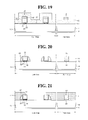
Referring to example FIG. 14, a spacer may be formed over either sidewall of the first polysilicon pattern 61, the second polysilicon pattern 62, and the third polysilicon pattern 63. An oxide layer, a nitride layer, and an oxide layer may be sequentially stacked over the semiconductor substrate 10, and a sixth etch process may be performed to form a sixth oxide layer pattern 29, a second nitride layer pattern 45, and a seventh oxide layer pattern 30, to thereby form the spacer.
Since the first polysilicon pattern 61 and the second polysilicon pattern 62 contact each other, with the fourth oxide layer pattern 28 interposed therebetween, the spacer may be formed over the sidewall of the second polysilicon pattern 62 with which the first polysilicon pattern 61 does not contact. Although the spacer has an oxide-nitride-oxide (ONO) structure in embodiments, the present disclosure is not limited thereto. For example, the spacer may have an oxide-nitride (ON) structure.
Referring to example FIG. 15, a fifth ion implantation process may be performed on the semiconductor substrate 10 to form a fifth impurity area 17 (S14 through S19). The fifth impurity area 17 may be a drain area in the cell area and a source or drain area in the peripheral area. The fifth ion implantation process may be performed using a variety of masks. This is done because n-type impurity ions or p-type impurity ions are selectively implanted according to gates. Thus, the proper ions may be implanted into each of gates using the masks.
A silicide layer 70 may be formed over each of exposed portions of the first polysilicon pattern 61, the second polysilicon pattern 62, the third polysilicon pattern 63, the third impurity area 15, and the fifth impurity area 17 (S20). A silicide process may be performed over the semiconductor substrate 10 using materials such as titanium (Ti), cobalt (Co), and nickel (Ni) to form the silicide layer 70. The silicide layer 70 may be formed in an area in which a contact is to be formed later.
Referring to example FIG. 16, an interlayer dielectric 80 may be formed over the semiconductor substrate 10, and contacts 85 may be formed in the interlayer dielectric 80 (S21). The contact 80 connected to the first polysilicon pattern 61 and the second polysilicon pattern 62 may be formed in one body such that the contact 80 is simultaneously connected to the first polysilicon pattern 61 and the second polysilicon pattern 62.
A nitride layer may be additionally formed over the semiconductor substrate 10, and then, the interlayer dielectric 80 may be formed. Also, an interconnection forming process may be performed over the interlayer dielectric 80 including the contacts.
Example FIGS. 15 to 21 are plane views and sectional views of a flash memory device according to embodiments. Table 2 below shows photo steps illustrating a process sequence of a flash memory device according to embodiments.
TABLE 2
Cell area
Logic area Photo step # (HV-MV Full share)
AA(DUV/OPC/PSM) S1 AA(DUV/OPC/PSM)
S2 DNW
PWA S3 PWA
PWB S4 PWB(Share with HV)
NWA S5 NWA
NWB S6 PWB(Share with HV)
S7 ONO and 1st poly dep
S8 Memory Gate
LA(gate oxide) S9 LA(gate oxide)
Poly etch-back
S10 Spacer Poly etch
GC(DUV/OPC/PSM) S11 GC(DUV/OPC/PSM)
S12 Cell Source IMP
LN S13 LN
LNH S14 LNH(Share with HV)
LP S15 LP
LPH S16 LPH(Share with HV)
XP S17 XP
XN S18 XN
NSAL S19 NSAL
Cont~M3 + Passivation S20~S26 Cont~M3 + Passivation
21 Mask TOTAL 26 Mask
Referring to example FIG. 17, a device isolation layer may be formed on a semiconductor substrate 10 including a cell area and a peripheral area to define an active area (S1). A first ion implantation process may be performed on the semiconductor substrate 10 to form a first impurity area 12 in the cell area and a second impurity area 14 in the peripheral area (S2 through S6).
Here, the first ion implantation process may be performed using a variety of masks. This may be done because ion implantation concentrations and kinds of ions are different according to voltage levels used in the gates. Thus, the proper ions and concentrations may be implanted into each of the gates using the masks. The first impurity area 12 and the second impurity area 14 may be wells, respectively.
When the first ion implantation process is performed, a well in which a high voltage gate is to be formed may be formed at the same time. Also, when the first ion implantation process for forming the first impurity area 12 and the second impurity area 14 is performed, an ion implantation process for adjusting a threshold voltage of a memory gate may be additionally performed. Here, since a mask used for forming the first impurity area 12 and the second impurity area 14 may be simultaneously used in the ion implantation process for the adjusting the threshold voltage, the number of masks may be reduced.
Referring to example FIG. 18, an oxide-nitride-oxide layer including a first oxide layer 21, a first nitride layer 41, and a second oxide layer 22, a first polysilicon layer 51, and a hard mask layer 46 may be formed over the semiconductor substrate 10 including the first impurity area 12 and the second impurity area 14 (S7). A fifth photoresist pattern 5 may be formed over the hard mask layer 46. The first oxide layer 21, the first nitride layer 41, the second oxide layer 22, the first polysilicon layer 51, and the hard mask layer 46 may be formed over all of the cell and peripheral areas.
Referring to example FIG. 9, a seventh etch process may be performed using fifth photoresist pattern 5 as a mask to form a first oxide layer pattern 25, a first nitride layer pattern 43, a second oxide layer pattern 26, a first polysilicon pattern 61, and a hard mask pattern 47 over only the cell area of the semiconductor substrate 10 (S8). Here, the first oxide layer 21, the first nitride layer 41, the second oxide layer 22, the first polysilicon layer 51, and the hard mask layer 46, which may be formed in the peripheral area, may be completely removed by the seventh etch process.
A fourth oxide layer 27 and a second polysilicon layer 52 are formed in the cell area including the first oxide layer pattern 25, the first nitride layer pattern 43, the second oxide layer pattern 26, the first polysilicon pattern 61, and the hard mask pattern 47 and the peripheral area of the semiconductor substrate 10.
Referring to example FIG. 20, a fourth oxide layer pattern 28 and a second polysilicon pattern 62 may be formed over sidewalls of the first polysilicon pattern 61 formed in the cell area, and the fourth oxide layer pattern 28 and third polysilicon pattern 63 may be formed in the peripheral area (S9 and S10). Here, a sixth photoresist pattern 6 may be formed over the second polysilicon layer 52 of the peripheral area, and an eighth etch process may be performed on the semiconductor substrate 10 to form the fourth oxide layer pattern 28, the second polysilicon pattern 62, and the third polysilicon pattern 63. When the eighth etch process is performed, the hard mask pattern 47 may be removed at the same time.
Referring to example FIG. 21, a fourth photoresist pattern 4 may be formed over the semiconductor substrate 10, and the fourth oxide layer pattern 28 and the second polysilicon pattern 62 disposed between the first polysilicon patterns 61 adjacent to each other in the cell area may be removed. Here, the fourth photoresist pattern 4 opens only an area, in which a common source line is to be formed, between the first polysilicon patterns 61 adjacent to each other, to remove the fourth oxide layer pattern 28 and the second polysilicon pattern 62 formed between the first polysilicon patterns 61 adjacent to each other. Thus, the fourth oxide layer pattern 28 and the second polysilicon pattern 62 may be formed over only one sidewall of the sidewalls of the first oxide layer pattern 25, the first oxide layer pattern 43, the second oxide layer pattern 26, and the first polysilicon pattern 61. The second polysilicon pattern 62 formed over the one sidewall of the first polysilicon pattern 61 may be a select gate.
The following processes may be performed using the same process as example FIG. 12 below of the previously described embodiments. That is, in the method of manufacturing the flash memory device according to embodiments, when the walls of the cell area and the peripheral area are formed, the ion implantation process for adjusting the threshold voltage may be performed at the same time to simplify the photomasking process.
Also, when the ONO layer below the memory gate is formed, the ONO layer formed in the peripheral area is not removed. That is, the ONO layer formed in the peripheral area may be removed at the same time when the etch process for forming the polysilicon pattern that may be the memory gates is performed. Therefore, the number of masks may be reduced.
Table 3 below shows operation conditions of the memory device according to the embodiments.
TABLE 3
PROGRAM ERASE READ
Method Channel Hot BTBT Induced Reverse
Electron Hot Hole
Oper. Mode Bit Sector Random
Access
Selected W/L +HV_P1 −HV_E1 Vcc
S/L +HV_P2 +HV_E2 0 V
B/L Back bias Floating Vd_read
Bulk 0 V 0 V 0 V
Un- Same W/L W/L +HV_P1 −HV_E1 Vcc
selected
S/L +HV_P2 Floating 0 V
B/L Floating Floating 0 V
Bulk 0 V 0 V 0 V
Same B/L W/L 0 V 0 V 0 V
S/L +HV_P2 0 V 0 V
B/L Back bias Floating Vd_read
Bulk 0 V 0 V 0 V
As shown in Table 3, the program operation may be implemented by the Channel Hot Electron (CHE) method, and the erase operation may be implemented by the band-to-band-tunneling (BTBT) induced hot hole method. Also, the read operation may be implemented by a reverse method.
In the operation mode, the program operation may be executed by a bit unit, the erase operation may be executed by a sector unit, and the read operation may be provided in the random access mode. Among the items listed in Table 3, the back bias voltage may be applied to control current.
It will be obvious and apparent to those skilled in the art that various modifications and variations can be made in the embodiments disclosed. Thus, it is intended that the disclosed embodiments cover the obvious and apparent modifications and variations, provided that they are within the scope of the appended claims and their equivalents.

Claims (16)

1. A method comprising:
preparing a semiconductor substrate including a cell area and a peripheral area;
forming a device isolation layer in the semiconductor substrate;
forming a first well in the cell area of the semiconductor substrate and forming an oxide-nitride-oxide layer over the cell area of the semiconductor substrate having the device isolation layer;
forming a second well in the peripheral area of the semiconductor substrate and forming a first oxide layer over the peripheral area of the semiconductor substrate;
forming a first polysilicon layer over the oxide-nitride-oxide layer and the first oxide layer and performing a first etch process to form a memory gate including an oxide-nitride-oxide layer pattern and a first polysilicon pattern in the cell area;
forming a second oxide layer pattern and a second polysilicon pattern over a first sidewall of the memory gate and forming a gate in the peripheral area;
performing a third etch process on the semiconductor substrate so that the second oxide layer pattern and the second polysilicon pattern remain over only the first sidewall of the memory gate to form a select gate; and
forming a first impurity area being a source area in the semiconductor substrate between the memory gates adjacent to each other using a photoresist pattern used in the third etch process.
2. The method of claim 1, wherein, when the first etch process is performed, the first oxide layer remains over the semiconductor substrate including the peripheral area.
3. The method of claim 2, wherein, when the first etch process is performed, the first polysilicon layer remains over the semiconductor substrate including the peripheral area.
4. The method of claim 3, wherein the gate formed in the peripheral area is formed by performing a second etch process over the first oxide layer and the first polysilicon layer.
5. The method of claim 4, wherein the gate formed in the peripheral area includes a third oxide layer pattern and a third polysilicon pattern.
6. The method of claim 1, wherein the performing of the third etch process includes removing the second oxide layer pattern and the second polysilicon pattern formed between the memory gates adjacent to each other so that the second oxide layer pattern and the second polysilicon pattern remain over only the first sidewall of the memory gate.
7. The method of claim 1, further including performing an ion implantation process on an entire surface of the semiconductor substrate including the first impurity area to form a second impurity area on the semiconductor substrate including the second oxide layer pattern and the second polysilicon pattern of the memory gate and the gate in the peripheral area.
8. The method of claim 1, further including forming spacers over the sidewall of the memory gate and a sidewall of the gate in the peripheral area.
9. The method of claim 8, further including forming an interlayer dielectric over the semiconductor substrate including the spacers.
10. The method of claim 9, including forming contacts in the interlayer dielectric.
11. The method of claim 9, wherein the contact connected to the memory gate is simultaneously connected to the first polysilicon pattern and the second polysilicon pattern.
12. A method comprising:
preparing a semiconductor substrate including a cell area and a peripheral area;
forming a device isolation layer in the semiconductor substrate;
forming a first well in the cell area of the semiconductor substrate and a second well in the peripheral area;
forming a memory gate comprising an oxide-nitride-oxide layer pattern and a first polysilicon pattern over the cell area of the semiconductor substrate;
forming a first oxide layer and a second polysilicon layer over the semiconductor substrate including the memory gate;
forming a second oxide layer pattern and a second polysilicon pattern over a first sidewall of the memory gate, and simultaneously, forming a gate in the peripheral area;
performing a first etch process on the semiconductor substrate so that the second oxide layer pattern and the second polysilicon pattern remain over only the first sidewall of the memory gate to form a select gate; and
forming a first impurity area being a source area in the semiconductor substrate between the memory gates adjacent to each other,
wherein the forming of the memory gate including the oxide-nitride-oxide layer pattern and the first polysilicon pattern over the semiconductor substrate including the cell area includes:
forming an oxide-nitride-oxide layer over the semiconductor substrate including the cell area and the peripheral area;
forming a first polysilicon layer over the semiconductor substrate including the cell area and the peripheral area; and
performing a second etch process on the oxide-nitride-oxide layer and the first polysilicon layer to form the memory gate including the oxide-nitride-oxide layer pattern and the first polysilicon pattern, and
wherein, when the second etch process for forming the memory gate is performed, the oxide-nitride-oxide layer and the first polysilicon layer formed in the peripheral area are completely removed.
13. The method of claim 12, wherein the gate formed in the peripheral area is formed by performing a third etch process on the first oxide layer and the second polysilicon layer.
14. The method of claim 12, wherein the performing of the first etch process includes removing the second oxide layer pattern and the second polysilicon pattern formed between the memory gates adjacent to each other so that the second oxide layer pattern and the second polysilicon pattern remain over only the first sidewall of the memory gate.
15. The method of claim 12, further including performing an ion implantation process on an entire surface of the semiconductor substrate comprising the first impurity area to form a second impurity area over the semiconductor substrate including the second oxide layer pattern and the second polysilicon pattern of the memory gate and the gate of the semiconductor substrate.
16. The method of claim 12, further including forming spacers over a sidewall of the memory gate and a sidewall of the gate in the peripheral area.
US12/544,761 2008-12-24 2009-08-20 Method of manufacturing flash memory device Expired - Fee Related US7888211B2 (en)

Applications Claiming Priority (2)

Application Number Priority Date Filing Date Title
KR10-2008-0133681 2008-12-24
KR1020080133681A KR100936627B1 (en) 2008-12-24 2008-12-24 Flash memory device and method for manufacturing the same

Publications (2)

Publication Number Publication Date
US20100159660A1 US20100159660A1 (en) 2010-06-24
US7888211B2 true US7888211B2 (en) 2011-02-15

Family

ID=41809740

Family Applications (1)

Application Number Title Priority Date Filing Date
US12/544,761 Expired - Fee Related US7888211B2 (en) 2008-12-24 2009-08-20 Method of manufacturing flash memory device

Country Status (5)

Country Link
US (1) US7888211B2 (en)
JP (1) JP2010153780A (en)
KR (1) KR100936627B1 (en)
CN (1) CN101764097A (en)
TW (1) TW201025511A (en)

Cited By (2)

* Cited by examiner, † Cited by third party
Publication number Priority date Publication date Assignee Title
US9029931B2 (en) 2010-09-22 2015-05-12 Renesas Electronics Corporation Semiconductor device and manufacturing method thereof
US9960176B2 (en) 2015-11-05 2018-05-01 Taiwan Semiconductor Manufacturing Co., Ltd. Nitride-free spacer or oxide spacer for embedded flash memory

Families Citing this family (8)

* Cited by examiner, † Cited by third party
Publication number Priority date Publication date Assignee Title
CN102339833B (en) * 2010-07-21 2013-04-24 中国科学院微电子研究所 High-reliability split-gate nonvolatile memory structure with high-speed low-voltage operation function
US20140167142A1 (en) * 2012-12-14 2014-06-19 Spansion Llc Use Disposable Gate Cap to Form Transistors, and Split Gate Charge Trapping Memory Cells
KR20140121614A (en) 2013-04-08 2014-10-16 에스케이하이닉스 주식회사 Nonvolatile memory device
US9466496B2 (en) * 2013-10-11 2016-10-11 Cypress Semiconductor Corporation Spacer formation with straight sidewall
CN104576522B (en) * 2013-10-16 2017-10-24 上海华虹宏力半导体制造有限公司 The integrated approach of surface channel CMOS logic device and SONOS devices
JP5956093B1 (en) * 2014-10-15 2016-07-20 株式会社フローディア Semiconductor device and manufacturing method thereof
CN104538361B (en) * 2014-12-25 2017-08-25 上海华虹宏力半导体制造有限公司 The method for controlling flash cell threshold voltage
CN106816368B (en) * 2015-12-01 2019-11-05 中芯国际集成电路制造(上海)有限公司 The forming method of semiconductor structure and CMOS transistor

Citations (2)

* Cited by examiner, † Cited by third party
Publication number Priority date Publication date Assignee Title
KR20060103153A (en) 2005-03-23 2006-09-28 가부시끼가이샤 르네사스 테크놀로지 Semiconductor memory device and manufacturing method thereof
US7300833B2 (en) * 2001-03-12 2007-11-27 Renesas Technology Corp. Process for producing semiconductor integrated circuit device

Family Cites Families (3)

* Cited by examiner, † Cited by third party
Publication number Priority date Publication date Assignee Title
JP4718104B2 (en) * 2003-02-17 2011-07-06 ルネサスエレクトロニクス株式会社 Semiconductor device
US20070021960A1 (en) * 2005-07-20 2007-01-25 Mclean Marc System and method for communicating with a network
JP2008166325A (en) * 2006-12-27 2008-07-17 Renesas Technology Corp Method of manufacturing semiconductor device

Patent Citations (3)

* Cited by examiner, † Cited by third party
Publication number Priority date Publication date Assignee Title
US7300833B2 (en) * 2001-03-12 2007-11-27 Renesas Technology Corp. Process for producing semiconductor integrated circuit device
KR20060103153A (en) 2005-03-23 2006-09-28 가부시끼가이샤 르네사스 테크놀로지 Semiconductor memory device and manufacturing method thereof
US20070221960A1 (en) * 2005-03-23 2007-09-27 Motoi Ashida Semiconductor memory device and manufacturing method thereof

Cited By (7)

* Cited by examiner, † Cited by third party
Publication number Priority date Publication date Assignee Title
US9029931B2 (en) 2010-09-22 2015-05-12 Renesas Electronics Corporation Semiconductor device and manufacturing method thereof
US9231115B2 (en) 2010-09-22 2016-01-05 Renesas Electronics Corporation Semiconductor device and manufacturing method thereof
US9960176B2 (en) 2015-11-05 2018-05-01 Taiwan Semiconductor Manufacturing Co., Ltd. Nitride-free spacer or oxide spacer for embedded flash memory
US10347649B2 (en) 2015-11-05 2019-07-09 Taiwan Semiconductor Manufacturing Co., Ltd. Nitride-free spacer or oxide spacer for embedded flash memory
US10475805B2 (en) 2015-11-05 2019-11-12 Taiwan Semiconductor Manufacturing Co., Ltd. Nitride-free spacer or oxide spacer for embedded flash memory
US10847530B2 (en) 2015-11-05 2020-11-24 Taiwan Semiconductor Manufacturing Co., Ltd. Nitride-free spacer or oxide spacer for embedded flash memory
US11264400B2 (en) 2015-11-05 2022-03-01 Taiwan Semiconductor Manufacturing Company, Ltd. Nitride-free spacer or oxide spacer for embedded flash memory

Also Published As

Publication number Publication date
JP2010153780A (en) 2010-07-08
CN101764097A (en) 2010-06-30
KR100936627B1 (en) 2010-01-13
TW201025511A (en) 2010-07-01
US20100159660A1 (en) 2010-06-24

Similar Documents

Publication Publication Date Title
US7888211B2 (en) Method of manufacturing flash memory device
US8044451B2 (en) Method of manufacturing semiconductor device having notched gate MOSFET
US6204126B1 (en) Method to fabricate a new structure with multi-self-aligned for split-gate flash
US20150140766A1 (en) Method of forming and structure of a non-volatile memory cell
US7029976B1 (en) Method for SONOS EFLASH integrated circuit
JP2004282083A (en) Flash memory comprising local sonos structure utilizing notch gate, and manufacturing method thereof
US8110461B2 (en) Flash memory device and manufacturing method of the same
US7553725B2 (en) Nonvolatile memory devices and methods of fabricating the same
US6787419B2 (en) Method of forming an embedded memory including forming three silicon or polysilicon layers
US7348241B2 (en) Cell structure of EPROM device and method for fabricating the same
US20100165736A1 (en) Flash memory device and manufacturing method of the same
US20050173753A1 (en) Semiconductor device and method of fabricating the same
JP4030839B2 (en) Manufacturing method of memory integrated circuit device
US7948022B2 (en) Flash memory device and method for manufacturing the same
JP2007067027A (en) Manufacturing method of built-in non-volatile memory
KR100464443B1 (en) Cell structure of EPROM device and fabrication thereof
US7875924B2 (en) Flash memory device and method for fabricating the same
JP2002208645A (en) Non-volatile semiconductor storage and manufacturing method therefor
KR20050069114A (en) Memory device with one poly split gate structure and fabricating method thereof
US20070077707A1 (en) Non volatile memory device and method of manufacturing the same
KR100594325B1 (en) Method of manufacturing semiconductor device having notched gate mosfet
KR100932135B1 (en) Flash memory device manufacturing method
US9048263B2 (en) Manufacturing method of non-volatile memory
JP2005197726A (en) Method for manufacturing non-volatile memory device
KR101033402B1 (en) Flash memory device and manufacturing method the same

Legal Events

Date Code Title Description
AS Assignment

Owner name: DONGBU HITEK CO., LTD.,KOREA, REPUBLIC OF

Free format text: ASSIGNMENT OF ASSIGNORS INTEREST;ASSIGNOR:SHIM, CHEON-MAN;REEL/FRAME:023125/0763

Effective date: 20090803

Owner name: DONGBU HITEK CO., LTD., KOREA, REPUBLIC OF

Free format text: ASSIGNMENT OF ASSIGNORS INTEREST;ASSIGNOR:SHIM, CHEON-MAN;REEL/FRAME:023125/0763

Effective date: 20090803

FEPP Fee payment procedure

Free format text: PAYOR NUMBER ASSIGNED (ORIGINAL EVENT CODE: ASPN); ENTITY STATUS OF PATENT OWNER: LARGE ENTITY

FPAY Fee payment

Year of fee payment: 4

AS Assignment

Owner name: DB HITEK CO., LTD., KOREA, REPUBLIC OF

Free format text: CHANGE OF NAME;ASSIGNOR:DONGBU HITEK CO., LTD.;REEL/FRAME:044559/0819

Effective date: 20171101

FEPP Fee payment procedure

Free format text: MAINTENANCE FEE REMINDER MAILED (ORIGINAL EVENT CODE: REM.); ENTITY STATUS OF PATENT OWNER: LARGE ENTITY

LAPS Lapse for failure to pay maintenance fees

Free format text: PATENT EXPIRED FOR FAILURE TO PAY MAINTENANCE FEES (ORIGINAL EVENT CODE: EXP.); ENTITY STATUS OF PATENT OWNER: LARGE ENTITY

STCH Information on status: patent discontinuation

Free format text: PATENT EXPIRED DUE TO NONPAYMENT OF MAINTENANCE FEES UNDER 37 CFR 1.362

FP Lapsed due to failure to pay maintenance fee

Effective date: 20190215