US7848404B2 - Current mode logic multi-tap feed-forward equalizer - Google Patents
Current mode logic multi-tap feed-forward equalizer Download PDFInfo
- Publication number
- US7848404B2 US7848404B2 US11/732,908 US73290807A US7848404B2 US 7848404 B2 US7848404 B2 US 7848404B2 US 73290807 A US73290807 A US 73290807A US 7848404 B2 US7848404 B2 US 7848404B2
- Authority
- US
- United States
- Prior art keywords
- differential
- signals
- future
- past
- present
- Prior art date
- Legal status (The legal status is an assumption and is not a legal conclusion. Google has not performed a legal analysis and makes no representation as to the accuracy of the status listed.)
- Active, expires
Links
Images


Classifications
-
- H—ELECTRICITY
- H04—ELECTRIC COMMUNICATION TECHNIQUE
- H04L—TRANSMISSION OF DIGITAL INFORMATION, e.g. TELEGRAPHIC COMMUNICATION
- H04L25/00—Baseband systems
- H04L25/02—Details ; arrangements for supplying electrical power along data transmission lines
- H04L25/03—Shaping networks in transmitter or receiver, e.g. adaptive shaping networks
- H04L25/03006—Arrangements for removing intersymbol interference
- H04L25/03343—Arrangements at the transmitter end
-
- H—ELECTRICITY
- H04—ELECTRIC COMMUNICATION TECHNIQUE
- H04L—TRANSMISSION OF DIGITAL INFORMATION, e.g. TELEGRAPHIC COMMUNICATION
- H04L25/00—Baseband systems
- H04L25/02—Details ; arrangements for supplying electrical power along data transmission lines
- H04L25/0264—Arrangements for coupling to transmission lines
- H04L25/028—Arrangements specific to the transmitter end
Definitions
- This invention generally relates to physical layer (PHY) communication circuitry and, more particularly, to a system and method for using a current mode logic (CML) summing amplifier with multiple taps as feed-forward equalizer (FFE) in high speed data transmission to compensate for losses in the transmission medium.
- CML current mode logic
- FFE feed-forward equalizer
- FIG. 1 is a diagram illustrating a high speed data transmission system (prior art).
- the data channel may be a printed circuit board (PCB) trace and include connectors and vias on the PCB board, or a length of transmission line to connect a receiver.
- Significant inter-symbol interference (ISI) may occur that degrades the received signal and causes errors, in the receiving data due to the dispersive behavior the channel from skin effect of metal, dielectric loss, cross-talk, and reflection due to impedance mismatches.
- a feed forward equalizer (FFE) and/or a decision feed-back equalizer (DFE) may be used for mitigating the problem.
- a feed-forward equalizer is often used in a transmitter.
- FIG. 2 depicts a transversal filter FFE equalizer (prior art).
- the FFE consists of multiple distributed gain stages with the same number of delay taps.
- the delay is normally a fractional of the bit period and may be realized with either passive or active elements.
- this type of FFE circuitry has the disadvantage of consuming power. It is difficult to control the delay elements, especially when more stage/taps are needed to compensate multiple post-cursor ISI. Another disadvantage is that this type of FFE cannot compensate for pre-cursor ISI.
- FIG. 3 is block diagram depicting a FFE with a half-symbol spaced finite impulse response (FIR) (prior art).
- the input of the data stream is supplied to an 8-stage shift register, which forms the tapped delay line of the FIR filter.
- the shift register operates at a full-rate clock and consists of transparent latches with even and odd stages using opposite clock polarity, so each stage creates a delay of a half clock period.
- the eight delayed copies of the input are then multiplied by eight FIR filter coefficients and summed together as follows. First, digital signals from individual taps are supplied to exclusive-or (XOR) gates along with the respective polarity bits of the tap coefficients P 0 -P 7 .
- XOR exclusive-or
- the polarity-adjusted digital signals then drive individual buffer stages with programmable tail currents. These stages generate differential output currents, each being a product of the tail current (representing the magnitude of the tap coefficient) and a polarity-adjusted delayed copy of the input data. This operation generates FIR filter partial sums. Finally, the differential currents from individual stages are summed together at a common differential resistive load, providing the final output of the FIR filter.
- This FFE configuration uses latching circuitry to create half-symbol spaced delays, and even more stages are needed for more dispersive channels. XOR gates in the high speed signal path degrade the signal and add jitter to the data. Also, simple coefficient control differential circuits may not provide the right signal level and shape for optimal performance.
- an FFE could operate with full rate and symbol-spaced delay, using control coefficients to shape signals with swing and slew, and provide optimal equalization performance, to compensate for pre-cursor and post-cursor inter-symbol interference in high dispersive channels.
- a method for feed-forward equalization in a transmission system.
- the method accepts a serial stream of input digital data signals. For each input data signal, a temporal sequence of signals is generated. Each of the signals in the temporal sequence is selectively shaped. Shaping may include varying the degree of amplification, modifying the slew rate, or varying the time delay. The contributions of the selectively shaped signals in the temporal sequence are then selectively weighted, and a summed output signal is transmitted.
- each input signal can be used to generate a sequence of past, present, and future representations of the signal.
- accepting the serial stream of input data signals may entail accepting the serial stream of input data signals at a clock rate
- generating the temporal sequence of signals may includes the substeps of: gating input data signals through a first register at the clock rate to supply future signals; gating future signal through a second register at the clock rate to supply present signals; and, gating present signal through a third register at the clock rate to supply past signals.
- the method may be enabled using differential signals, so the weighting the contributions of the past, present, future signals includes establishing a 3-tap differential summing amplifier with a common differential output and parallel differential present, past, and future taps.
- Each of the differential taps is enabled in response to accepting a corresponding selectively shaped past, present, and future signal.
- Each of the differential taps is weighted in response to using a corresponding past, present, and future weighting signal to control current flow through the tap.
- FIG. 1 is a diagram illustrating a high speed data transmission system (prior art).
- FIG. 2 depicts a transversal filter FFE equalizer (prior art).
- FIG. 3 is block diagram depicting a FFE with a half-symbol spaced finite impulse response (FIR) (prior art).
- FIR finite impulse response
- FIG. 4 is a schematic block diagram of a transmitter with a system for feed-forward equalization.
- FIG. 5 is a diagram depicting a temporal sequence of signals associated with three consecutively received input data signals.
- FIG. 6 is a schematic diagram depicting a fundamental representation of the summing amplifier of FIG. 4 .
- FIG. 7 is a schematic block diagram depicting a more detailed example of the feed-forward equalizer of FIG. 4 .
- FIG. 8 is a schematic diagram depicting a 3-tap example of a differential signal summing amplifier.
- FIG. 9 is a schematic drawing depicting a more detailed example of the pre-driver module of FIG. 7 .
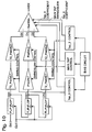
- FIG. 10 is a schematic block diagram depicting another variation of the FFE of FIG. 4 .
- FIG. 11 is a schematic drawing depicting another variation of the summing amplifier.
- FIG. 12 is a flowchart illustrating a method for feed-forward equalization in a data transmission system.
- FIG. 4 is a schematic block diagram of a transmitter 300 with a system for feed-forward equalization.
- the system 302 comprises a temporal circuit 304 having an input on line 306 to accept a serial stream of input digital data signals, and outputs on line 308 to supply a temporal sequence of signals for each input data signal.
- n represents the number of signals in a temporal sequence.
- FIG. 5 is a diagram depicting a temporal sequence of signals associated with three consecutively received input data signals.
- a temporal sequence of signals is a presentation of an input signal with multiple delayed representations.
- an input digital “1” value can be represented as a series of “1” values, where each “1” value is delayed from the next by one clock cycle.
- the temporal series is shown as consisting of 5 values in this example, the invention is not limited to any particular value.
- each of the three consecutive input data signals is shown as a “1” value.
- a pre-driver module 310 has inputs on line 308 to accept the temporal sequence of signals and outputs on line 312 to supply selectively shaped signals in the temporal sequence.
- the pre-driver module 310 permits the first value, for example, in a temporal series to be shaped differently from the second value.
- Selectively shaping signals in the temporal sequence may involve adjusting the level of amplifying, controlling delay, or modifying slew rate. However, the adjustment of one shaping feature may also result in modifications to the other features. Since n signals are received on lines 308 a through 308 n, n signals are supplied on lines 312 a through 312 n . In, one aspect, the signals are shaped in response to bias signals received on line 320 . Since there are n signals to shape, there are n bias signals on lines 320 a through 320 n.
- a summing amplifier 314 has inputs on line 312 to accept the selectively shaped signals in the temporal sequence.
- the summing amplifier selectively weights the contributions of the shaped signals in response to weighting signals received on line 316 , and transmits a summed output signal on line 318 . Since there are n shaped signals, there are n weighting signals on lines 316 a through 316 n .
- the summed output signal may be transmitted via a connector medium, for example, or as another example, transmitted via conductive traces to a different region of the same printed circuit board (PCB).
- FIG. 6 is a schematic diagram depicting a fundamental representation of the summing amplifier of FIG. 4 .
- the summing amplifier 314 includes a resistor 500 with a first end 502 connected to a first voltage source (Vdd), and a common output on line 320 connected to, a second end of the resistor 504 .
- Each tap 506 a through 506 n is connected in common to the second end 504 of the resistor and weighted in response to accepting a corresponding weighting signal on lines 316 a through 316 n , to control current flow through the tap.
- each tap is represented by a FET is series with a current source.
- the shaped signal on line 312 a enables FET 508 a and current (weighting) through the tap is controlled using the weighting signal on line 316 a .
- Other ways of enabling taps with the same functionality as described above would be known by those with skill in the art.
- the invention is not limited to just this example of a single-ended signal summing amplifier.
- FIG. 7 is a schematic block diagram depicting a more detailed example of the feed-forward equalizer of FIG. 4 .
- the temporal circuit 304 includes an input on line 600 to accept a clock having a clock rate.
- a future register 602 has an input on line 306 to accept the serial stream of input data signals, and on input on line 600 accepts the clock.
- the future register 602 gates the input data signals at the clock rate to supply future signals on line 308 a.
- a present register 604 has an input on line 308 a to accept the future signals, and an input on line 600 to accept the clock.
- the present register 604 gates the future signals at the clock rate to supply the present signals on line 308 b .
- a past register 606 has an input on line 308 b to accept the present signals, and an input on line 600 to accept the clock.
- the past register 606 gates the present signals at the clock rate to supply the past signals on line 308 c.
- a bias circuit 608 has outputs on lines 320 a , 320 b , and 320 c to supply past, present, and future bias signals, respectively.
- the pre-driver module 310 includes a future pre-driver 610 to accept future signals on line 308 a and the future bias signal on line 320 a .
- the future pre-driver 610 supplies selectively shaped future signals on line 312 a in response to the future bias signal.
- a present pre-driver 612 accepts present signals on line 308 b and the present bias signal on line 320 b .
- the present pre-driver 612 supplies selectively shaped present signals on line 312 b in response to the present bias signal.
- a past pre-driver 614 accepts past signals on line 308 c and the past bias signal on line 320 c .
- the past pre-driver 614 supplies selectively shaped past signals on line 312 c in response to the past bias signal.
- the summing amplifier 314 has inputs on lines 312 a , 312 b , and 312 c to accept the past, present, and future bias signals, respectively.
- the summing amplifier 314 selectively weights the selectively shaped future signals in response to the future weighting signal on line 316 a .
- the selectively shaped present signals are weighted in response to the present weighting signal on line 316 b
- the selectively shaped past signal is weighed in response to the past weighting signal on 316 c.
- FIG. 8 is a schematic diagram depicting a 3-tap example of a differential signal summing amplifier.
- the temporal circuit accepts a serial stream of differential input data signals and supplies differential past, present, and future signals.
- the pre-driver module supplies differentially shaped past, present, and future signals, and the summing amplifier transmits a summed differential output signal.
- One version of a differential summing amplifier includes a differential pair of resistors 700 and 702 with first ends 704 and 706 , respectively, connected to a first voltage source (Vdd).
- a common differential output 320 a and 320 b is connected to a second end 708 and 710 of resistor 700 and 702 , respectively.
- the taps are shown enabled a differential amplifiers and controllable current sources.
- the future tap 712 a includes a pair of differential transistors 714 and 716 having gates to accept the selectively shaped differential future signals 312 a 1 and 312 a 2 , respectively.
- Transistors 714 and 716 have sources, and they have drains connected to the second ends 708 and 710 of the resistor 700 and 702 , respectively.
- a future current bias circuit 718 has an input on line 316 a to accept the future weighting signal, an input connected to the sources of the pair of differential transistors 714 / 716 , and an output connected to the second voltage source (e.g., ground) on line 720 .
- the second voltage source e.g., ground
- the present tap 712 b includes a pair of differential transistors 722 and 724 having gates to accept the selectively shaped differential present signals 312 b 1 and 312 b 2 , respectively.
- the transistors 722 / 724 have sources, and they have drains connected to the second ends 708 and 710 of the resistor 700 and 702 , respectively.
- a present current bias circuit 726 has an input on line 316 b to accept the present weighting signal, an input connected to the sources of the pair of differential transistors 722 / 724 , and an output connected to the second voltage source (e.g., ground) on line 728 .
- the past tap 712 c includes a pair of differential transistors 730 and 732 having gates to accept the selectively shaped differential past signals 312 c 1 and 312 c 2 , respectively.
- the transistors 730 / 732 have sources, and they have drains connected to the second ends 708 and 710 of the resistor 700 and 702 , respectively.
- a past current bias circuit 734 has an input on line 316 c to accept the past weighting signal, an input connected to the sources of the pair of differential transistors 730 / 732 , and an output connected to the second voltage source (e.g., ground) on line 734 .
- FIG. 9 is a schematic drawing depicting a more detailed example of the pre-driver module 310 of FIG. 7 .
- the past pre-driver 614 includes a pair of differential transistors 800 and 802 having gates to accept differential past signals 308 c 1 and 308 c 2 , respectively.
- the transistors 800 / 802 have sources, and they have drains connected to the first voltage source (Vdd) through an interposing resistor pair 804 and 806 .
- a pre-driver past current bias circuit 808 has an input on line 320 c to accept the past bias signal, an input connected to the sources of the differential transistors 800 and 802 , and an output connected to the second voltage source (e.g., ground).
- the present pre-driver 612 includes a pair of differential transistors 810 and 812 having gates to accept differential present signals on line 308 b 1 and 308 b 2 , respectively.
- the transistors 810 / 812 have sources, and they have drains connected to the first voltage source through an interposing resistor pair 804 and 806 .
- a pre-driver present current bias circuit 808 has an input on line 320 b to accept the present bias signal, an input connected to the sources of the pair of differential transistors 810 and 812 , and an output connected to the second voltage source.
- the future pre-driver 610 includes a pair of differential transistors 820 and 822 having gates to accept differential future signals on lines 308 a 1 and 308 a 2 , respectively.
- the transistors 820 / 822 have, sources, and drains connected to the first voltage source through an interposing resistor pair 824 and 826 , respectively.
- a pre-driver future current bias circuit 828 has an input on line 320 a to accept the future bias signal, an input connected to the sources of the pair of differential transistors 820 / 822 , and an output connected to the second voltage source.
- each pre-driver circuit has been depicted with a single stage of amplification, it should be understood that a pre-driver may be enabled with multiple stages of amplifications. Different circuit designs with the same functionality could be designed with those with skill in the art.
- FIG. 10 is a schematic block diagram depicting another variation of the FFE of FIG. 4 .
- the FFE consists of 4 main blocks: (1) the bit delay circuit, which provides the past bits, present bits, and future bits using high speed shift registers (e.g., flip-flops); (2) the pre-drive stages to reshape the signal waveforms; (3) the summing amplifier or summing driver to process the different bit information with weighted coefficients; and (4) the bias and control circuits for setting the tap coefficients, and swing and slew control of the pre-drive stages and summer circuits.
- a 3-tap architecture is shown as an example.
- This circuit may be used to receive the 3 pairs of 10 gigabyte per second (Gbs) signals (past, present, future bits) from the shift register circuit. Then, the bits are amplified and reshaped through 3 amplifier paths to drive the summing amplifier to perform feed-forward equalization.
- the output of the summing may be used, for example, to drive a 100 Ohm differential transmission line.
- the bias circuit and tap control circuitry are used to control each of the tap coefficients and swing/slew.
- CML circuits can be used in the implementation of all the circuit clocks used with the flip-flops, pre-drivers, and the summing amplifiers. Inductor peaking may be used to extend the bandwidth and, therefore, enhance the performance, as well as reduce the power. CML circuits and inductive peaking are design techniques well understood by those with skill in the art.
- FIG. 11 is a schematic drawing depicting another variation of the summing amplifier. Specifically, a 3-tap CML summing amplifier is shown. 3 pairs of differential input signals (D0P/D0N, D1P/D1N, and D2P/D2N) are summed though the 3-differential amplifiers with common loading. Inductors may be used for performance enhancement. The two side pairs (Tap—0EP/Tap—0EN and Tap—2EP/Tap—2EN) may be used as cascade switches to enable a non-FFE mode of summing amplifier operation. The weighting of the 3-tap amplifier pairs is controlled by the tap-control circuitry and is modified to obtain the desired tap control coefficient, as well as the slew/swing requirements.
- FIG. 12 is a flowchart illustrating a method for feed-forward equalization in a data transmission system. Although the method is depicted as a sequence of numbered steps for clarity, the numbering does not necessarily dictate the order of the steps. It should be understood that some of these steps may be skipped, performed in parallel, or performed without the requirement of maintaining a strict order of sequence.
- the method starts at Step 1100 .
- Step 1102 accepts a serial stream of input digital data signals. For each input data signal, Step 1104 generates a temporal sequence of signals. Step 1106 selectively shapes each of the signals in the temporal sequence. For example, Step 1106 may include a process such as adjusting amplification, controlling delay, or modifying slew rate. Step 1108 selectively weights the contributions of the selectively shaped signals in the temporal sequence. Step 1110 transmits a summed output signal.
- selectively weighting the contributions of the shaped signals in the temporal sequence in Step 1108 includes substeps.
- Step 1108 a establishes a multi-tap summing amplifier with a common output and a parallel tap for each shaped signal in the temporal sequence.
- Step 1108 b enables each of the taps in response to accepting a corresponding shaped signal.
- Step 1108 c weights each of the taps in response to accepting a corresponding weighting signal, to control current flow through the tap.
- accepting the serial stream of input data signals in Step 1102 includes accepting the serial stream of input data signals at a clock rate.
- generating the temporal sequence of signals includes: gating input data signals through a first register at the clock rate to supply future signals; gating future signal through a second register at the clock rate to supply present signals; and, gating present signal through a third register at the clock rate to supply past signals.
- selectively shaping signals in the temporal sequence in Step 1106 includes: shaping future signals in response to a future bias signal; shaping present signals in response to a present bias signal; and, shaping past signals in response to a past bias signal.
- selectively weighting the contributions of the shaped signals in the temporal sequence includes: weighting future signals in response to the future weighting signal; weighting present signals in response to the present weighting signal; and, weighting past signals in response to the past weighting signal.
- accepting the serial stream of input data signals in Step 1102 includes accepting a serial stream of differential input data signals.
- generating the temporal sequence of past, present, and future signals in Step 1104 includes generating differential past, present, and future signals.
- selectively shaping each of the past, present, and future signals in Step 1106 includes differentially amplifying the past, present, and future signals.
- Selectively weighting the contributions of the past, present, and future signals in Step 1108 includes differentially weighting the contributions of the past, present, future signals, and Step 1110 transmits a summed differential output signal.
- differentially weighting the contributions of the past, present, future signals includes Step 1108 a establishing a 3-tap differential summing amplifier with a common differential output and parallel differential present, past, and future taps.
- Step 1108 b enables each of the differential taps in response to accepting a corresponding selectively shaped past, present, and future signal, and
- Step 1108 c weights each of the differential taps in response to using a corresponding past, present, and future weighting signal to control current flow through the tap.
Abstract
Description
Claims (6)
Priority Applications (1)
| Application Number | Priority Date | Filing Date | Title |
|---|---|---|---|
| US11/732,908 US7848404B2 (en) | 2007-04-05 | 2007-04-05 | Current mode logic multi-tap feed-forward equalizer |
Applications Claiming Priority (1)
| Application Number | Priority Date | Filing Date | Title |
|---|---|---|---|
| US11/732,908 US7848404B2 (en) | 2007-04-05 | 2007-04-05 | Current mode logic multi-tap feed-forward equalizer |
Publications (2)
| Publication Number | Publication Date |
|---|---|
| US20080247453A1 US20080247453A1 (en) | 2008-10-09 |
| US7848404B2 true US7848404B2 (en) | 2010-12-07 |
Family
ID=39826857
Family Applications (1)
| Application Number | Title | Priority Date | Filing Date |
|---|---|---|---|
| US11/732,908 Active 2029-09-29 US7848404B2 (en) | 2007-04-05 | 2007-04-05 | Current mode logic multi-tap feed-forward equalizer |
Country Status (1)
| Country | Link |
|---|---|
| US (1) | US7848404B2 (en) |
Cited By (4)
| Publication number | Priority date | Publication date | Assignee | Title |
|---|---|---|---|---|
| US20100020862A1 (en) * | 2008-07-25 | 2010-01-28 | Taiwan Semiconductor Manufacturing Co., Ltd. | Input control circuit for the summer of a decision feedback equalizer |
| US20130208779A1 (en) * | 2012-02-10 | 2013-08-15 | International Business Machines Corporation | Feed-forward equalizer architectures |
| US8935125B1 (en) * | 2011-02-25 | 2015-01-13 | Smsc Holdings S.A.R.L. | Internal cable calibration and compensation |
| US10712769B2 (en) | 2017-08-16 | 2020-07-14 | Oracle International Corporation | Method and apparatus for clock signal distribution |
Families Citing this family (7)
| Publication number | Priority date | Publication date | Assignee | Title |
|---|---|---|---|---|
| US7525382B2 (en) * | 2007-08-04 | 2009-04-28 | Applied Micro Circuits Corporation | Multi-level slew and swing control buffer |
| US8483577B2 (en) * | 2008-12-19 | 2013-07-09 | Cisco Technology, Inc. | Programmable signal emphasis for optical transmitters |
| US8533252B2 (en) * | 2009-04-10 | 2013-09-10 | Realtek Semiconductor Corp. | Broad-band active delay line |
| TWI478488B (en) * | 2009-12-24 | 2015-03-21 | Realtek Semiconductor Corp | Broad-band active delay line and thereof method |
| US8537949B1 (en) * | 2010-06-30 | 2013-09-17 | Netlogic Microsystems, Inc. | Systems, circuits and methods for filtering signals to compensate for channel effects |
| US9379743B2 (en) * | 2014-07-30 | 2016-06-28 | Intel Corporation | Method and apparatus for signal edge boosting |
| JP2022143656A (en) * | 2021-03-18 | 2022-10-03 | Necプラットフォームズ株式会社 | Pre-emphasis circuit, control method, and program |
Citations (4)
| Publication number | Priority date | Publication date | Assignee | Title |
|---|---|---|---|---|
| US4709278A (en) * | 1984-09-21 | 1987-11-24 | Willi Studer Ag | Method and apparatus for producing and selectively equalizing a temporal relationship between series of digital signals |
| US5719633A (en) * | 1994-12-20 | 1998-02-17 | Matsushita Electric Industrial Co., Ltd. | Video signal format conversion apparatus using simplified shifting and processing control |
| US20050190873A1 (en) * | 2000-09-01 | 2005-09-01 | Smith Stephen F. | Digital-data receiver synchronization method and apparatus |
| US7183842B1 (en) * | 2005-05-26 | 2007-02-27 | Yu Hei Sunny Wai | Optimum composite cascode amplifier |
-
2007
- 2007-04-05 US US11/732,908 patent/US7848404B2/en active Active
Patent Citations (4)
| Publication number | Priority date | Publication date | Assignee | Title |
|---|---|---|---|---|
| US4709278A (en) * | 1984-09-21 | 1987-11-24 | Willi Studer Ag | Method and apparatus for producing and selectively equalizing a temporal relationship between series of digital signals |
| US5719633A (en) * | 1994-12-20 | 1998-02-17 | Matsushita Electric Industrial Co., Ltd. | Video signal format conversion apparatus using simplified shifting and processing control |
| US20050190873A1 (en) * | 2000-09-01 | 2005-09-01 | Smith Stephen F. | Digital-data receiver synchronization method and apparatus |
| US7183842B1 (en) * | 2005-05-26 | 2007-02-27 | Yu Hei Sunny Wai | Optimum composite cascode amplifier |
Non-Patent Citations (3)
| Title |
|---|
| "10+ gb/s 90-nm CMOS serial link demo in CBGA package", Rylov, S.; Reynolds, S.; Storaska, D.; Floyd, B.; Kapur, M.; Zwick, T.; Gowda, S.; Sorna, M., Solid-State Circuits, IEEE Journal of vol. 40, Issue 9, Sep. 2005 pp. 1987-1991. |
| "A 2.5- to 3.5-Gb/s Adaptive FIR Equalizer with Continuous-Time Wide Bandwidth Delay Line in 0.25mm CMOS,", X. F. Lin, J. Liu, H. Lee, and H. Liu, IEEE Journal of Solid-State Circuits, vol. 41, pp. 1908-1918, Aug. 2006. |
| "A 7-tap transverse analog-FIR filter in 0.12 um CMOS for equalization of 10Gb/s fiber-optic data systems", Reynolds, S.; Pepeljugoski, P.; Schaub, J.; Tierno, J.; Beisser, D., IEEE Solid-State Circuits Conference, 2005. Digest of Technical Papers. ISSCC. 2005 pp. 330-601 vol. 1. |
Cited By (5)
| Publication number | Priority date | Publication date | Assignee | Title |
|---|---|---|---|---|
| US20100020862A1 (en) * | 2008-07-25 | 2010-01-28 | Taiwan Semiconductor Manufacturing Co., Ltd. | Input control circuit for the summer of a decision feedback equalizer |
| US8935125B1 (en) * | 2011-02-25 | 2015-01-13 | Smsc Holdings S.A.R.L. | Internal cable calibration and compensation |
| US20130208779A1 (en) * | 2012-02-10 | 2013-08-15 | International Business Machines Corporation | Feed-forward equalizer architectures |
| US8755428B2 (en) * | 2012-02-10 | 2014-06-17 | International Business Machines Corporation | Feed-forward equalizer architectures |
| US10712769B2 (en) | 2017-08-16 | 2020-07-14 | Oracle International Corporation | Method and apparatus for clock signal distribution |
Also Published As
| Publication number | Publication date |
|---|---|
| US20080247453A1 (en) | 2008-10-09 |
Similar Documents
| Publication | Publication Date | Title |
|---|---|---|
| US7848404B2 (en) | Current mode logic multi-tap feed-forward equalizer | |
| CN107070824B (en) | Communication receiver equalizer | |
| CN111061664B (en) | Two-stage feed-forward equalizer for voltage modal signal transmitter | |
| US10313165B2 (en) | Finite impulse response analog receive filter with amplifier-based delay chain | |
| US8964826B2 (en) | Time domain analog multiplication techniques for adjusting tap weights of feed-forward equalizers | |
| US6794900B2 (en) | Method and circuit for pre-emphasis equalization in high speed data communications | |
| US8743944B2 (en) | Decision feedback equalizing method and equalizer | |
| WO2016134606A1 (en) | Transmitter apparatus and method | |
| US9628302B2 (en) | Decision feedback equalizer | |
| US9148316B2 (en) | Decision feedback equalizer | |
| KR100862233B1 (en) | Pre-emphasis output circuit with adjustable tapped delay line | |
| US7126987B2 (en) | Method and system for a fast serial transmit equalization scheme | |
| US10348535B1 (en) | Fast-settling voltage reference generator for serdes applications | |
| Menin et al. | Design and simulation of a 12 Gb/s transceiver with 8-tap FFE, offset-compensated samplers and fully adaptive 1-tap speculative/3-tap DFE and sampling phase for MIPI A-PHY applications | |
| Rao et al. | Active‐terminated transmitter and receiver circuits for high‐speed low‐swing duobinary signaling | |
| CN110731049B (en) | Three-input continuous-time amplifier and equalizer for multi-level signaling | |
| Jeon et al. | A 4Gb/s half-rate DFE with switched-cap and IIR summation for data correction | |
| Hu et al. | An Adaptive Equalizer for 56 Gb/s Duo-Binary SerDes | |
| CN116346554A (en) | Duobinary data transmission device capable of controlling inter-code crosstalk | |
| Abd El-Fattah et al. | Equalizer implementation for 10 Gbps serial data link in 90 nm CMOS technology | |
| CN115149968A (en) | Equalizer, driver and equalization method based on code pattern selection | |
| US7349932B2 (en) | High performance FIR filter | |
| Li et al. | Decision feedback equalization with quarter-rate clock timing for high-speed backplane data communications | |
| Song et al. | A 6 Gb/s transmitter with data-dependent jitter reduction technique for displayport physical layer |
Legal Events
| Date | Code | Title | Description |
|---|---|---|---|
| AS | Assignment |
Owner name: APPLIED MICRO CIRCUITS CORPORATION, CALIFORNIA Free format text: ASSIGNMENT OF ASSIGNORS INTEREST;ASSIGNORS:AN, HONGMING;FU, WEI;MERRILL, ALLEN;AND OTHERS;REEL/FRAME:019205/0515 Effective date: 20070330 |
|
| STCF | Information on status: patent grant |
Free format text: PATENTED CASE |
|
| FPAY | Fee payment |
Year of fee payment: 4 |
|
| FEPP | Fee payment procedure |
Free format text: PAYOR NUMBER ASSIGNED (ORIGINAL EVENT CODE: ASPN); ENTITY STATUS OF PATENT OWNER: LARGE ENTITY |
|
| AS | Assignment |
Owner name: MACOM CONNECTIVITY SOLUTIONS, LLC, MASSACHUSETTS Free format text: MERGER AND CHANGE OF NAME;ASSIGNORS:APPLIED MICRO CIRCUITS CORPORATION;MACOM CONNECTIVITY SOLUTIONS, LLC;REEL/FRAME:042423/0700 Effective date: 20170126 |
|
| AS | Assignment |
Owner name: GOLDMAN SACHS BANK USA, AS COLLATERAL AGENT, NEW Y Free format text: SECURITY INTEREST;ASSIGNOR:MACOM CONNECTIVITY SOLUTIONS, LLC (SUCCESSOR TO APPLIED MICRO CIRCUITS CORPORATION);REEL/FRAME:042444/0891 Effective date: 20170504 Owner name: GOLDMAN SACHS BANK USA, AS COLLATERAL AGENT, NEW YORK Free format text: SECURITY INTEREST;ASSIGNOR:MACOM CONNECTIVITY SOLUTIONS, LLC (SUCCESSOR TO APPLIED MICRO CIRCUITS CORPORATION);REEL/FRAME:042444/0891 Effective date: 20170504 |
|
| MAFP | Maintenance fee payment |
Free format text: PAYMENT OF MAINTENANCE FEE, 8TH YEAR, LARGE ENTITY (ORIGINAL EVENT CODE: M1552) Year of fee payment: 8 |
|
| MAFP | Maintenance fee payment |
Free format text: PAYMENT OF MAINTENANCE FEE, 12TH YEAR, LARGE ENTITY (ORIGINAL EVENT CODE: M1553); ENTITY STATUS OF PATENT OWNER: LARGE ENTITY Year of fee payment: 12 |