US7834836B2 - Flat display apparatus and picture quality controlling method thereof - Google Patents
Flat display apparatus and picture quality controlling method thereof Download PDFInfo
- Publication number
- US7834836B2 US7834836B2 US11/477,386 US47738606A US7834836B2 US 7834836 B2 US7834836 B2 US 7834836B2 US 47738606 A US47738606 A US 47738606A US 7834836 B2 US7834836 B2 US 7834836B2
- Authority
- US
- United States
- Prior art keywords
- compensation value
- data
- panel
- defect location
- panel defect
- Prior art date
- Legal status (The legal status is an assumption and is not a legal conclusion. Google has not performed a legal analysis and makes no representation as to the accuracy of the status listed.)
- Active, expires
Links
Images


Classifications
-
- G—PHYSICS
- G09—EDUCATION; CRYPTOGRAPHY; DISPLAY; ADVERTISING; SEALS
- G09G—ARRANGEMENTS OR CIRCUITS FOR CONTROL OF INDICATING DEVICES USING STATIC MEANS TO PRESENT VARIABLE INFORMATION
- G09G3/00—Control arrangements or circuits, of interest only in connection with visual indicators other than cathode-ray tubes
- G09G3/20—Control arrangements or circuits, of interest only in connection with visual indicators other than cathode-ray tubes for presentation of an assembly of a number of characters, e.g. a page, by composing the assembly by combination of individual elements arranged in a matrix no fixed position being assigned to or needed to be assigned to the individual characters or partial characters
- G09G3/22—Control arrangements or circuits, of interest only in connection with visual indicators other than cathode-ray tubes for presentation of an assembly of a number of characters, e.g. a page, by composing the assembly by combination of individual elements arranged in a matrix no fixed position being assigned to or needed to be assigned to the individual characters or partial characters using controlled light sources
- G09G3/28—Control arrangements or circuits, of interest only in connection with visual indicators other than cathode-ray tubes for presentation of an assembly of a number of characters, e.g. a page, by composing the assembly by combination of individual elements arranged in a matrix no fixed position being assigned to or needed to be assigned to the individual characters or partial characters using controlled light sources using luminous gas-discharge panels, e.g. plasma panels
- G09G3/288—Control arrangements or circuits, of interest only in connection with visual indicators other than cathode-ray tubes for presentation of an assembly of a number of characters, e.g. a page, by composing the assembly by combination of individual elements arranged in a matrix no fixed position being assigned to or needed to be assigned to the individual characters or partial characters using controlled light sources using luminous gas-discharge panels, e.g. plasma panels using AC panels
- G09G3/296—Driving circuits for producing the waveforms applied to the driving electrodes
-
- G—PHYSICS
- G09—EDUCATION; CRYPTOGRAPHY; DISPLAY; ADVERTISING; SEALS
- G09G—ARRANGEMENTS OR CIRCUITS FOR CONTROL OF INDICATING DEVICES USING STATIC MEANS TO PRESENT VARIABLE INFORMATION
- G09G3/00—Control arrangements or circuits, of interest only in connection with visual indicators other than cathode-ray tubes
- G09G3/20—Control arrangements or circuits, of interest only in connection with visual indicators other than cathode-ray tubes for presentation of an assembly of a number of characters, e.g. a page, by composing the assembly by combination of individual elements arranged in a matrix no fixed position being assigned to or needed to be assigned to the individual characters or partial characters
- G09G3/22—Control arrangements or circuits, of interest only in connection with visual indicators other than cathode-ray tubes for presentation of an assembly of a number of characters, e.g. a page, by composing the assembly by combination of individual elements arranged in a matrix no fixed position being assigned to or needed to be assigned to the individual characters or partial characters using controlled light sources
- G09G3/30—Control arrangements or circuits, of interest only in connection with visual indicators other than cathode-ray tubes for presentation of an assembly of a number of characters, e.g. a page, by composing the assembly by combination of individual elements arranged in a matrix no fixed position being assigned to or needed to be assigned to the individual characters or partial characters using controlled light sources using electroluminescent panels
-
- G—PHYSICS
- G09—EDUCATION; CRYPTOGRAPHY; DISPLAY; ADVERTISING; SEALS
- G09G—ARRANGEMENTS OR CIRCUITS FOR CONTROL OF INDICATING DEVICES USING STATIC MEANS TO PRESENT VARIABLE INFORMATION
- G09G3/00—Control arrangements or circuits, of interest only in connection with visual indicators other than cathode-ray tubes
- G09G3/20—Control arrangements or circuits, of interest only in connection with visual indicators other than cathode-ray tubes for presentation of an assembly of a number of characters, e.g. a page, by composing the assembly by combination of individual elements arranged in a matrix no fixed position being assigned to or needed to be assigned to the individual characters or partial characters
- G09G3/34—Control arrangements or circuits, of interest only in connection with visual indicators other than cathode-ray tubes for presentation of an assembly of a number of characters, e.g. a page, by composing the assembly by combination of individual elements arranged in a matrix no fixed position being assigned to or needed to be assigned to the individual characters or partial characters by control of light from an independent source
- G09G3/36—Control arrangements or circuits, of interest only in connection with visual indicators other than cathode-ray tubes for presentation of an assembly of a number of characters, e.g. a page, by composing the assembly by combination of individual elements arranged in a matrix no fixed position being assigned to or needed to be assigned to the individual characters or partial characters by control of light from an independent source using liquid crystals
-
- G—PHYSICS
- G09—EDUCATION; CRYPTOGRAPHY; DISPLAY; ADVERTISING; SEALS
- G09G—ARRANGEMENTS OR CIRCUITS FOR CONTROL OF INDICATING DEVICES USING STATIC MEANS TO PRESENT VARIABLE INFORMATION
- G09G2300/00—Aspects of the constitution of display devices
- G09G2300/04—Structural and physical details of display devices
- G09G2300/0439—Pixel structures
- G09G2300/0452—Details of colour pixel setup, e.g. pixel composed of a red, a blue and two green components
-
- G—PHYSICS
- G09—EDUCATION; CRYPTOGRAPHY; DISPLAY; ADVERTISING; SEALS
- G09G—ARRANGEMENTS OR CIRCUITS FOR CONTROL OF INDICATING DEVICES USING STATIC MEANS TO PRESENT VARIABLE INFORMATION
- G09G2320/00—Control of display operating conditions
- G09G2320/02—Improving the quality of display appearance
- G09G2320/0285—Improving the quality of display appearance using tables for spatial correction of display data
-
- G—PHYSICS
- G09—EDUCATION; CRYPTOGRAPHY; DISPLAY; ADVERTISING; SEALS
- G09G—ARRANGEMENTS OR CIRCUITS FOR CONTROL OF INDICATING DEVICES USING STATIC MEANS TO PRESENT VARIABLE INFORMATION
- G09G2330/00—Aspects of power supply; Aspects of display protection and defect management
- G09G2330/10—Dealing with defective pixels
-
- G—PHYSICS
- G09—EDUCATION; CRYPTOGRAPHY; DISPLAY; ADVERTISING; SEALS
- G09G—ARRANGEMENTS OR CIRCUITS FOR CONTROL OF INDICATING DEVICES USING STATIC MEANS TO PRESENT VARIABLE INFORMATION
- G09G2370/00—Aspects of data communication
- G09G2370/04—Exchange of auxiliary data, i.e. other than image data, between monitor and graphics controller
- G09G2370/045—Exchange of auxiliary data, i.e. other than image data, between monitor and graphics controller using multiple communication channels, e.g. parallel and serial
- G09G2370/047—Exchange of auxiliary data, i.e. other than image data, between monitor and graphics controller using multiple communication channels, e.g. parallel and serial using display data channel standard [DDC] communication
-
- G—PHYSICS
- G09—EDUCATION; CRYPTOGRAPHY; DISPLAY; ADVERTISING; SEALS
- G09G—ARRANGEMENTS OR CIRCUITS FOR CONTROL OF INDICATING DEVICES USING STATIC MEANS TO PRESENT VARIABLE INFORMATION
- G09G3/00—Control arrangements or circuits, of interest only in connection with visual indicators other than cathode-ray tubes
- G09G3/20—Control arrangements or circuits, of interest only in connection with visual indicators other than cathode-ray tubes for presentation of an assembly of a number of characters, e.g. a page, by composing the assembly by combination of individual elements arranged in a matrix no fixed position being assigned to or needed to be assigned to the individual characters or partial characters
- G09G3/2007—Display of intermediate tones
- G09G3/2011—Display of intermediate tones by amplitude modulation
-
- G—PHYSICS
- G09—EDUCATION; CRYPTOGRAPHY; DISPLAY; ADVERTISING; SEALS
- G09G—ARRANGEMENTS OR CIRCUITS FOR CONTROL OF INDICATING DEVICES USING STATIC MEANS TO PRESENT VARIABLE INFORMATION
- G09G3/00—Control arrangements or circuits, of interest only in connection with visual indicators other than cathode-ray tubes
- G09G3/20—Control arrangements or circuits, of interest only in connection with visual indicators other than cathode-ray tubes for presentation of an assembly of a number of characters, e.g. a page, by composing the assembly by combination of individual elements arranged in a matrix no fixed position being assigned to or needed to be assigned to the individual characters or partial characters
- G09G3/34—Control arrangements or circuits, of interest only in connection with visual indicators other than cathode-ray tubes for presentation of an assembly of a number of characters, e.g. a page, by composing the assembly by combination of individual elements arranged in a matrix no fixed position being assigned to or needed to be assigned to the individual characters or partial characters by control of light from an independent source
- G09G3/36—Control arrangements or circuits, of interest only in connection with visual indicators other than cathode-ray tubes for presentation of an assembly of a number of characters, e.g. a page, by composing the assembly by combination of individual elements arranged in a matrix no fixed position being assigned to or needed to be assigned to the individual characters or partial characters by control of light from an independent source using liquid crystals
- G09G3/3611—Control of matrices with row and column drivers
- G09G3/3648—Control of matrices with row and column drivers using an active matrix
Definitions
- the present invention relates to a display device, and more particularly, to a flat panel display device, and a picture quality controlling method thereof, that improves picture quality by electrically compensating for panel defects.
- the flat panel display devices include liquid crystal display devices, field emission display devices, plasma display panels, organic light emitting diode devices, and the like.
- the flat panel display devices include a display panel for displaying a picture.
- panel defects or mura defects
- the discovered panel defects include defects such as a display spot accompanying difference in brightness on a display screen.
- the panel defects are mostly generated during a fabricating process. Some of the defects may have a fixed shape, such as dot, line, belt, circle, polygon, or the like. Other defects may have an unspecified shape.
- FIGS. 1 to 3 Examples of various panel defects are shown in FIGS. 1 to 3 .
- FIG. 1 shows a panel defect of unspecified shape
- FIG. 2 shows a panel defect having a vertical bar shape
- FIG. 3 shows a panel defect having a dot shape.
- the panel defect having vertical stripes is mainly caused by overlapping exposure, a difference in the number of lenses, and the like.
- the panel defect having dots is mainly caused by impurities. Images displayed in the location of such defects appear darker or brighter than an ambient non-defect area. Color difference is also perceivable when compared with the non-defect area.
- the panel defects may degrade the final product to a certain degree, lowering product yield, and ultimately leading to increased cost. Further, even if the product with the panel defect is shipped as a good product, the deteriorated picture quality due to the panel defect reduces product reliability.
- the present invention is directed to a flat panel apparatus, and picture quality controlling method thereof, that substantially obviates one or more problems due to limitations and disadvantages of the related art.
- An object of the present invention is to provide a flat panel display device, and a picture quality controlling method thereof, that improves picture quality by electrically compensating for a panel defect.
- a flat panel display device includes a display panel, a memory storing a compensation value that corresponds to a panel defect location, the panel defect location being where any one of a brightness and a color difference exists compared to other part of the display panel, a compensating unit to adjust image data to be displayed in the panel defect location using the compensation value, and a driver to apply the adjusted image data from the compensating unit to the display panel.
- a method of controlling a picture quality of a flat panel display device includes the steps of analyzing a display panel to determine a panel defect location, the panel defect location being where any one of a brightness and a color difference exist compared to other parts of the display panel, determining a compensation value corresponding to the panel defect location, detecting image data to be displayed in the panel defect location, adjusting the image data using the compensation value, and displaying the adjusted image data on the display panel.
- a driving circuit for displaying an image on a flat panel display device includes a memory storing at least one compensation value that corresponds to a panel defect location, the panel defect location being where any one of a brightness and a color difference exists compared to other part of a display panel, and a compensating unit to adjust image data to be displayed in the panel defect location using the compensation value.
- FIG. 1 is a view representing a panel defect of unspecified shape in the related art
- FIG. 2 is a view representing a panel defect of vertical bar shape in the related art
- FIG. 3 is a view representing a panel defect of dot shape in the related art
- FIG. 4 is a block diagram of an exemplary panel defect compensation method according to the present invention.
- FIG. 5 is a graph representing a gamma characteristic according to an exemplary embodiment of the present invention.
- FIG. 6 is a block diagram of a flat panel display device according to an exemplary embodiment of the present invention.
- FIG. 7 is a block diagram of a liquid crystal display device according to an exemplary embodiment of the present invention.
- FIG. 8 is a block diagram of an exemplary compensation circuit of FIG. 7 ;
- FIG. 9 is a block diagram of an exemplary panel defect compensation algorithm of a compensating part of FIG. 8 ;
- FIGS. 10A and 10B are views representing a gray level compensation example according to an exemplary embodiment of the present invention.
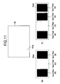
- FIG. 11 is a diagram representing a pixel configuration example according to an exemplary embodiment of the present invention.
- FIGS. 12 and 13 are block diagrams of a compensation example for R, G, B, W pixels according to an exemplary embodiment of the present invention.
- FIG. 4 shows a picture quality controlling method of a flat panel display device according to an exemplary embodiment of the present invention.
- the picture quality controlling method of the flat panel display device according to an exemplary embodiment of the present invention measures a screen state after applying an input signal to a sample flat panel display device using measuring equipment, such as a camera or the like.
- measuring equipment such as a camera or the like.
- step S 1 the image displayed on the sample flat panel display device is measured with measuring equipment, such as a camera or the like, having a resolution higher than the sample flat panel display device while increasing the input signal of the sample flat panel display device by one gray level starting from the lowest gray level (black) to the highest gray level (white).
- measuring equipment such as a camera or the like
- an input signal of 8 bits, for example, for each of RGB signals is received while a total of 256 screens from 0 to 255 gray level is measured for a sample flat panel display device having a resolution of 1366 ⁇ 768, for example.
- each of the measured screens should have a resolution of 1366 ⁇ 768 or more, and the brightness should have the resolution of at least 8 bits or more, based on this example.
- the picture quality controlling method of the flat panel display device judges the presence or absence of the panel defects. If the panel defects are detected in the sample flat panel display device, a compensation value to correct the brightness and/or color difference of the panel defect is established. (S 2 ) The input video data is then modulated with the compensation value to compensate for the brightness and/or color difference at the panel defect location. (S 3 )
- step S 2 the location and degree of the panel defect for each gray level are determined from the measured results of step S, and the compensation value is determined therefrom.
- the compensation value is optimized for each location since the degree of unevenness in brightness and/or color difference may be different for each location of the panel defect. Additionally, the compensation value is optimized for each gray level in consideration of gamma characteristics.
- the compensation value can be set for each gray level or for each gray level section (A, B, C, D), which includes a plurality of gray levels.
- a compensation value may be set for each gray level in the following exemplary manner: “+1” may be set in the location of “panel defect 1 ,” “ ⁇ 1” may be set in the location of “panel defect 2 ,” “0” may be set in the location of “panel defect 3 ,” and so on.
- the compensation value may be set for each gray level section in the following exemplary manner: “0” in “gray level section A,” “0” in “gray level section B,” “1” in “gray level section C,” “1” in “gray level section D,” and so on. Accordingly, the compensation value can be made different in the same panel defect location for each gray level and can also be different in the same gray level for each panel defect location.
- the compensation values are set to be the same value in each of R, G, B data of one pixel.
- the compensation values are set for each pixel inclusive of R, G, B sub-pixels.
- the compensation value is set differently for each of the R, G, B data. For example, if the red color appears more conspicuous in a specific panel defect location than in the non-defect location, an R compensation value may be set to be smaller than G, B compensation values.
- the compensation values may be arranged in a lookup table along with the panel defect location data and stored in a non-volatile memory.
- step S 3 the compensation values established in step S 2 are selectively added to or subtracted from the input digital video data to be displayed at the panel defect location, thereby modulating the corresponding digital video data.
- step S 3 the display location and gray level of the input digital video data are analyzed and a display spot is compensated by adding to or subtracting from the input digital video data a pre-set compensation value if the input digital video data is judged to be the data which is to be displayed in the panel defect location.
- a display location of the input digital video data is compared with the panel defect location stored in the non-volatile memory. If the comparison determines that the display location for the input digital video data is a panel defect location, the compensation value stored for the location in the non-volatile memory is applied to the input digital video data. For example, if the compensation value according to the gray level of the panel defect location is set as “2,” the display spot is compensated by adding a “2” to the input digital video data the compensation to increase the input digital video data to be displayed at the panel defect location by two gray levels.
- the display spot is compensated by adding “ ⁇ 2” to the input digital video data to be displayed in the panel defect location to decrease the input digital video data to be displayed at the panel defect location by two gray levels.
- the flat panel display device includes a compensation circuit 105 that receives the video data, modulates the video data, and then supplies the modulated video data to a driving part 110 of a display panel 103 .
- FIG. 7 shows a liquid crystal display device according to an exemplary embodiment of the present invention.
- the liquid crystal display device includes a liquid crystal display panel 103 having data lines 106 cross gate lines 108 with a thin-film transistor (TFT) formed at each intersection to drive a liquid crystal cell (Clc). Further, a compensation circuit 105 to generate a corrected digital video data Rc/Gc/Bc, a data drive circuit 101 to supply the data line 106 with the corrected digital video data Rc/Gc/Bc, a gate drive circuit 102 to supply a scan pulse to the gate lines 108 , and a timing controller 104 to control the data drive circuit 101 and the gate drive circuit 102 are also included.
- TFT thin-film transistor
- the liquid crystal display panel 103 includes two substrates, typically a TFT substrate and a color filter substrate, with liquid crystal molecules injected between the two substrates.
- the data lines 106 and the gate lines 108 are typically formed on the TFT substrate cross and each other.
- the TFTs formed at the crossing parts of the data lines 106 and the gate lines 108 supply an analog gamma compensation voltage supplied through the data line 106 to a pixel electrode (not shown) of the liquid crystal cell Clc in response to a scan signal from the gate line 108 .
- a black matrix, a color filter, and a common electrode are formed on the color filter substrate.
- One pixel on the liquid crystal display panel 103 includes a red (R) sub-pixel, a green (G) sub-pixel, and a blue (B) sub-pixel.
- the common electrode formed on the color filter substrate may alternatively be formed on the TFT substrate depending on an electric field application method.
- Polarizers having vertical polarizing axes and perpendicular to each other are respectively attached to the TFT substrate and the color filter substrate.
- the compensation circuit 105 receives the input digital video data Ri/Gi/Bi from a system interface to modulate the input digital video data Ri/Gi/Bi, which are to be supplied to the panel defect location, to generate the corrected digital video data Rc/Gc/Bc.
- the compensation circuit 105 is described in more detailed below.
- the timing controller 104 generates a gate control signal (GDC) to control the gate drive circuit 102 and a data control signal (DDC) to control the data drive circuit 101 based on a vertical synchronization signal (Vsync), a horizontal synchronization signal (Hsync), a data enable signal (DE), and a dot clock signal (DCLK) supplied through the compensation circuit 105 . Further, the timing controller 104 supplies the corrected digital video data Rc/Gc/Bc to the data drive circuit 101 in accordance with the dot clock signal (DCLK).
- GDC gate control signal
- DDC data control signal
- the data drive circuit 101 receives the corrected digital video data Rc/Gc/Bc, converts the digital video data Rc/Gc/Bc into an analog gamma compensation voltage, and supplies the analog voltages to the data lines 106 of the liquid crystal display panel 103 under control of the timing controller 104 to drive each of the liquid crystal cells (Clc).
- the gate drive circuit 102 supplies a scan signal to the gate lines 108 , thereby turning on the TFT's connected to the gate lines 108 to select the liquid crystal cells (Clc) of one horizontal line to which the analog gamma compensation voltage is to be supplied.
- the analog gamma compensation voltage generated from the data drive circuit 101 is synchronized with the scan pulse to be supplied to the liquid crystal cells (Clc) of the selected one horizontal line.
- the compensation circuit 105 includes a memory 116 in which the location and compensation value of a panel defect are stored, a modulator 115 to generate the corrected digital video data Rc, Gc, Bc by modulating the input signal Ri, Gi, Bi with the location and compensation value stored in the memory 116 , an interface circuit 117 to communicate between the compensation circuit 105 and an external system, and a register 118 to temporarily store the location and compensation value of the panel defect that are to be stored at the memory 116 .
- the compensation value in accordance with the gray level of the input digital video data Ri/Gi/Bi for each location of the panel defects are stored at the memory 116 along with the location of the panel defect. More specifically, the compensation value in accordance with the gray level may be a compensation value corresponding to each gray level, or the compensation value may be set in correspondence to a gray level section, which includes two or more gray levels.
- the memory 116 may be a non-volatile memory.
- the memory 11 may be an electrically erasable programmable read-only memory (EEPROM) with which the data for the compensation value and location of the panel defect may be updated by electrical signals from the external system.
- EEPROM electrically erasable programmable read-only memory
- EDID ROM extended display identification data read-only memory
- the EDI ROM stores the panel defect compensation-related data in addition to monitor information data, such as seller/manufacturer identification information and variables, characteristics, and other data related to the display device.
- a ROM recorder (not shown) transfers the panel defect compensation data through a data display channel (DDC).
- DDC data display channel
- the interface circuit 117 is configured to allow communication between the compensation circuit 105 and the external system (not shown) using a standard communication protocol, such as I2C, and the like.
- the external system (not shown) has access to the data stored in the memory 116 through the interface circuit 117 to read or modify the stored data.
- the compensation value data (CD) and the pixel location data (PD) of a panel defect stored in the memory 116 may be updated based on process changes, difference between application models, and the like.
- user-supplied compensation value data (UCD) and pixel location data (UPD) input from the external system (not shown) may be used to modify the data stored in the memory 116 .
- UPD pixel location data
- UPD compensation value data
- UPD pixel location data
- the pixel location data (UPD) and compensation value data (UCD) transmitted through the interface circuit 117 are temporarily stored in the register 118 in order to update the memory 116 .
- the modulator 115 determines whether or not the input digital video data Ri/Bi/Gi are video data to be supplied to the location of the panel defect based on the information stored in the memory 116 . If the modulator 115 determines that the input digital video data Ri/Bi/Gi are video data to be supplied to a panel defect location, the modulator 115 reads the compensation value of each gray level at the location of the panel defect from the memory 116 to generate the corrected digital video data Rc/Bc/Gc.
- the modulator 115 will be described with reference to FIG. 9 .
- the modulator 115 includes a location finding module to determine the location of the input digital video data Ri/Gi/Bi based on the vertical and horizontal synchronization signals (Vsync, Hsync), the data enable signal (DE), and the dot clock signal (DCLK). If the location of the input digital video data Ri/Gi/Bi corresponds to a panel defect location stored in the memory 116 , the gray level area of the input digital video data Ri/Gi/Bi and the location data is analyzed to generate an address value for reading the compensation data from the memory 116 .
- the compensation value data (R_increase/decrease amount, G_increase/decrease amount, B_increase/decrease amount) in accordance with the gray level of the input digital video data Ri/Gi/Bi at each location of the panel defect are stored at a specified address of the memory 116 . Accordingly, the input digital video data Ri/Gi/Bi are increased or decreased in accordance with the compensation value data obtained from a specified address corresponding to the panel defect location to generate the corrected video data Rc/Gc/Bc.
- the compensation value data (R_increase/decrease amount, G_increase/decrease amount, B_increase/decrease amount) for one pixel in the same panel defect location and the same gray level may be set to be the same (i.e., an R compensation value for compensating red data, a G compensation value for compensating green data, and B compensation value for compensating blue data are all the same), or at least any one of the R compensation value, the G compensation value, and the B compensation value may be set to be different from the others depending on the correction needed at the panel defect location.
- all three compensation values i.e., R compensation value, G compensation value, B compensation value
- all three colors are equally increased in strength for this pixel location.
- a compensation value increased by one gray level is set as the R compensation value and a compensation value increased by zero gray level is set as the G compensation value and the B compensation value. That is to say, the R sub-pixel may be compensated with an increase of one gray level while no gray level compensation is made for the G sub-pixel and the B sub-pixel. Accordingly, the pixel with the R sub-pixel may be corrected to display a stronger red color. In this way, color correction may be made on a pixel-by-pixel basis.
- FIG. 11 shows a diagram representing various pixel configurations.
- a pixel is a minimum unit of a screen needed to display an image.
- a pixel may include three sub-pixels R, G, B (sub-pixel (R), sub-pixel (G), sub-pixel (B)) as shown in portion (a) of FIG. 11 .
- a pixel may include four sub-pixels R, G, B, W (sub-pixel (R), sub-pixel (G), sub-pixel (B), sub-pixel (W)) with sub-pixel (W) expressing white, as shown in portion (b) of FIG. 11 .
- gray level correction of a panel defect may be performed by compensating only the W sub-pixel, as shown in FIG. 12 . If both gray level and color correction are needed, the gray level compensation and the color difference correction can be made at the same time by applying the compensation values to each of the R, G, B, W sub-pixels, as shown in FIG. 13 .
- the exemplary embodiment of the present invention has been described in relation to a liquid crystal display device.
- other flat panel display devices may be used without departing from the scope of the invention.
- the compensation circuit 105 as described above may be integrated with the timing controller 104 on a single chip.
- Other circuit arrangements may be used without departing from the scope of the present invention.
- the flat panel display device and the picture quality controlling method thereof according to the present invention electrically compensates for panel defects, and as a result, it is possible to improve the display quality in the display panel where the panel defect exists.
Abstract
Description
Claims (22)
Applications Claiming Priority (3)
| Application Number | Priority Date | Filing Date | Title |
|---|---|---|---|
| KR1020050097618A KR101136286B1 (en) | 2005-10-17 | 2005-10-17 | Flat Display Apparatus And Picture Quality Controling Method Thereof |
| KR10-2005-0097618 | 2005-10-17 | ||
| KRP2005-0097618 | 2005-10-17 |
Publications (2)
| Publication Number | Publication Date |
|---|---|
| US20070085790A1 US20070085790A1 (en) | 2007-04-19 |
| US7834836B2 true US7834836B2 (en) | 2010-11-16 |
Family
ID=37947714
Family Applications (1)
| Application Number | Title | Priority Date | Filing Date |
|---|---|---|---|
| US11/477,386 Active 2028-11-09 US7834836B2 (en) | 2005-10-17 | 2006-06-30 | Flat display apparatus and picture quality controlling method thereof |
Country Status (5)
| Country | Link |
|---|---|
| US (1) | US7834836B2 (en) |
| JP (1) | JP4787081B2 (en) |
| KR (1) | KR101136286B1 (en) |
| CN (1) | CN100420982C (en) |
| TW (1) | TWI345187B (en) |
Cited By (4)
| Publication number | Priority date | Publication date | Assignee | Title |
|---|---|---|---|---|
| US20120146995A1 (en) * | 2010-12-09 | 2012-06-14 | Jeongki Lee | Stereoscopic image display and method for driving the same |
| US20150145841A1 (en) * | 2013-11-28 | 2015-05-28 | Samsung Electronics Co., Ltd. | Apparatus and method for generating correction data, and image quality correction system thereof |
| US9824616B2 (en) | 2015-03-09 | 2017-11-21 | Shenzhen China Star Optoelectronics Technology Co., Ltd | Drive method and drive device of liquid crystal display |
| US10319315B2 (en) * | 2016-10-10 | 2019-06-11 | Shenzhen China Star Optoelectronics Technology Co., Ltd | Liquid crystal display and a compensation data storage method thereof |
Families Citing this family (30)
| Publication number | Priority date | Publication date | Assignee | Title |
|---|---|---|---|---|
| US8036456B2 (en) * | 2006-09-13 | 2011-10-11 | Hewlett-Packard Development Company, L.P. | Masking a visual defect |
| JP5229713B2 (en) * | 2007-01-29 | 2013-07-03 | 株式会社ジャパンディスプレイイースト | Display device |
| KR101362145B1 (en) * | 2007-05-16 | 2014-02-12 | 엘지디스플레이 주식회사 | Memory Interface Device And Flat Panel Display And Driving Method Thereof Using It |
| TWI363330B (en) * | 2007-05-24 | 2012-05-01 | Au Optronics Corp | Pulse generation circuit and display apparatus for adjusting display brightness of a picture |
| US10810918B2 (en) * | 2007-06-14 | 2020-10-20 | Lg Display Co., Ltd. | Video display device capable of compensating for display defects |
| KR101286537B1 (en) * | 2007-06-14 | 2013-07-17 | 엘지디스플레이 주식회사 | Video display device for compensating display defect |
| US9342266B2 (en) | 2007-08-08 | 2016-05-17 | Landmark Screens, Llc | Apparatus for dynamically circumventing faults in the light emitting diodes (LEDs) of a pixel in a graphical display |
| US8243090B2 (en) * | 2007-08-08 | 2012-08-14 | Landmark Screens, Llc | Method for mapping a color specified using a smaller color gamut to a larger color gamut |
| US9262118B2 (en) * | 2007-08-08 | 2016-02-16 | Landmark Screens, Llc | Graphical display comprising a plurality of modules each controlling a group of pixels corresponding to a portion of the graphical display |
| US9536463B2 (en) * | 2007-08-08 | 2017-01-03 | Landmark Screens, Llc | Method for fault-healing in a light emitting diode (LED) based display |
| US9779644B2 (en) * | 2007-08-08 | 2017-10-03 | Landmark Screens, Llc | Method for computing drive currents for a plurality of LEDs in a pixel of a signboard to achieve a desired color at a desired luminous intensity |
| US9659513B2 (en) * | 2007-08-08 | 2017-05-23 | Landmark Screens, Llc | Method for compensating for a chromaticity shift due to ambient light in an electronic signboard |
| US9620038B2 (en) * | 2007-08-08 | 2017-04-11 | Landmark Screens, Llc | Method for displaying a single image for diagnostic purpose without interrupting an observer's perception of the display of a sequence of images |
| US7768180B2 (en) * | 2007-08-08 | 2010-08-03 | Landmark Screens, Llc | Enclosure for housing a plurality of pixels of a graphical display |
| KR101308465B1 (en) * | 2008-06-04 | 2013-09-16 | 엘지디스플레이 주식회사 | Video display device for compensating display defect |
| KR101274707B1 (en) * | 2008-06-05 | 2013-06-12 | 엘지디스플레이 주식회사 | Compensation circuit of video display device for compensating display defect and method thereof |
| KR101323457B1 (en) * | 2008-12-10 | 2013-10-29 | 엘지디스플레이 주식회사 | Method and Apparatus for Compensating Display Defect of Flat Display |
| KR102151262B1 (en) | 2013-09-11 | 2020-09-03 | 삼성디스플레이 주식회사 | Method of driving a display panel, display apparatus performing the same, method of calculating a correction value applied to the same and method of correcting gray data |
| KR20150073370A (en) * | 2013-12-23 | 2015-07-01 | 주식회사 코윈디에스티 | Appratus for repairing curved panel display defect |
| KR102125873B1 (en) * | 2013-12-31 | 2020-06-23 | 엘지디스플레이 주식회사 | Display device and gamma compensation method thereof |
| KR102180683B1 (en) | 2014-07-21 | 2020-11-20 | 삼성디스플레이 주식회사 | Method of displaying an image, display apparatus performing the same, method of calculating a correction value applied to the same and method of correcting gray data |
| KR102255299B1 (en) * | 2014-11-03 | 2021-05-24 | 엘지디스플레이 주식회사 | Timing controller, display panel, and display panel |
| CN104537990A (en) * | 2014-12-24 | 2015-04-22 | 深圳市华星光电技术有限公司 | Method and device for improving display image uniformity |
| KR102469305B1 (en) * | 2015-08-17 | 2022-11-23 | 삼성디스플레이 주식회사 | Display driving integrated circuit, display device, and method of driving a display device |
| CN106531045B (en) * | 2015-09-11 | 2021-06-22 | 三星电子株式会社 | Time schedule controller and display device comprising same |
| KR102459249B1 (en) * | 2015-12-31 | 2022-10-26 | 엘지디스플레이 주식회사 | Terminal for correcting afterimage area and method and apparatus for coreecting afterimage area using the same |
| CN107977182A (en) * | 2017-12-07 | 2018-05-01 | 深圳吉迪思电子科技有限公司 | A kind of display screen drive system and method |
| WO2020183699A1 (en) * | 2019-03-14 | 2020-09-17 | Necディスプレイソリューションズ株式会社 | Electronic apparatus and method for controlling electronic apparatus |
| CN110992887B (en) * | 2019-12-26 | 2021-03-30 | 昆山国显光电有限公司 | Mura compensation data acquisition method and device and display device |
| US20220035675A1 (en) * | 2020-08-02 | 2022-02-03 | Avatar Cognition Barcelona S.L. | Pattern recognition system utilizing self-replicating nodes |
Citations (19)
| Publication number | Priority date | Publication date | Assignee | Title |
|---|---|---|---|---|
| JPH07261710A (en) | 1994-03-25 | 1995-10-13 | Matsushita Electric Ind Co Ltd | Liquid crystal driving device |
| JP2001231053A (en) | 2000-02-15 | 2001-08-24 | Sony Corp | Method for generating correction data in image display device |
| JP2001331156A (en) | 2000-03-17 | 2001-11-30 | Hitachi Ltd | Liquid crystal display device |
| US20020067326A1 (en) * | 2000-12-01 | 2002-06-06 | Seiko Epson Corporation | Liquid crystal display, image data compensation circuit, image data compensation method, and electronic apparatus |
| JP2002366109A (en) | 2001-06-06 | 2002-12-20 | Victor Co Of Japan Ltd | Active matrix type liquid crystal display device |
| US20030098839A1 (en) * | 2001-11-26 | 2003-05-29 | Lee Baek-Woon | Liquid crystal display and a driving method thereof |
| US6603452B1 (en) * | 1999-02-01 | 2003-08-05 | Kabushiki Kaisha Toshiba | Color shading correction device and luminance shading correction device |
| JP2004062134A (en) | 2002-06-03 | 2004-02-26 | Sharp Corp | Liquid crystal display |
| US6704008B2 (en) * | 2000-01-26 | 2004-03-09 | Seiko Epson Corporation | Non-uniformity correction for displayed images |
| JP2004153532A (en) | 2002-10-30 | 2004-05-27 | Sanyo Electric Co Ltd | Gamma correction data rewrite device |
| JP2004177827A (en) | 2002-11-28 | 2004-06-24 | Sharp Corp | Device for driving liquid crystal |
| US6847342B2 (en) * | 1999-07-08 | 2005-01-25 | Nichia Corporation | Image display apparatus |
| US20050062735A1 (en) * | 2003-09-23 | 2005-03-24 | Samsung Electronics Co., Ltd. | Display unit and control method thereof |
| US20050093798A1 (en) * | 2003-10-29 | 2005-05-05 | Fujitsu Display Technologies Corporation | Correction of uneven image appearance by use of small-size data |
| JP2005134864A (en) | 2003-10-28 | 2005-05-26 | Renei Kagi Kofun Yugenkoshi | Liquid crystal display panel and its driving circuit |
| US20050116917A1 (en) * | 2003-11-12 | 2005-06-02 | Seiko Epson Corporation | Method of correcting unevenness of brightness, correction circuit for correcting unevenness of brightness, electro-optical device, and electronic apparatus |
| US20050140622A1 (en) * | 2003-12-30 | 2005-06-30 | Lee Han S. | Apparatus and method for driving liquid crystal display device |
| US6946886B2 (en) * | 2002-12-04 | 2005-09-20 | Denso Corporation | Clock-synchronized serial communication device and semiconductor integrated circuit device |
| US7009627B2 (en) * | 2001-11-21 | 2006-03-07 | Canon Kabushiki Kaisha | Display apparatus, and image signal processing apparatus and drive control apparatus for the same |
Family Cites Families (14)
| Publication number | Priority date | Publication date | Assignee | Title |
|---|---|---|---|---|
| JPS61137194A (en) * | 1984-12-10 | 1986-06-24 | キヤノン株式会社 | Correction/driving of liquid crystal display panel |
| JPS61243495A (en) * | 1985-04-20 | 1986-10-29 | 三洋電機株式会社 | Compensation of uneven display for liquid crystal display unit |
| JPH06138486A (en) * | 1992-10-28 | 1994-05-20 | Toshiba Corp | Liquid crystal display device and its driving method |
| JPH06138849A (en) * | 1992-10-30 | 1994-05-20 | Sharp Corp | Liquid crystal video display device |
| JPH06195048A (en) * | 1992-11-09 | 1994-07-15 | Sony Corp | Device for compensating defective pixel |
| JP3672586B2 (en) * | 1994-03-24 | 2005-07-20 | 株式会社半導体エネルギー研究所 | Correction system and operation method thereof |
| JPH08179727A (en) * | 1994-12-20 | 1996-07-12 | Fujitsu General Ltd | Liquid crystal projector |
| JP2000209603A (en) * | 1999-01-12 | 2000-07-28 | Nec Corp | Device for correcting uneven color and method for correcting uneven color |
| JP2000341716A (en) * | 1999-05-31 | 2000-12-08 | Matsushita Electric Ind Co Ltd | Gradation correction circuit and its correction method |
| TW575855B (en) * | 1999-08-05 | 2004-02-11 | Sharp Kk | Display device |
| JP2001209351A (en) * | 2000-01-28 | 2001-08-03 | Sanyo Electric Co Ltd | Projection type video display device |
| US7227596B2 (en) * | 2001-06-23 | 2007-06-05 | Thomson Licensing | Colour defects in a display panel due to different time response of phosphors |
| CN1209662C (en) * | 2001-12-17 | 2005-07-06 | 精工爱普生株式会社 | Display device and electronic apparatus |
| KR100910557B1 (en) * | 2002-11-12 | 2009-08-03 | 삼성전자주식회사 | Liquid crystal display and driving method thereof |
-
2005
- 2005-10-17 KR KR1020050097618A patent/KR101136286B1/en active IP Right Grant
-
2006
- 2006-05-29 TW TW095119039A patent/TWI345187B/en active
- 2006-06-05 CN CNB200610083543XA patent/CN100420982C/en active Active
- 2006-06-15 JP JP2006166501A patent/JP4787081B2/en active Active
- 2006-06-30 US US11/477,386 patent/US7834836B2/en active Active
Patent Citations (19)
| Publication number | Priority date | Publication date | Assignee | Title |
|---|---|---|---|---|
| JPH07261710A (en) | 1994-03-25 | 1995-10-13 | Matsushita Electric Ind Co Ltd | Liquid crystal driving device |
| US6603452B1 (en) * | 1999-02-01 | 2003-08-05 | Kabushiki Kaisha Toshiba | Color shading correction device and luminance shading correction device |
| US6847342B2 (en) * | 1999-07-08 | 2005-01-25 | Nichia Corporation | Image display apparatus |
| US6704008B2 (en) * | 2000-01-26 | 2004-03-09 | Seiko Epson Corporation | Non-uniformity correction for displayed images |
| JP2001231053A (en) | 2000-02-15 | 2001-08-24 | Sony Corp | Method for generating correction data in image display device |
| JP2001331156A (en) | 2000-03-17 | 2001-11-30 | Hitachi Ltd | Liquid crystal display device |
| US20020067326A1 (en) * | 2000-12-01 | 2002-06-06 | Seiko Epson Corporation | Liquid crystal display, image data compensation circuit, image data compensation method, and electronic apparatus |
| JP2002366109A (en) | 2001-06-06 | 2002-12-20 | Victor Co Of Japan Ltd | Active matrix type liquid crystal display device |
| US7009627B2 (en) * | 2001-11-21 | 2006-03-07 | Canon Kabushiki Kaisha | Display apparatus, and image signal processing apparatus and drive control apparatus for the same |
| US20030098839A1 (en) * | 2001-11-26 | 2003-05-29 | Lee Baek-Woon | Liquid crystal display and a driving method thereof |
| JP2004062134A (en) | 2002-06-03 | 2004-02-26 | Sharp Corp | Liquid crystal display |
| JP2004153532A (en) | 2002-10-30 | 2004-05-27 | Sanyo Electric Co Ltd | Gamma correction data rewrite device |
| JP2004177827A (en) | 2002-11-28 | 2004-06-24 | Sharp Corp | Device for driving liquid crystal |
| US6946886B2 (en) * | 2002-12-04 | 2005-09-20 | Denso Corporation | Clock-synchronized serial communication device and semiconductor integrated circuit device |
| US20050062735A1 (en) * | 2003-09-23 | 2005-03-24 | Samsung Electronics Co., Ltd. | Display unit and control method thereof |
| JP2005134864A (en) | 2003-10-28 | 2005-05-26 | Renei Kagi Kofun Yugenkoshi | Liquid crystal display panel and its driving circuit |
| US20050093798A1 (en) * | 2003-10-29 | 2005-05-05 | Fujitsu Display Technologies Corporation | Correction of uneven image appearance by use of small-size data |
| US20050116917A1 (en) * | 2003-11-12 | 2005-06-02 | Seiko Epson Corporation | Method of correcting unevenness of brightness, correction circuit for correcting unevenness of brightness, electro-optical device, and electronic apparatus |
| US20050140622A1 (en) * | 2003-12-30 | 2005-06-30 | Lee Han S. | Apparatus and method for driving liquid crystal display device |
Cited By (5)
| Publication number | Priority date | Publication date | Assignee | Title |
|---|---|---|---|---|
| US20120146995A1 (en) * | 2010-12-09 | 2012-06-14 | Jeongki Lee | Stereoscopic image display and method for driving the same |
| US20150145841A1 (en) * | 2013-11-28 | 2015-05-28 | Samsung Electronics Co., Ltd. | Apparatus and method for generating correction data, and image quality correction system thereof |
| US9898998B2 (en) * | 2013-11-28 | 2018-02-20 | Samsung Electronics Co., Ltd. | Apparatus and method for generating correction data, and image quality correction system thereof |
| US9824616B2 (en) | 2015-03-09 | 2017-11-21 | Shenzhen China Star Optoelectronics Technology Co., Ltd | Drive method and drive device of liquid crystal display |
| US10319315B2 (en) * | 2016-10-10 | 2019-06-11 | Shenzhen China Star Optoelectronics Technology Co., Ltd | Liquid crystal display and a compensation data storage method thereof |
Also Published As
| Publication number | Publication date |
|---|---|
| TW200717385A (en) | 2007-05-01 |
| KR101136286B1 (en) | 2012-04-19 |
| CN1952735A (en) | 2007-04-25 |
| KR20070041942A (en) | 2007-04-20 |
| JP4787081B2 (en) | 2011-10-05 |
| CN100420982C (en) | 2008-09-24 |
| JP2007114733A (en) | 2007-05-10 |
| US20070085790A1 (en) | 2007-04-19 |
| TWI345187B (en) | 2011-07-11 |
Similar Documents
| Publication | Publication Date | Title |
|---|---|---|
| US7834836B2 (en) | Flat display apparatus and picture quality controlling method thereof | |
| US7786971B2 (en) | Flat display apparatus capable of compensating a panel defect electrically and picture quality controlling method thereof | |
| JP4638384B2 (en) | Flat panel display and image quality control method thereof | |
| KR101201314B1 (en) | Method of Fabricating Flat Display Panel | |
| US7791572B2 (en) | Flat display panel, picture quality controlling apparatus and method thereof | |
| US7847772B2 (en) | Fabricating method and fabricating apparatus thereof, and picture quality controlling method and apparatus thereof | |
| US7889165B2 (en) | Flat display apparatus, fabricating method, picture quality controlling method and apparatus thereof | |
| US8648883B2 (en) | Display apparatus and method of driving the same | |
| US8189017B2 (en) | Apparatus and method for controlling picture quality of flat panel display | |
| US8378941B2 (en) | Liquid crystal display device and method of driving the same | |
| KR101329074B1 (en) | Apparatus And Method For Controling Picture Quality of Flat Panel Display | |
| KR101296655B1 (en) | Circuit of compensating data in video display device and method thereof | |
| KR101286537B1 (en) | Video display device for compensating display defect | |
| KR100610620B1 (en) | Liquid crystal display device and white balance correcting method thereof |
Legal Events
| Date | Code | Title | Description |
|---|---|---|---|
| AS | Assignment |
Owner name: LG.PHILIPS LCD CO., LTD., KOREA, REPUBLIC OF Free format text: ASSIGNMENT OF ASSIGNORS INTEREST;ASSIGNORS:CHUNG, IN JAE;JANG, CHUL SANG;JO, SUNG HAK;AND OTHERS;SIGNING DATES FROM 20060625 TO 20060629;REEL/FRAME:018069/0901 Owner name: LG.PHILIPS LCD CO., LTD., KOREA, REPUBLIC OF Free format text: ASSIGNMENT OF ASSIGNORS INTEREST;ASSIGNORS:CHUNG, IN JAE;JANG, CHUL SANG;JO, SUNG HAK;AND OTHERS;REEL/FRAME:018069/0901;SIGNING DATES FROM 20060625 TO 20060629 |
|
| AS | Assignment |
Owner name: LG DISPLAY CO., LTD., KOREA, REPUBLIC OF Free format text: CHANGE OF NAME;ASSIGNOR:LG.PHILIPS LCD CO., LTD.;REEL/FRAME:021147/0009 Effective date: 20080319 Owner name: LG DISPLAY CO., LTD.,KOREA, REPUBLIC OF Free format text: CHANGE OF NAME;ASSIGNOR:LG.PHILIPS LCD CO., LTD.;REEL/FRAME:021147/0009 Effective date: 20080319 |
|
| STCF | Information on status: patent grant |
Free format text: PATENTED CASE |
|
| FEPP | Fee payment procedure |
Free format text: PAYOR NUMBER ASSIGNED (ORIGINAL EVENT CODE: ASPN); ENTITY STATUS OF PATENT OWNER: LARGE ENTITY |
|
| FPAY | Fee payment |
Year of fee payment: 4 |
|
| MAFP | Maintenance fee payment |
Free format text: PAYMENT OF MAINTENANCE FEE, 8TH YEAR, LARGE ENTITY (ORIGINAL EVENT CODE: M1552) Year of fee payment: 8 |
|
| MAFP | Maintenance fee payment |
Free format text: PAYMENT OF MAINTENANCE FEE, 12TH YEAR, LARGE ENTITY (ORIGINAL EVENT CODE: M1553); ENTITY STATUS OF PATENT OWNER: LARGE ENTITY Year of fee payment: 12 |