US7803017B2 - Simultaneous bidirectional cable interface - Google Patents
Simultaneous bidirectional cable interface Download PDFInfo
- Publication number
- US7803017B2 US7803017B2 US11/653,929 US65392907A US7803017B2 US 7803017 B2 US7803017 B2 US 7803017B2 US 65392907 A US65392907 A US 65392907A US 7803017 B2 US7803017 B2 US 7803017B2
- Authority
- US
- United States
- Prior art keywords
- cable
- circuit
- cable module
- connection
- circuits
- Prior art date
- Legal status (The legal status is an assumption and is not a legal conclusion. Google has not performed a legal analysis and makes no representation as to the accuracy of the status listed.)
- Expired - Fee Related, expires
Links
- 230000002457 bidirectional effect Effects 0.000 title claims abstract description 40
- 239000004020 conductor Substances 0.000 claims abstract description 53
- 230000011664 signaling Effects 0.000 claims description 29
- 238000004519 manufacturing process Methods 0.000 abstract description 14
- 238000000034 method Methods 0.000 description 29
- 238000004806 packaging method and process Methods 0.000 description 13
- 239000000463 material Substances 0.000 description 11
- 230000005540 biological transmission Effects 0.000 description 6
- 238000005516 engineering process Methods 0.000 description 6
- 239000004593 Epoxy Substances 0.000 description 5
- 238000011161 development Methods 0.000 description 5
- 239000011347 resin Substances 0.000 description 5
- 229920005989 resin Polymers 0.000 description 5
- 238000012546 transfer Methods 0.000 description 5
- XUIMIQQOPSSXEZ-UHFFFAOYSA-N Silicon Chemical compound [Si] XUIMIQQOPSSXEZ-UHFFFAOYSA-N 0.000 description 4
- 238000013461 design Methods 0.000 description 4
- 229910052710 silicon Inorganic materials 0.000 description 4
- 239000010703 silicon Substances 0.000 description 4
- 238000005476 soldering Methods 0.000 description 4
- 239000013307 optical fiber Substances 0.000 description 3
- 239000004033 plastic Substances 0.000 description 3
- 229920003023 plastic Polymers 0.000 description 3
- 239000004065 semiconductor Substances 0.000 description 3
- 230000002238 attenuated effect Effects 0.000 description 2
- 230000006854 communication Effects 0.000 description 2
- 238000004891 communication Methods 0.000 description 2
- 239000011888 foil Substances 0.000 description 2
- 230000002093 peripheral effect Effects 0.000 description 2
- 230000008054 signal transmission Effects 0.000 description 2
- 230000001629 suppression Effects 0.000 description 2
- 239000004698 Polyethylene Substances 0.000 description 1
- 239000000853 adhesive Substances 0.000 description 1
- 230000001070 adhesive effect Effects 0.000 description 1
- 229910052782 aluminium Inorganic materials 0.000 description 1
- XAGFODPZIPBFFR-UHFFFAOYSA-N aluminium Chemical compound [Al] XAGFODPZIPBFFR-UHFFFAOYSA-N 0.000 description 1
- 238000005452 bending Methods 0.000 description 1
- 230000007175 bidirectional communication Effects 0.000 description 1
- 238000007796 conventional method Methods 0.000 description 1
- 238000010586 diagram Methods 0.000 description 1
- 230000000694 effects Effects 0.000 description 1
- 230000008030 elimination Effects 0.000 description 1
- 238000003379 elimination reaction Methods 0.000 description 1
- PCHJSUWPFVWCPO-UHFFFAOYSA-N gold Chemical compound [Au] PCHJSUWPFVWCPO-UHFFFAOYSA-N 0.000 description 1
- 229910052737 gold Inorganic materials 0.000 description 1
- 239000010931 gold Substances 0.000 description 1
- 229910052751 metal Inorganic materials 0.000 description 1
- 239000002184 metal Substances 0.000 description 1
- 238000012986 modification Methods 0.000 description 1
- 230000004048 modification Effects 0.000 description 1
- 230000003287 optical effect Effects 0.000 description 1
- -1 polyethylene Polymers 0.000 description 1
- 229920000573 polyethylene Polymers 0.000 description 1
- 229910000679 solder Inorganic materials 0.000 description 1
- 239000007787 solid Substances 0.000 description 1
- 230000003068 static effect Effects 0.000 description 1
- 238000006467 substitution reaction Methods 0.000 description 1
- 239000000758 substrate Substances 0.000 description 1
- 230000001360 synchronised effect Effects 0.000 description 1
Images


Classifications
-
- H—ELECTRICITY
- H05—ELECTRIC TECHNIQUES NOT OTHERWISE PROVIDED FOR
- H05K—PRINTED CIRCUITS; CASINGS OR CONSTRUCTIONAL DETAILS OF ELECTRIC APPARATUS; MANUFACTURE OF ASSEMBLAGES OF ELECTRICAL COMPONENTS
- H05K1/00—Printed circuits
- H05K1/02—Details
- H05K1/0213—Electrical arrangements not otherwise provided for
- H05K1/0237—High frequency adaptations
- H05K1/0243—Printed circuits associated with mounted high frequency components
-
- H—ELECTRICITY
- H01—ELECTRIC ELEMENTS
- H01L—SEMICONDUCTOR DEVICES NOT COVERED BY CLASS H10
- H01L2224/00—Indexing scheme for arrangements for connecting or disconnecting semiconductor or solid-state bodies and methods related thereto as covered by H01L24/00
- H01L2224/01—Means for bonding being attached to, or being formed on, the surface to be connected, e.g. chip-to-package, die-attach, "first-level" interconnects; Manufacturing methods related thereto
- H01L2224/42—Wire connectors; Manufacturing methods related thereto
- H01L2224/44—Structure, shape, material or disposition of the wire connectors prior to the connecting process
- H01L2224/45—Structure, shape, material or disposition of the wire connectors prior to the connecting process of an individual wire connector
- H01L2224/45001—Core members of the connector
- H01L2224/45099—Material
- H01L2224/451—Material with a principal constituent of the material being a metal or a metalloid, e.g. boron (B), silicon (Si), germanium (Ge), arsenic (As), antimony (Sb), tellurium (Te) and polonium (Po), and alloys thereof
- H01L2224/45117—Material with a principal constituent of the material being a metal or a metalloid, e.g. boron (B), silicon (Si), germanium (Ge), arsenic (As), antimony (Sb), tellurium (Te) and polonium (Po), and alloys thereof the principal constituent melting at a temperature of greater than or equal to 400°C and less than 950°C
- H01L2224/45124—Aluminium (Al) as principal constituent
-
- H—ELECTRICITY
- H01—ELECTRIC ELEMENTS
- H01L—SEMICONDUCTOR DEVICES NOT COVERED BY CLASS H10
- H01L2224/00—Indexing scheme for arrangements for connecting or disconnecting semiconductor or solid-state bodies and methods related thereto as covered by H01L24/00
- H01L2224/01—Means for bonding being attached to, or being formed on, the surface to be connected, e.g. chip-to-package, die-attach, "first-level" interconnects; Manufacturing methods related thereto
- H01L2224/42—Wire connectors; Manufacturing methods related thereto
- H01L2224/47—Structure, shape, material or disposition of the wire connectors after the connecting process
- H01L2224/48—Structure, shape, material or disposition of the wire connectors after the connecting process of an individual wire connector
- H01L2224/4805—Shape
- H01L2224/4809—Loop shape
- H01L2224/48091—Arched
-
- H—ELECTRICITY
- H01—ELECTRIC ELEMENTS
- H01L—SEMICONDUCTOR DEVICES NOT COVERED BY CLASS H10
- H01L2224/00—Indexing scheme for arrangements for connecting or disconnecting semiconductor or solid-state bodies and methods related thereto as covered by H01L24/00
- H01L2224/01—Means for bonding being attached to, or being formed on, the surface to be connected, e.g. chip-to-package, die-attach, "first-level" interconnects; Manufacturing methods related thereto
- H01L2224/42—Wire connectors; Manufacturing methods related thereto
- H01L2224/47—Structure, shape, material or disposition of the wire connectors after the connecting process
- H01L2224/48—Structure, shape, material or disposition of the wire connectors after the connecting process of an individual wire connector
- H01L2224/481—Disposition
- H01L2224/48151—Connecting between a semiconductor or solid-state body and an item not being a semiconductor or solid-state body, e.g. chip-to-substrate, chip-to-passive
- H01L2224/48221—Connecting between a semiconductor or solid-state body and an item not being a semiconductor or solid-state body, e.g. chip-to-substrate, chip-to-passive the body and the item being stacked
- H01L2224/48225—Connecting between a semiconductor or solid-state body and an item not being a semiconductor or solid-state body, e.g. chip-to-substrate, chip-to-passive the body and the item being stacked the item being non-metallic, e.g. insulating substrate with or without metallisation
- H01L2224/48227—Connecting between a semiconductor or solid-state body and an item not being a semiconductor or solid-state body, e.g. chip-to-substrate, chip-to-passive the body and the item being stacked the item being non-metallic, e.g. insulating substrate with or without metallisation connecting the wire to a bond pad of the item
-
- H—ELECTRICITY
- H01—ELECTRIC ELEMENTS
- H01L—SEMICONDUCTOR DEVICES NOT COVERED BY CLASS H10
- H01L2924/00—Indexing scheme for arrangements or methods for connecting or disconnecting semiconductor or solid-state bodies as covered by H01L24/00
- H01L2924/10—Details of semiconductor or other solid state devices to be connected
- H01L2924/102—Material of the semiconductor or solid state bodies
- H01L2924/1025—Semiconducting materials
- H01L2924/10251—Elemental semiconductors, i.e. Group IV
- H01L2924/10253—Silicon [Si]
-
- H—ELECTRICITY
- H01—ELECTRIC ELEMENTS
- H01L—SEMICONDUCTOR DEVICES NOT COVERED BY CLASS H10
- H01L2924/00—Indexing scheme for arrangements or methods for connecting or disconnecting semiconductor or solid-state bodies as covered by H01L24/00
- H01L2924/30—Technical effects
- H01L2924/301—Electrical effects
- H01L2924/30107—Inductance
-
- H—ELECTRICITY
- H01—ELECTRIC ELEMENTS
- H01L—SEMICONDUCTOR DEVICES NOT COVERED BY CLASS H10
- H01L2924/00—Indexing scheme for arrangements or methods for connecting or disconnecting semiconductor or solid-state bodies as covered by H01L24/00
- H01L2924/30—Technical effects
- H01L2924/301—Electrical effects
- H01L2924/3011—Impedance
-
- H—ELECTRICITY
- H01—ELECTRIC ELEMENTS
- H01L—SEMICONDUCTOR DEVICES NOT COVERED BY CLASS H10
- H01L2924/00—Indexing scheme for arrangements or methods for connecting or disconnecting semiconductor or solid-state bodies as covered by H01L24/00
- H01L2924/30—Technical effects
- H01L2924/301—Electrical effects
- H01L2924/3025—Electromagnetic shielding
-
- H—ELECTRICITY
- H05—ELECTRIC TECHNIQUES NOT OTHERWISE PROVIDED FOR
- H05K—PRINTED CIRCUITS; CASINGS OR CONSTRUCTIONAL DETAILS OF ELECTRIC APPARATUS; MANUFACTURE OF ASSEMBLAGES OF ELECTRICAL COMPONENTS
- H05K2201/00—Indexing scheme relating to printed circuits covered by H05K1/00
- H05K2201/09—Shape and layout
- H05K2201/09209—Shape and layout details of conductors
- H05K2201/09654—Shape and layout details of conductors covering at least two types of conductors provided for in H05K2201/09218 - H05K2201/095
- H05K2201/09809—Coaxial layout
-
- H—ELECTRICITY
- H05—ELECTRIC TECHNIQUES NOT OTHERWISE PROVIDED FOR
- H05K—PRINTED CIRCUITS; CASINGS OR CONSTRUCTIONAL DETAILS OF ELECTRIC APPARATUS; MANUFACTURE OF ASSEMBLAGES OF ELECTRICAL COMPONENTS
- H05K2201/00—Indexing scheme relating to printed circuits covered by H05K1/00
- H05K2201/10—Details of components or other objects attached to or integrated in a printed circuit board
- H05K2201/10227—Other objects, e.g. metallic pieces
- H05K2201/10356—Cables
-
- H—ELECTRICITY
- H05—ELECTRIC TECHNIQUES NOT OTHERWISE PROVIDED FOR
- H05K—PRINTED CIRCUITS; CASINGS OR CONSTRUCTIONAL DETAILS OF ELECTRIC APPARATUS; MANUFACTURE OF ASSEMBLAGES OF ELECTRICAL COMPONENTS
- H05K2201/00—Indexing scheme relating to printed circuits covered by H05K1/00
- H05K2201/10—Details of components or other objects attached to or integrated in a printed circuit board
- H05K2201/10431—Details of mounted components
- H05K2201/10507—Involving several components
- H05K2201/1053—Mounted components directly electrically connected to each other, i.e. not via the PCB
-
- H—ELECTRICITY
- H05—ELECTRIC TECHNIQUES NOT OTHERWISE PROVIDED FOR
- H05K—PRINTED CIRCUITS; CASINGS OR CONSTRUCTIONAL DETAILS OF ELECTRIC APPARATUS; MANUFACTURE OF ASSEMBLAGES OF ELECTRICAL COMPONENTS
- H05K2201/00—Indexing scheme relating to printed circuits covered by H05K1/00
- H05K2201/10—Details of components or other objects attached to or integrated in a printed circuit board
- H05K2201/10613—Details of electrical connections of non-printed components, e.g. special leads
- H05K2201/10621—Components characterised by their electrical contacts
- H05K2201/10674—Flip chip
-
- H—ELECTRICITY
- H05—ELECTRIC TECHNIQUES NOT OTHERWISE PROVIDED FOR
- H05K—PRINTED CIRCUITS; CASINGS OR CONSTRUCTIONAL DETAILS OF ELECTRIC APPARATUS; MANUFACTURE OF ASSEMBLAGES OF ELECTRICAL COMPONENTS
- H05K2203/00—Indexing scheme relating to apparatus or processes for manufacturing printed circuits covered by H05K3/00
- H05K2203/04—Soldering or other types of metallurgic bonding
- H05K2203/049—Wire bonding
Definitions
- the present invention relates to an integrated cable module circuit, a cable connection for simultaneous bidirectional signaling comprising the integrated cable module circuit, the use of such integrated cable module circuit and of such cable connection and a method of manufacture for the integrated cable module circuit as well as the cable connection.
- Serial high-speed interfaces use typically one differential wire pair or one optical fiber, also called one lane, per direction. For instance, two pairs are used for bidirectional transmission, in data transmission as, for instance, in serial ATA (advanced technology attachment) and Peripheral Component Interconnect (PCI) Express (PCIe), which uses existing PCI programming concepts, but on a completely different and much faster serial physical-layer communications protocol.
- PCI Peripheral Component Interconnect Express
- each lane utilizes two unidirectional low voltage differential signaling pairs at 2.5 Gb/s. Transmit and receive are separate differential pairs, for a total of 4 data wires per lane. As with all high-speed serial transmission protocols, clocking information must be embedded in the signal.
- PCIe utilizes the very common 8B/10B encoding scheme to ensure that strings of consecutive ones or consecutive zeros are limited in length, so that the receiver does not lose track of where the bit edges are. This coding scheme replaces 8 uncoded (payload) bits of data with 10 (encoded) bits of transmitted data, consuming 20% of the overall electrical bandwidth.
- one lane may be used for both directions, by using of the lane with a time division access (time-shared) scheme, where given (or negotiated) time slots are used for transmission from end A to end B or vice versa, respectively, which is used in Universal serial Bus (USB), for example.
- time-shared time division access
- USB Universal serial Bus
- FIG. 1 The basic principle of simultaneous bidirectional signaling is illustrated in FIG. 1 . If unit A sends a pulse via cable 10 to unit B, part of the pulse reflects back to unit A from impedance discontinuities in connectors 21 , 22 , and impedance mismatch of the intended receiver 32 (and/or electro static discharge (ESD) suppression components (not shown)) at unit B. This results in only low bit rate signaling in simultaneous bidirectional links having connectors, as it is the case in all of the above-discussed applications.
- ESD electro static discharge
- one method to handle unwanted reflected signals on data connections is echo-cancellation.
- the signal driver 41 of unit A sends a pulse into the cable 10 , but at the same time the same pulse is supplied to reference input pins of receiving comparator 31 by means of replica driver 51 .
- the effect of the supplied pulse from the replica driver 51 to the receiving comparator 31 is illustrated for a single-ended signaling in FIG. 2 (left part of the Fig.).
- the detecting level of the receiving comparator 31 is changed with an equal amount as the (send) pulse changes the signal at the output of signal driver 41 .
- the receiving comparator 31 will not “see” the pulse sent by the signal driver 41 located at the same end of the cable 10 .
- One remaining problem in such typical echo-cancellation system is matching of load coming from the cable 10 having connectors to the load seen by the replica driver 51 .
- the reference level of the receiving comparator 31 does not match to the signal sent into cable 10 . Consequently, the difference (signal) is seen as signal by the receiving comparator 31 and thus is mixed with the intended signal sent from the opposite end of the cable, for example the unit B in FIG. 1 .
- certain embodiments of the invention relate to solutions for the above-discussed problems.
- certain embodiments provide a cable connection and a method of manufacture thereof enabling a high-speed serial simultaneous bidirectional signaling connection.
- a cable connection may include at least one cable as a wire conducted signal interconnection between two cable module circuits connected to conductors of the cable at respective ends of the cable, wherein at least signal wires of the conductors of the cable are directly and permanent electrical connected at each end of the cable with respective contacts of the respective cable module circuit, wherein the cable module circuits are arranged for simultaneous bidirectional signaling via the cable connection.
- a similar cable connection may be used inside an electronic device, where electronic circuits of the electronic device are located in respective parts of a housing of the electronic device, wherein the parts of the housing of the electronic device are mechanical connected to each other such that the parts of the housing of the electronic device may be moved with respect to each other, and wherein the cable connection is going through or arranged inside the mechanical connection.
- an integrated circuit may include contacts for interconnection of the integrated circuit, which is a cable module circuit arranged for simultaneous bidirectional signaling via a cable connection; wherein the cable module circuit is adapted to be connected to a cable for a wire conducted signal interconnection via the cable with another cable module circuit connected to conductors of the cable at the other end of the cable; wherein at least signal wires of the conductors of the cable are to be directly and permanent electrical connected to the cable module circuit.
- a method of manufacture includes cutting a cable to a required predetermined length; fabricating integrated cable module circuits which are arranged for simultaneous bidirectional signaling via the cable; and connecting directly with a permanent method conductors of the cable at each cable end with respective contacts of the respective integrated cable module circuits; wherein in fabricating of the integrated cable module circuits input and output impedances of the integrated cable module circuits connected to conductors of the cable are matched to the respective cable impedance.
- Certain embodiments relate to a method of manufacture including fabricating an integrated cable module circuit, which is arranged for simultaneous bidirectional signaling via a cable connection, wherein at least respective input and output impedances of the integrated cable module circuit are matched to a cable impedance which is predetermined by a cable to be connected to the integrated cable module circuit.
- directly may mean, for example, that at least the signal wires of the conductors of the cable connection are directly bonded by a suitable method or process, for instance, such as ultrasonic or laser bonding to bonding pads at the cable module IC.
- a suitable method or process for instance, such as ultrasonic or laser bonding to bonding pads at the cable module IC.
- a separate support board may be used for the signal wire(s), which can, for instance, be connected or bonded, respectively, by gold or aluminum wire bonding from the support board to respective bonding pad(s) of the cable module IC.
- “directly” may also include cases where the signal wire of the cable connection is connected to a contact, such as a contact pad, of a printed wiring board (PCB), which may be a separate small PCB, from where the electrical or signal connection is made with the cable module IC, for which, for example, traditional or flip chip (FC) IC packaging can be used.
- PCB printed wiring board
- FC flip chip
- support board may be, for example, also be understood a lead frame of a conventional IC packaging to which the cable module IC is interconnected, where contact pads of the lead frame are used for connection to the at least signal wires of the cable connection.
- Another aspect relates to the kind or type of cable for the cable connection, which may be comprised of a shielded pair cable, which, thus, may be used for simultaneous bidirectional differential signaling.
- the cable connection may be made of a coaxial cable.
- a pair of coaxial cables can be used, which allows for simultaneous bidirectional differential signaling.
- Another aspect relates to the cable module circuit, each of which in one embodiment comprises sending and receiving means for sending and receiving a wire-conducted signal via the respective cable connection, such as a transmitter-receiver unit or transceiver unit for short.
- Each of the cable module circuits may be precisely adapted to respective electrical properties of the cable, such as the impedance and/or used cable length. Accordingly, by matching of input and output impedances of the cable module circuits, which are connected to conductors of the cable, to the respective cable impedance reflections of a signal conducted via the cable connection may potentially be reduced. Impedance matching may be made to the cable module circuits, such as the afore-mentioned transceiver units, as a whole including potentially used mechanical connection components like printed wiring boards and integrated circuit (IC) packages.
- the transceiver units of the cable module circuit may be designed to provide multi-gigabit bidirectional data transmission via the cable connection.
- the outer conductor when the cable comprises an outer conductor, the outer conductor may be connected to a ground potential of the cable module circuit at least at one end of the cable. Additionally or alternatively, when the cable may be provided with an outer conductor having a predetermined thickness, which may be adapted such that electronic discharge pulses of a certain energy level are attenuated such that dedicated electronic discharge protection (ESD) circuit can be limited or even omitted at the cable module circuit.
- ESD electronic discharge protection
- the cable outer conductor properties are described by a term known as “surface transfer impedance”. In short, “surface transfer impedance” is the voltage drop on the inside of the shield divided by an electrical current flowing on the external surface of the cable.
- the surface transfer impedance may be about 1 m ⁇ (milliohm) to tens of milliohms. Accordingly, with about 1 m ⁇ surface transfer impedance a ESD signal in the range of 10 kV may be attenuated to about 1/1000 thereof, that is about 10 V that would be tolerable by normal integrated circuits having about 2 kV ESD tolerance, which may be required for manufacturability thereof.
- the cable module circuits are implemented as integrated cable module circuits.
- at least one of the contacts (or contact means) at the integrated cable module circuit can be a contact pad for a bonding interconnection.
- at least one of the contacts (or contact means) at the integrated cable module circuit may be at least one of a direct bump on a contact pad, a bump on a repassivation or redistribution pad, and a bump on a thick repassivation or redistribution pad. Accordingly, at least the signal wires of the cable can then be directly and permanent electrically connected to some of these contacts.
- At least one cable of the cable connection is fixed to a support board, which can be a separate support board with respect to the cable module circuit or with respect to the circuit board to which the cable module circuit is mounted.
- the support board may also be the circuit board on which the cable module circuit is mounted.
- a lead frame to which the integrated cable module circuit is interconnected may be understood as a support board in this context.
- At the support board at least the signal wire of the cable is then directly and permanent (inter)connected from the support board to a respective contact (or contact means) of the integrated cable module circuit.
- This connection may comprise a bonding wire or any other suitable electrical connection means.
- the cable module and the direct and permanent interconnection to the cable can at least at one end of the cable be sealed and/or protected by cover means or a cover made by or of suitable molded material or hardened material, such as a epoxy shielding, a molded resin or alike.
- the respective cable module circuit may be packed at least at one end of the cable connection into a circuit package, which may then comprise connection means for connection of the cable module to a circuit board.
- the contacts or connection means can be at least one of a connection pin, a connection bump, a connection ball or a combination thereof for a permanent mounting of the packed integrated circuit to a circuit board.
- the packaging can be arranged for surface mounting (SMT) mounting or for through hole mounting processes. Again, at least one signal wire of the cable connection may then be directly and permanent connected to the cable module circuit via a printed wiring board having respective electrical connections to the contacts of the packed integrated cable module circuit.
- SMT surface mounting
- SOIC small outline IC
- SOJ small outline IC
- FC flip chip
- the carrier provides for the connection from the chip to the exterior of the package.
- the interconnection between the chip and the package carrier may be made using bond wires.
- the chip may be attached to the carrier face up, and then a wire may be bonded first to the chip, then looped and bonded to the carrier.
- Wires are typically 1-5 mm in length, and 25-35 ⁇ m in diameter.
- interconnection between the chip and carrier in flip chip arrangement, interconnection may be made through conductive contact balls, so-called bumps, that are placed directly on the chip surface to contacts of the integrated circuits, which may be the above-mentioned implementation as bump on a contact pad, bump on a repassivation or redistribution pad, and a bump on a thick repassivation or redistribution pad.
- the bumped chip can then flipped over and placed or mounted in a face down arrangement, namely the flip chip arrangement, with the bumps connecting to the carrier or the circuit board directly.
- a bump is typically 70-100 ⁇ m high, and 100-125 ⁇ m in diameter.
- the FC connection may generally be formed in using solder or using conductive adhesive.
- FC arrangement for the integrated cable module circuits may potentially provide for reduced signal inductance due to the interconnect being shorter in length.
- the inductance of the signal path may be reduced, which can improve signal quality in high-speed communication.
- power/ground inductance(s) may be reduced.
- FC arrangement interconnects to power and ground potential can be brought directly into the core of the chip, rather than having to be routed to edges of a carrier thereof. This results in a further decrease of noise of the core power, which may potentially improve the performance of the silicon.
- the entire surface of the chip can be used for interconnection, possibly resulting in higher signal density.
- the size of the chip can be reduced since chip size is no longer determined by the edge space required for bonding pads, potentially allowing for smaller integrated cable modules by which silicon may be saved.
- connection means may be a connector configured/adapted for connecting the packed integrated cable module circuit to a corresponding connector port located at a circuit board.
- connection means to the cable module circuits may also comprise connection contacts for data input and output to the cable module and power supply contacts for providing electrical power to the cable module circuit.
- the cable connection may be used for a simultaneous bidirectional signaling interconnection between a mobile electronic device and a periphery device thereof.
- the mobile electronic device may be a mobile phone and the periphery device is a headset with a display, a camera module or a combination thereof.
- the disclosed simultaneous bidirectional signaling interconnection may be used for interconnection between many kinds of electronic devices and/or modules.
- the mobile electronic device may be a portable computer device, such as a laptop or a personal digital assistant, and the cable connection may be used for a simultaneous bidirectional signaling interconnection between a graphic display and a respective display of the portable computer device.
- the electronic circuits of the mobile electronic device may be located in respective parts of a housing of the mobile device, wherein the parts of the housing of the mobile device are mechanical connected to each other such that the parts of the housing of the mobile device may be moved with respect to each other, and the cable connection is going through or arranged inside the mechanical connection for interconnecting the electronic circuits of the mobile electronic device may be located in respective parts of a housing of the mobile device.
- the cable connection may connect the main board of the computer to a display of the computer, which may be attached to the mobile device by means of a hinge or sliding mechanics or other suitable mechanical movable (rotatable, rockable, pivotable, turnable or any combination thereof) connection.
- the mobile electronic device is a mobile phone.
- the cable connection may then be an interconnection for Mobile Industry Processor Interface alliance M-PHY protocol.
- each of the cable module circuit may comprise multi-gigabit bidirectional transceivers.
- the method may further comprise packaging the integrated cable module circuits into a package to form a cable connector module at each end of the cable.
- the cable connection can be manufactured as an entity by one manufacturing line or process.
- the integrated cable module circuits made by a certain manufacturer and the required cable to be used in a certain application is provided by a cable manufacturer.
- the length of the cable to be used which may be indicated by the intended application, has impact on electrical characteristics of the cable, such as cable impedance, to which the integrated cable module circuits are to be adapted.
- the method may also comprise packaging the integrated cable module circuits into a housing having a connector for attaching the cable module to a respective port connector at a circuit board.
- signal wires of the cable connection may be direct bonded to contact pads of the integrated cable module circuits.
- the integrated cable module circuits arranging in a flip chip arrangement; and contacts of the integrated cable module circuits are provided with contactable bumps or pins. Then, the conductors of the cable at each cable end can be connected to the respective contactable bumps or pins.
- the cable is fixed in a through hole of a printed circuit board; and at least the signal wire of the conductors of the cable are connected at the other side of the printed circuit board to the respective contactable bumps or pins of the respective integrated cable module circuit.
- the cable connection can be used inside or outside an electronic device, where electronic circuits of the mobile electronic device are located in respective parts of a housing of the mobile device. Parts of the housing of the mobile device may be mechanical connected to each other such that the parts of the housing of the mobile device can be moved with respect to each other.
- the cable connection can be used running through or arranged inside the mechanical connection.
- a high-speed, such as a multi-gigabit, bidirectional transceiver circuit inside a cable connector module to which the cable for the connection is directly connected, additional loads, for example caused by ESD suppression components, may be reduced or even eliminated from the cable connecting modules/units.
- required impedance matching may be designed to prevent too large of a part of the signal transmitted via the cable connection from reflecting back into the original source of the signal, such as pulse(s).
- connection can be well protected from all kind of disturbance, such as, for example, human touch or over-voltages.
- additional loads from ESD-protection, which would generate reflections, are not required.
- very high simultaneous bidirectional bit rates may potentially be achieved by this “clean” interconnection between electronic units or modules.
- the provided method can make the connection from the driver circuit into the cable easily controllable.
- the cable assembly manufacturer creates the connection directly from driver/transceiver into the cable with a permanent method, that is, without any detachable connectors. In this way, it may be easier to tune comparator reference input and cable loads equal to each other.
- additional components might not be required and the cable assembly manufacturer controls impedance of the cable, thus matching of the transceiver's input and output impedance to the cable impedance may become an easier task.
- Semiconductor technology in the bidirectional transceiver may be used for better high-speed performance and smaller manufacturing tolerances than would normally be possible in typical IC's used in mobile terminals. Higher bit rates and better impedance accuracy might even be possible than with typical mobile terminal IC's.
- Another example of a cable connection configuration could be an extension of the MIPI Unified Protocol interface outside a mobile terminal to get connection to, for instance, multimedia display/camera unit in a “head set”, for example.
- Unified Protocol, or UniPro for short, for the D-PHY is aimed at linking a wide variety of peripherals that require high bandwidth, including TV receivers and Wi-Fi devices.
- UniPro may act as a single protocol covering cameras, displays and other systems, but it is still in development.
- USB Universal Synchronous Bus
- Another example for an application could be extension of Universal Synchronous Bus (USB) interface to new generation making simultaneous bidirectional signaling as an additional option (which could support also 480 Mbps high-speed mode), which may potentially make doubling of bandwidth possible without increasing bit rate.
- USB bandwidth With a high-quality well-matched cable in this example, increasing of USB bandwidth may also be possible.
- the distance from the cable-connection to the transmitter-receiver (transceiver) logic may be made shorter that in some cases even single-ended signaling might be possible.
- one advantage of certain embodiments is the possibility of elimination as many as half of the signal wires from wire-conducted interconnections comprising interconnecting cables.
- An additional advantage may be the possibility of using very small signal amplitude and very high bit rates.
- FIG. 1 illustrates the basic principle of simultaneous bidirectional signaling infrastructure, in accordance with certain aspects of the invention
- FIG. 2 illustrates echo-cancellation in the connection of FIG. 1 ;
- FIG. 3 shows an active bidirectional cable connection according to certain aspects of the invention
- FIGS. 4A , 4 B show an embodiment of the application of a cable connection in a mobile terminal device, according to certain aspects of the invention
- FIG. 5 shows a first embodiment of a direct and permanent connection of a signal wire of the cable connection to a contact of an integrated cable module circuit in flip chip arrangement, in accordance with certain aspects of the invention
- FIG. 6 shows a second embodiment of a direct and permanent connection of a signal wire of the cable connection to a contact of an integrated cable module circuit in flip chip arrangement, in accordance with certain aspects of the invention
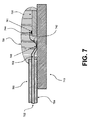
- FIG. 7 shows a third embodiment of the direct and permanent connection of a signal wire of the cable connection to a contact of an integrated cable module circuit, in accordance with certain aspects of the invention.
- FIG. 8 shows a forth embodiment of a direct and permanent connection of a signal wire of the cable connection to a contact of a packed integrated cable module circuit, in accordance with certain aspects of the invention.
- FIG. 3 shows a schematic block diagram of the active bidirectional cable connection according to the proposed configuration principle of the present invention.
- the wire conducted data connection 300 is comprised of two coaxial cables 301 , 302 as a differential wire pair.
- the coaxial cables 301 , 302 are directly and permanent connected to respective cable modules 310 , 320 .
- the respective cable modules 310 , 320 at each end of the wire conducted data connection 300 may comprise at least the required circuit 311 , 321 for transmitting and sending data over the differential wire pair formed by the two coaxial cables 301 , 302 .
- the cable modules 310 , 320 may comprise respective signal driver 313 , 323 for supplying a signal to be sent to the other end of the wire conducted data connection 300 .
- the cable modules 310 , 320 may comprise respective receiving comparators 315 , 325 , which are adapted for detecting a signal, send via the wire conducted data connection 300 from the cable module at the other end.
- the combination of the respective signal drivers 313 , 323 and receiving compactors 315 , 325 form respective transceiver units integrated in the respective cable modules 310 , 320 .
- connection means 317 , 327 may involve conventional interconnection methods and designs, such as those known from surface mounted electronic components as well as packed integrated circuits. In these cases, the cable connection may be mounted on the respective PCB parts of the electronic device to be interconnected.
- connection means 317 , 327 it is also possible have connectors as connection means 317 , 327 .
- One such example is depicted in FIG. 3 by reference signs 318 and 319 for cable module 310 as well as by reference signs 328 and 329 for cable module 320 , where reference signs 318 , 319 and 328 , 329 represent respective miniaturized connector pairs, which are available in different types.
- this cable interconnection relates to electrically and mechanically connecting the respective used wire or cable type directly and permanent to the respective integrated circuit cable of the respective module 310 , 320 .
- the inner conductor wire and the outer conductor can be bonded to respective connection pads provided at the integrated circuit of the respective cable modules, which may serve as an integrated interface in/to the cable interconnection.
- FIGS. 4 a and 4 b in which an illustrative use case/application for a wire conducted data connection or cable interconnection is shown.
- FIG. 4 a shows an illustration of a mobile terminal or mobile phone 400 (or mobile for short), which is comprised of two parts 410 , 420 .
- FIG. 4 a includes an indication of the phone's size by reference sign 405 pointing to an arrow, which may be in closed conduction about 7 cm. This indication 405 may be helpful for understanding the cable length of cable connection 450 discussed below in connection with FIG. 4 b .
- An upper part 410 contains, e.g., a small number of keys 412 and a display 414
- the lower part 420 contains, e.g., a keypad 422 with several conventional keys typically known in the area of phones.
- the two parts 410 , 420 are mechanically connected together by means of a sliding mechanism, such phones are therefore also known as “slider phones”.
- the mechanical aspects of the connection will not be focused here in more detail.
- phones having two or more parts or components which are arranged moveable to each other may require large numbers of lanes in the electrical interconnection(s), which may result in the discussed electronic disadvantages as well as the high mechanical stresses during the life time of the phone.
- FIG. 4 b a illustrative data connection is shown between two parts 410 , 420 of the mobile device shown in FIG. 4 a .
- the data connection in FIG. 4 b connects respective printed circuit boards (PCB), modules 410 *, 420 * with electronic circuit which are in each respective part of the mobile phone.
- the electronic circuit and components on the modules 410 * and 420 * may comprise a multi-point bus, comprising portions 431 , 432 to which respective functional components 441 , 442 are physically connected together by respective signal wires.
- the cable connection 450 may be comprised of a single coaxial cable 451 that provides for simultaneous bidirectional signaling.
- the electronic interconnection may provide for a reliable electronic interface between two functional parts of the phone, the modules 410 *, 420 *. Additionally, due to its robust configuration, the cable connection may be able to better withstand the mechanical stress from use during the expected/desired lifetime of the product.
- the cable connection may provide an active high-speed bidirectional interconnection for data exchange between the modules 410 * and 420 *.
- a respective cable module 452 , 454 (each of which may comprise the respective integrated cable module circuit) which may be directly and permanent connected to the coaxial cable 451 .
- the cable manufacturer may manufacture the cable connection 450 as a unit. That is to say, the coaxial cable may be assembled together with the cable modules 452 , 454 at each end.
- the cable assembly may be made from a single coaxial cable.
- the outer conductor of the coaxial cable may be made thick enough to provide enough shielding for a single-ended signal transmission.
- the coaxial cable outer conductor can be connected to transceiver ground in the cable modules 4521 , 454 , in a way which may provide for low inductance (low transfer impedance) so that single-ended signaling in the range of Gb/s rates may be possible.
- such a single coaxial cable may be able to replace optical fiber connections, such as those conventionally used in certain mobile devices.
- single-cable signaling may require that the M-PHY, under specification in MIPI, will be ready.
- certain embodiments may use the well-controlled interconnection described herein to allow for similar bit rates as conventional optical signaling techniques.
- normal low-speed CMOS signaling may potentially be made easier and more power efficient in comparison to optics.
- a single coaxial cable may be flexible enough to tolerate rotation and bending.
- the connection may also be an external cable connection, such as a connection between a mobile device and a “headset” with, for example, near-eye display.
- FIG. 5 to 8 several embodiments of the direct and permanent connection of at least one signal wire of a cable connection to a respective cable module circuit are shown.
- the following discussion and descriptions of these embodiments are not intended as limitations of the invention, since many details and/or aspects of a certain embodiment may be combined in further embodiments which are not shown or described herein.
- FIG. 5 an embodiment of the direct and permanent cable connection is illustrated, in which for the cable a coaxial cable 500 is used.
- the coaxial cable 500 comprises an inner conductor 502 , which is used as the signal wire 503 , and an outer conductor 504 , which may be used for shielding proposes.
- the coaxial cable 500 may be fixed to a printed circuit board (PCB) 510 , which may be the circuit board to which the cable connection is to be established.
- PCB 510 there may be at least one through-hole 512 , to which the coaxial cable 500 is fixed.
- the fixation may be implemented by soldering the outer conductor 504 to conductor material of the PCB 510 at the through-hole 512 , the diameter of which is indicated by the arrow 514 and may be designed to correspond substantially to the outer diameter of the cable 500 . Accordingly, by this configuration the outer conductor 504 can be connected to ground potential of the circuit on the PCB 510 .
- the direct and permanent connection of the signal wire 503 to a contact of a cable module circuit 520 is arranged in a flip chip arrangement.
- the signal wire 503 of the cable 500 is directly connected to the respective contact of the integrated cable module circuit 520 by means of a signal bump 522 .
- the ground contact of the integrated cable module device 520 may be connected via a respective ground bump 524 to a ground conductor 514 of the PCB 510 , which may also be connected with outer conductor 504 of the cable 500 .
- the whole arrangement may finally be covered by a molded resin, an epoxy, or suitable plastic material, in order to provide for protection and additional support (not shown in FIG. 5 ).
- a coaxial cable 600 is once again used.
- the coaxial cable 600 comprises the inner conductor 602 used as the signal wire 603 and the outer conductor 604 , which may be used for shielding proposes.
- the coaxial cable 600 may be fixed on top of a printed circuit board (PCB) 610 , which is, for example, one of the circuit boards of FIG. 4 b , to which the cable connection may be established.
- PCB printed circuit board
- the integrated cable module circuit 620 may be similar to the one described with FIG. 5 .
- the chip or die with the integrated cable module circuit may be arranged in a flip chip configuration as shown, and the required electrical contacts may be again provided by respective bumps (e.g., a signal bump 622 for connection with the signal wire 603 and a ground bump 624 for supply of a ground potential to the cable module IC).
- the direct and permanent connection of the signal wire 603 and the signal bump 622 may be established at the same time, for example, when the integrated cable module circuit 620 (cable module IC) is surface mounted in its turned over orientation on the PCB 610 .
- a direct and permanent connection between the signal wire 603 and the input and/or output of the integrated cable module circuit 620 may provide the properties required for good signal transmission. Additionally, the whole arrangement is protected by a cover 630 (for example, of a molded resin or an epoxy material) for shielding and protecting the connections, and for additional fixation of the cable 600 .
- a cover 630 for example, of a molded resin or an epoxy material
- FIG. 7 a third embodiment is shown illustrating a direct and permanent cable connection in which a coaxial cable 700 is used.
- the inner conductor 702 (signal wire 730 ) and the outer conductor 704 of the coaxial cable 700 are attached/fixed to the printed circuit board (PCB) 710 .
- the PCB 710 the chip or die with integrated cable module circuit 720 may be placed in a conventional manner with the contacts in upside orientation with respect to the upper side of the PCB 720 .
- a contact pad 740 to which the signal wire 703 of the coaxial cable 700 is connected, for example, by soldering or ultrasonic/laser bonding.
- the direct and permanent connection between the signal wire 703 and a contact pad 741 at the integrated cable module circuit 720 may be established by a bonding wire 742 .
- the whole arrangement is protected by a cover 730 of molded resin or an epoxy material for shielding and protection of the connections, as well as for additional fixation of the cable 700 .
- the coaxial cable 800 may comprise an inner conductor 802 used as the signal wire 803 , and an outer conductor 804 shielding the signal wire 803 .
- the coaxial cable 800 may be attached/fixed to a printed circuit board (PCB) 810 , on which a SOIC packed cable module circuit 820 may be mounted in a through-hole mounting manner.
- PCB 810 there may be a required number of through-holes corresponding to the number of pins of the SOIC packed cable module circuit 820 .
- a further fixation of the cable 800 may be made by soldering of the outer conductor 804 to a conductor material of the PCB 810 . Accordingly, the outer conductor 804 may be connected to ground potential of the circuit on the PCB 810 for better shielding.
- the signal wire 803 is permanently connected to a contact of a small outline integrated circuit (SOIC) packed cable module circuit 820 (e.g., packed into an SOIC packaging).
- SOIC small outline integrated circuit
- the signal wire 803 of the cable 800 is directly and permanently connected to the respective contact of the SOIC cable module 820 by means of a signal contact pin 822 .
- the interconnection of the signal wire 803 to the SOIC cable module 820 may be covered by a molded resin, an epoxy, or suitable plastic material, in order to provide for protection and additional support.
- the cable 800 may be attached or fixed to the opposite side of the PCB 810 .
- the connection of the signal wire(s) 803 may be established on the cable side of the PCB 810 .
- the signal wire of the cable 800 may be inserted into the respective through-hole of the PCB 810 (e.g., similarly to FIG. 5 ), and connected by soldering or any other suitable method or process to the respective pin of the packed integrated cable module circuit 820 .
- the integrated cable module circuit is packed in a “conventional” IC packaging, such as a SOJ or SOIC packaging.
- a SOJ or SOIC packaging As described above the chip with the integrated cable module circuit can be arranged in an up-side orientation within a lead frame, which provides required contact pads for interconnection. That is to say, the module circuit may be interconnected with the lead frame pads, for example, by bonding wires. This situation corresponds roughly the embodiment described in FIG. 7 , in which the contact pad 740 is located on the lead frame.
- the signal wire may be connected to a contact pad of the lead frame by a suitable permanent method, such as ultrasonic or laser bonding.
- a suitable permanent method such as ultrasonic or laser bonding.
- this arrangement of the coaxial cable connected by its signal wire to the dedicated contact pad of the lead frame together with the respective integrated cable module circuit may be packaged by a suitable material (e.g., plastics or other moldable material) for IC packaging.
- a suitable material e.g., plastics or other moldable material
- the entire cable connection may come as one entity or cable connection unit comprising two standardizable IC packages, for example SOIC packages, which may be interconnected by the cable, such as a suitable coaxial cable. Then, this cable connection unit may simply be mounted to the printed circuit boards of an electronic device by the device manufacturer. In this example and similar embodiments, the distance of the direct and permanent connection of a signal wire in/into the integrated cable module circuit may be further reduced.
- Certain embodiments may use a high-quality coaxial cable (or a pair of coaxial cables) for the cable connection, so that external interference may be reduced, and to increase the accuracy of the impedance tolerance matching between the transceiver and the cable.
- a good-quality coaxial cable may have a thick outer conductor that may attenuate ESD pulses so that only a limited ESD protection might be needed on the transceiver side. By implementation of only limited ESD protection (which is necessary during manufacturing) on the transceivers capacitive load at the transceiver may be further reduced.
- “High-quality” or “good-quality” coaxial cable may refer to a cable that provides tight impedance tolerances, for example 2% to 5%, low dielectric losses, for example loss tangent (synonym for dissipation factor) of at least 0.002.
- the thick outer connector for shielding may be composed of a metal foil and braided mesh wire instead of very thin moralized polyethylene foil.
- the transceivers may be made using modern semiconductor technology and manufacturing processes, which may result in relatively accurate tolerances.
- Modern semiconductor technology may refer to CMOS technology less than or equal to 65 nm (e.g., even as low as 45 nm CMOS or lower).
- RTD resonance tunnel diode
- signal wires of the coaxial cable(s) may be connected directly to silicon (chip/die) of the transceiver circuits, so that package and connector impedance discontinuations may be further avoided.
- the connection between cable conductors and the integrated cable module circuit part may form a sealed single component.
- the output capacitance of the driver circuits of the integrated cable module circuit may be reduced, for example, by using NMOS pull-up and pull-down transistors as driving elements instead of PMOS pull-up transistor. Additionally, resistive pull-up and NMOS pull-down transistors may provide for small output capacitance.
- the serial link may comprise an embedded clocking.
- An example for an application of this kind of link may be MIPI's M-PHY.
- Such implementations may have additional advantages in applications/products where an optical fiber connection may be used, for example, through the hinge connecting two parts of the phone.
- bidirectional 1-cable solution in electronic devices using several wires/cables in an interconnection, an embodiment involving a bidirectional 1-cable solution can be applied to enable further miniaturization of connection mechanics (e.g. hinges) between the moving parts of the electronic devices.
- bidirectional 1-cables might also be used when the number of signal wires should be reduced or should be small.
- certain embodiments relate to a cable connection with at least one cable as a wire conducted signal interconnection between two cable module circuits connected to respective ends of the cable connection.
- Cable conductors may be directly and permanently electrically connected at each end to contacts at a cable module circuit.
- the cable module circuits may be arranged for sending and/or receiving of a wire-conducted signal transmitted via the cable connection.
- the cable module circuits can be matched to the cable impedance with high accuracy.
- the connection may be protected from other kinds of disturbances.
- high simultaneous bidirectional bit rates may potentially be possible using this kind of interconnection between electronic units or modules.
- the present invention is not restricted to the embodiment described above, but can be implemented in any circuit where at least two functional portions of circuit which require a high-speed data connection are to be connected by means of a wire conducted interconnection.
- this cable connection design may be a cost-effective solution for mobile devices that send signals through a flexible mechanical structure such as a hinge.
- many modern mobile electronic devices such as mobile phones, laptops, personal digital assistants or alike, may use one or more embodiments of the disclosed cable connection design.
Landscapes
- Engineering & Computer Science (AREA)
- Microelectronics & Electronic Packaging (AREA)
- Details Of Connecting Devices For Male And Female Coupling (AREA)
Abstract
Description
Claims (18)
Priority Applications (1)
| Application Number | Priority Date | Filing Date | Title |
|---|---|---|---|
| PCT/IB2007/002330 WO2008032150A2 (en) | 2006-09-15 | 2007-08-13 | Simultaneous bidirectional cable interface |
Applications Claiming Priority (3)
| Application Number | Priority Date | Filing Date | Title |
|---|---|---|---|
| EP06019369 | 2006-09-15 | ||
| EP06019369 | 2006-09-15 | ||
| EP06019369.5 | 2006-09-15 |
Publications (2)
| Publication Number | Publication Date |
|---|---|
| US20080067637A1 US20080067637A1 (en) | 2008-03-20 |
| US7803017B2 true US7803017B2 (en) | 2010-09-28 |
Family
ID=39187707
Family Applications (1)
| Application Number | Title | Priority Date | Filing Date |
|---|---|---|---|
| US11/653,929 Expired - Fee Related US7803017B2 (en) | 2006-09-15 | 2007-01-17 | Simultaneous bidirectional cable interface |
Country Status (1)
| Country | Link |
|---|---|
| US (1) | US7803017B2 (en) |
Cited By (3)
| Publication number | Priority date | Publication date | Assignee | Title |
|---|---|---|---|---|
| CN102843859A (en) * | 2012-08-14 | 2012-12-26 | 广东欧珀移动通信有限公司 | Short connection method and printed circuit board (PCB) pad package for different networks |
| US9202789B2 (en) | 2014-04-16 | 2015-12-01 | Qualcomm Incorporated | Die package comprising die-to-wire connector and a wire-to-die connector configured to couple to a die package |
| US20220069502A1 (en) * | 2020-09-02 | 2022-03-03 | Avx Corporation | Electrical Connector |
Families Citing this family (7)
| Publication number | Priority date | Publication date | Assignee | Title |
|---|---|---|---|---|
| JP2010535453A (en) * | 2007-08-02 | 2010-11-18 | フェアチャイルド セミコンダクター コーポレイション | Method and circuit for interleaving and serializing / deserializing LCD, camera, keypad and GPIO data via serial stream |
| JP5653610B2 (en) * | 2009-12-02 | 2015-01-14 | オリンパス株式会社 | Electronic circuit module and coaxial cable connection method |
| EP2391042B1 (en) * | 2010-05-27 | 2015-07-29 | Telefonaktiebolaget L M Ericsson (publ) | Efficient error handling on a link using ARQ and multiple NACKs associated with multiple error thresholds |
| WO2011155975A2 (en) * | 2010-06-08 | 2011-12-15 | R&D Circuit, Inc. | Method and structure for directly connecting coaxial or micro coaxial cables to the interior side of pads of a printed circuit baord to improve signal integrity of an electrical circuit |
| WO2016039740A1 (en) * | 2014-09-10 | 2016-03-17 | Northrop Grumman Systems Corporation | Ground grid for superconducting circuits |
| JP7003478B2 (en) * | 2017-08-02 | 2022-01-20 | オムロン株式会社 | Electronic device and its manufacturing method |
| CN112563782A (en) * | 2019-09-25 | 2021-03-26 | 连展科技电子(昆山)有限公司 | Double-row welding wire structure |
Citations (7)
| Publication number | Priority date | Publication date | Assignee | Title |
|---|---|---|---|---|
| JPS62119949A (en) | 1985-11-19 | 1987-06-01 | Nec Corp | Package for semiconductor device |
| US4856023A (en) * | 1986-07-23 | 1989-08-08 | Ncr Corporation | System for maintaining low bit error rate in a starcoupled network of direct coupled stations |
| JP2000035775A (en) | 1998-07-17 | 2000-02-02 | Nok Corp | Electrophoresis display device |
| US20020137476A1 (en) | 2001-03-22 | 2002-09-26 | Shin Ji Seop | Slide type mobile phone using slide module |
| US20020153977A1 (en) | 2001-04-16 | 2002-10-24 | Mcdonough Robert J. | Apparatus and method for angled coaxial to planar structure broadband transition |
| US20040245610A1 (en) * | 2003-06-04 | 2004-12-09 | Dong Zhong | Flex tape architecture for integrated circuit signal ingress/egress |
| US20050200413A1 (en) | 2004-03-12 | 2005-09-15 | Keitaro Fujimori | Flexible substrate and electronic equipment |
-
2007
- 2007-01-17 US US11/653,929 patent/US7803017B2/en not_active Expired - Fee Related
Patent Citations (7)
| Publication number | Priority date | Publication date | Assignee | Title |
|---|---|---|---|---|
| JPS62119949A (en) | 1985-11-19 | 1987-06-01 | Nec Corp | Package for semiconductor device |
| US4856023A (en) * | 1986-07-23 | 1989-08-08 | Ncr Corporation | System for maintaining low bit error rate in a starcoupled network of direct coupled stations |
| JP2000035775A (en) | 1998-07-17 | 2000-02-02 | Nok Corp | Electrophoresis display device |
| US20020137476A1 (en) | 2001-03-22 | 2002-09-26 | Shin Ji Seop | Slide type mobile phone using slide module |
| US20020153977A1 (en) | 2001-04-16 | 2002-10-24 | Mcdonough Robert J. | Apparatus and method for angled coaxial to planar structure broadband transition |
| US20040245610A1 (en) * | 2003-06-04 | 2004-12-09 | Dong Zhong | Flex tape architecture for integrated circuit signal ingress/egress |
| US20050200413A1 (en) | 2004-03-12 | 2005-09-15 | Keitaro Fujimori | Flexible substrate and electronic equipment |
Non-Patent Citations (5)
| Title |
|---|
| Casper B et al., "An 8-Gb/s Simultaneous Bidirectional Link with on-die Waveform Capture" IEEE Journal of Solid-State Circuits, IEEE Service Center, vol. 38, No. 12, Dec. 2003, pp. 2111-2120 XP011104339. |
| Evelina Yeung and Mark A. Horowitz, "A 2.4 Gb/s/pin Simultaneous Bidirectional Parallel Link with Perpin Skew Compensation", IEEE Journal of Solid-State Circuits, vol. 35, No. 11, Nov. 2000, pp. 1619. |
| PCT International Search Report, PCT/IB2007/002330, maildate Aug. 5, 2008. |
| Robert Drost, "Architecture and Design of a Simultaneously Bidirectional Single-ended High Speed Chip-to-Chip Interface", SMLI TR-2002-107, Feb. 2002. |
| Toshiro Takahashi et al., "110-GB/s Simultaneous Bidirectional Transceiver Logic Synchronized with a System Clock" IEEE Journal of Solid-State Circuits, IEEE Service Center, vol. 34, No. 11, Nov. 1999, p. 1526, 1527 and p. 1530. |
Cited By (3)
| Publication number | Priority date | Publication date | Assignee | Title |
|---|---|---|---|---|
| CN102843859A (en) * | 2012-08-14 | 2012-12-26 | 广东欧珀移动通信有限公司 | Short connection method and printed circuit board (PCB) pad package for different networks |
| US9202789B2 (en) | 2014-04-16 | 2015-12-01 | Qualcomm Incorporated | Die package comprising die-to-wire connector and a wire-to-die connector configured to couple to a die package |
| US20220069502A1 (en) * | 2020-09-02 | 2022-03-03 | Avx Corporation | Electrical Connector |
Also Published As
| Publication number | Publication date |
|---|---|
| US20080067637A1 (en) | 2008-03-20 |
Similar Documents
| Publication | Publication Date | Title |
|---|---|---|
| US7803017B2 (en) | Simultaneous bidirectional cable interface | |
| US9647715B2 (en) | Contactless signal splicing using an extremely high frequency (EHF) communication link | |
| KR100721320B1 (en) | A connection module for integrated circuit device and integrated circuit device adapted therefor | |
| JP3803596B2 (en) | Package type semiconductor device | |
| US20190051587A1 (en) | Ic package | |
| US7818878B2 (en) | Integrated circuit device mounting with folded substrate and interposer | |
| US20060091507A1 (en) | IC package structures having separate circuit interconnection structures and assemblies constructed thereof | |
| US20040091719A1 (en) | Layered board, and apparatus incorporation such layered board | |
| US20060035510A1 (en) | LSI package having interface function with exterior, circuit device including the same, and manufacturing method of circuit device | |
| US11011886B2 (en) | Packaging of a directly modulated laser chip in photonics module | |
| WO2008032150A2 (en) | Simultaneous bidirectional cable interface | |
| US20090129786A1 (en) | Coupling of optical interconnect with electrical device | |
| US20090152689A1 (en) | Integrated Circuit Package for High-Speed Signals | |
| US7372139B2 (en) | Semiconductor chip package | |
| US20110294308A1 (en) | Substrate and ic socket | |
| US10090993B2 (en) | Packaged circuit | |
| JP2006053266A (en) | Optical semiconductor module and semiconductor apparatus using the same | |
| US10709013B2 (en) | Multilayer wiring board and differential transmission module | |
| US7863716B2 (en) | Method and apparatus of power ring positioning to minimize crosstalk | |
| Jaussi et al. | Multi-Gbit I/O and interconnect co-design for power efficient links | |
| JP2001044452A (en) | Optical communication module | |
| TW202210885A (en) | Hybrid multi-layered optical flexible printed circuit device and manufacturing method thereof | |
| US10685942B2 (en) | Reflection-canceling package trace design | |
| US7304863B1 (en) | Integrated circuit including external electronic components with low insertion loss | |
| JP3597830B2 (en) | Electronic circuit device, electronic device package, and transmission line termination method |
Legal Events
| Date | Code | Title | Description |
|---|---|---|---|
| AS | Assignment |
Owner name: NOKIA CORPORATION, FINLAND Free format text: ASSIGNMENT OF ASSIGNORS INTEREST;ASSIGNOR:VOUTILAINEN, MARTTI;REEL/FRAME:018800/0313 Effective date: 20061218 |
|
| FEPP | Fee payment procedure |
Free format text: PAYOR NUMBER ASSIGNED (ORIGINAL EVENT CODE: ASPN); ENTITY STATUS OF PATENT OWNER: LARGE ENTITY |
|
| STCF | Information on status: patent grant |
Free format text: PATENTED CASE |
|
| FPAY | Fee payment |
Year of fee payment: 4 |
|
| AS | Assignment |
Owner name: NOKIA TECHNOLOGIES OY, FINLAND Free format text: ASSIGNMENT OF ASSIGNORS INTEREST;ASSIGNOR:NOKIA CORPORATION;REEL/FRAME:035561/0501 Effective date: 20150116 |
|
| MAFP | Maintenance fee payment |
Free format text: PAYMENT OF MAINTENANCE FEE, 8TH YEAR, LARGE ENTITY (ORIGINAL EVENT CODE: M1552) Year of fee payment: 8 |
|
| FEPP | Fee payment procedure |
Free format text: MAINTENANCE FEE REMINDER MAILED (ORIGINAL EVENT CODE: REM.); ENTITY STATUS OF PATENT OWNER: LARGE ENTITY |
|
| LAPS | Lapse for failure to pay maintenance fees |
Free format text: PATENT EXPIRED FOR FAILURE TO PAY MAINTENANCE FEES (ORIGINAL EVENT CODE: EXP.); ENTITY STATUS OF PATENT OWNER: LARGE ENTITY |
|
| STCH | Information on status: patent discontinuation |
Free format text: PATENT EXPIRED DUE TO NONPAYMENT OF MAINTENANCE FEES UNDER 37 CFR 1.362 |
|
| FP | Lapsed due to failure to pay maintenance fee |
Effective date: 20220928 |