US7800424B2 - Apparatus for supplying overdriving signal - Google Patents
Apparatus for supplying overdriving signal Download PDFInfo
- Publication number
- US7800424B2 US7800424B2 US11/958,277 US95827707A US7800424B2 US 7800424 B2 US7800424 B2 US 7800424B2 US 95827707 A US95827707 A US 95827707A US 7800424 B2 US7800424 B2 US 7800424B2
- Authority
- US
- United States
- Prior art keywords
- signal
- overdriving
- voltage
- signals
- supplying
- Prior art date
- Legal status (The legal status is an assumption and is not a legal conclusion. Google has not performed a legal analysis and makes no representation as to the accuracy of the status listed.)
- Expired - Fee Related
Links
Images


Classifications
-
- G—PHYSICS
- G11—INFORMATION STORAGE
- G11C—STATIC STORES
- G11C7/00—Arrangements for writing information into, or reading information out from, a digital store
- G11C7/06—Sense amplifiers; Associated circuits, e.g. timing or triggering circuits
- G11C7/08—Control thereof
-
- G—PHYSICS
- G11—INFORMATION STORAGE
- G11C—STATIC STORES
- G11C11/00—Digital stores characterised by the use of particular electric or magnetic storage elements; Storage elements therefor
- G11C11/21—Digital stores characterised by the use of particular electric or magnetic storage elements; Storage elements therefor using electric elements
- G11C11/34—Digital stores characterised by the use of particular electric or magnetic storage elements; Storage elements therefor using electric elements using semiconductor devices
- G11C11/40—Digital stores characterised by the use of particular electric or magnetic storage elements; Storage elements therefor using electric elements using semiconductor devices using transistors
- G11C11/401—Digital stores characterised by the use of particular electric or magnetic storage elements; Storage elements therefor using electric elements using semiconductor devices using transistors forming cells needing refreshing or charge regeneration, i.e. dynamic cells
- G11C11/4063—Auxiliary circuits, e.g. for addressing, decoding, driving, writing, sensing or timing
- G11C11/407—Auxiliary circuits, e.g. for addressing, decoding, driving, writing, sensing or timing for memory cells of the field-effect type
- G11C11/4076—Timing circuits
-
- G—PHYSICS
- G11—INFORMATION STORAGE
- G11C—STATIC STORES
- G11C11/00—Digital stores characterised by the use of particular electric or magnetic storage elements; Storage elements therefor
- G11C11/21—Digital stores characterised by the use of particular electric or magnetic storage elements; Storage elements therefor using electric elements
- G11C11/34—Digital stores characterised by the use of particular electric or magnetic storage elements; Storage elements therefor using electric elements using semiconductor devices
- G11C11/40—Digital stores characterised by the use of particular electric or magnetic storage elements; Storage elements therefor using electric elements using semiconductor devices using transistors
- G11C11/401—Digital stores characterised by the use of particular electric or magnetic storage elements; Storage elements therefor using electric elements using semiconductor devices using transistors forming cells needing refreshing or charge regeneration, i.e. dynamic cells
- G11C11/4063—Auxiliary circuits, e.g. for addressing, decoding, driving, writing, sensing or timing
- G11C11/407—Auxiliary circuits, e.g. for addressing, decoding, driving, writing, sensing or timing for memory cells of the field-effect type
- G11C11/409—Read-write [R-W] circuits
- G11C11/4091—Sense or sense/refresh amplifiers, or associated sense circuitry, e.g. for coupled bit-line precharging, equalising or isolating
-
- G—PHYSICS
- G11—INFORMATION STORAGE
- G11C—STATIC STORES
- G11C5/00—Details of stores covered by group G11C11/00
- G11C5/14—Power supply arrangements, e.g. power down, chip selection or deselection, layout of wirings or power grids, or multiple supply levels
- G11C5/143—Detection of memory cassette insertion or removal; Continuity checks of supply or ground lines; Detection of supply variations, interruptions or levels ; Switching between alternative supplies
-
- G—PHYSICS
- G11—INFORMATION STORAGE
- G11C—STATIC STORES
- G11C5/00—Details of stores covered by group G11C11/00
- G11C5/14—Power supply arrangements, e.g. power down, chip selection or deselection, layout of wirings or power grids, or multiple supply levels
- G11C5/145—Applications of charge pumps; Boosted voltage circuits; Clamp circuits therefor
-
- G—PHYSICS
- G11—INFORMATION STORAGE
- G11C—STATIC STORES
- G11C7/00—Arrangements for writing information into, or reading information out from, a digital store
- G11C7/22—Read-write [R-W] timing or clocking circuits; Read-write [R-W] control signal generators or management
-
- G—PHYSICS
- G11—INFORMATION STORAGE
- G11C—STATIC STORES
- G11C2207/00—Indexing scheme relating to arrangements for writing information into, or reading information out from, a digital store
- G11C2207/06—Sense amplifier related aspects
- G11C2207/065—Sense amplifier drivers
Definitions
- the embodiments described herein relate to a semiconductor integrated circuit, and more particularly, to an apparatus for supplying an overdriving signal in a semiconductor integrated circuit.
- DRAM Dynamic Random Access Memory
- DRAM Dynamic Random Access Memory
- VT threshold voltage
- an overdriving scheme where the sense amplifier receives a voltage Vcore as a driving voltage, and an external voltage VDD as an overdriving voltage.
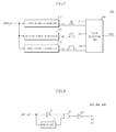
- a conventional overdriving signal supplying apparatus includes first to third NMOS transistors NM 1 , NM 2 , and NM 3 , a sense amplifier 2000 , and a pre-charging unit 3000 .
- the first to third NMOS transistors NM 1 to NM 3 respectively receive first to third sense amplifier control signals (SAP 1 ), (SAP 2 ), and (SAN) and supply to the sense amplifier 2000 the external voltage VDD, the core voltage Vcore, and a ground voltage VSS, respectively.
- the precharging unit 3000 supplies a pre-charge voltage Vblp to the sense amplifier 2000 in a precharge mode.
- the overdriving signal supplying apparatus when a word line WL is enabled and then the third sense amplifier control signal (SAN) is enabled, the ground voltage VSS is supplied to the sense amplifier 2000 . Then, the first sense amplifier control signal (SAP 1 ) is enabled for a predetermined time to overdrive sense amplifier 2000 , causing the external voltage VDD to be supplied to the sense amplifier 2000 . Therefore, amplification by the sense amplifier 2000 can be rapidly performed. Subsequently, the second sense amplifier control signal (SAP 2 ) is enabled, and the first sense amplifier control signal (SAP 1 ) is disabled, so that the core voltage Vcore is supplied to the sense amplifier 2000 . In this way, a pair of bit lines of the sense amplifier 2000 reach the core voltage Vcore and the ground voltage VSS, respectively.
- the threshold voltage and current of transistors included in the sense amplifier 2000 change according to the external voltage VDD. Therefore, when the external voltage VDD is low, the overdriving voltage may be low, and when the external voltage VDD is high, excessive overdriving may occur. As a result, when the overdriving voltage is lower, a sensing margin of the sense amplifier 2000 is reduced, which may cause a malfunction. Simply increasing the overdriving voltage can cause the sensitivity of the sense amplifier 2000 to be lowered and power consumption to increase. Also, when the external voltage VDD exhibits significant noise, the reliability and sensitivity of a sense amplifier are considerably lowered.
- an apparatus for supplying an overdriving signal includes a voltage detecting block that outputs a plurality of detection signals according to the level of an external voltage, and a pulse generator that outputs the overdriving signals having different pulse widths in response to the plurality of detection signals.
- an apparatus for supplying an overdriving signal includes a voltage detecting block that detects the level of an external voltage, defines sections of the external voltage, and outputs a plurality of detection signals that are activated or inactivated in a specific voltage section and a pulse generator that outputs the overdriving signals of different pulse widths corresponding to the plurality of detection signals that are generated according to the detected level of the external voltage.
- an apparatus for supplying an overdriving signal includes a voltage detecting block including a plurality of detectors each of which compares a reference voltage with a divided voltage that is proportional to a detected external voltage and outputs a detection signal corresponding to the result of the comparison and a pulse generator that outputs the overdriving signals of different pulse widths corresponding to the plurality of detection signals that are generated according to the level of the detected external voltage.
- the pulse generator includes a plurality of signal generators that generate pulses of different widths, the number of pulses corresponding to the number of detection signals and a pulse selecting unit that selects one of the output signals of the plurality of signal generators in response to the detection signals, and outputs the selected signal as the overdriving signal.
- FIG. 1 is a block diagram illustrating an exemplary semiconductor memory apparatus that includes an overdriving scheme including a sense amplifier;
- FIG. 2 is a waveform diagram illustrating the operation of the sense amplifier shown in FIG. 1 ;
- FIG. 3 is a block diagram illustrating an apparatus for supplying an overdriving signal according to one embodiment
- FIG. 4 is a block diagram illustrating a voltage detecting block that can be included in the apparatus illustrated in FIG. 3 ;
- FIG. 5 is a detailed circuit diagram illustrating first voltage detector that can be included in the block illustrated in FIG. 4 ;
- FIG. 6 is a block diagram illustrating an alternative embodiment of a voltage detecting block that can be included in the apparatus illustrated in FIG. 3 ;
- FIG. 7 is a block diagram illustrating a pulse generator that can be included in the apparatus illustrated in FIG. 3 ;
- FIG. 8 is a detailed circuit diagram illustrating the first, second and third signal generators that can be included in the pulse generator illustrated in FIG. 7 ;
- FIG. 9 is a block diagram illustrating a pulse selecting unit that can be included in the pulse generator illustrated in FIG. 7 ;
- FIG. 10 is a detailed circuit diagram illustrating a control unit that can be included in the pulse selecting unit illustrated in FIG. 9 ;
- FIG. 11 is a detailed circuit diagram illustrating a transmitting unit that can be included in the pulse selecting unit illustrated in FIG. 9 .
- FIG. 3 is a diagram illustrating a overdriving signal supplying apparatus 101 configured in accordance with one embodiment.
- the overdriving signal supplying apparatus 101 can include a voltage detecting block 100 and a pulse generator 200 .
- the voltage detecting block 100 can be configured to generate a plurality of detection signals D 1 , D 2 , . . . and Dn (where n is an integer number) according to the level of an external voltage VDD.
- the voltage detecting block 100 can be implemented as a general level detector circuit, depending on the embodiment.
- the pulse generator 200 can be configured to generate signals having different pulse widths according to the plurality of detection signals D 1 , D 2 , . . . , and Dn, and to output.
- the overdriving signal supplying apparatus 101 shown in FIG. 3 can be configured to generate a first sense amplifier control signals (SAP 1 ) having different pulse widths according to the level of the external voltage VDD. More specifically, when the external voltage VDD is low, the overdriving signal supplying apparatus 101 can be configured to generate the first sense amplifier control signal (SAP 1 ) having a large pulse width. On the other hand, when the external voltage VDD is high, the overdriving signal supplying apparatus 101 can be configured to generate the first sense amplifier control signal (SAP 1 ) having a small pulse width. In this way, it is possible to solve the problem of slow sensing and amplifying operations when the external voltage VDD is low and the problem of excessive sensing and amplifying operations when the external voltage VDD is high, which results in an increase in sensing margin.
- FIG. 4 is a diagram illustrating a voltage detecting block 100 in more detail.
- the voltage detecting block 100 can include a first to third voltage detectors 110 , 120 , and 130 . Three voltage detectors are illustrated for the convenience of explanation, but the invention is not limited thereto.
- the first to third voltage detectors 110 , 120 , and 130 can be configured to compare a reference voltage VREF with first to third divided voltages DET 1 , DET 2 , and DET 3 , respectively. In this way, the first to third voltage detectors 110 , 120 , and 130 can generate detection signals D 1 , D 2 , and D 3 according to the results of the comparison.
- the first to third divided voltages DET 1 , DET 2 , and DET 3 can have sequentially higher voltage levels, while the external voltage VDD has a constant level. Therefore, the first to third detection signals D 1 , D 2 , and D 3 , which are output signals of the first to third voltage detectors 110 , 120 , and 130 , can have different values according to the level of the external voltage VDD.
- the first voltage detector 110 can include a voltage dividing unit 112 , a current supply unit 111 , a current passing unit 114 , a comparator 113 , and an output buffering unit 115 .
- the voltage dividing unit 112 can divide the external voltage VDD to generate a first divided voltage DET 1 .
- the voltage dividing unit 112 can, e.g., include a first resistor R 1 and a second resistor R 2 connected in series to each other. The first resistor R 1 and the second resistor R 2 divide the external voltage VDD to generate the first divided voltage DET 1 .
- the comparator 113 can, e.g., includes first and second NMOS transistors NM 1 and NM 2 .
- the first NMOS transistor NM 1 has a gate to which the first divided voltage DET 1 is applied, a drain connected to the current supply unit 111 , and a source connected to the current passing unit 114 .
- the second NMOS transistor NM 2 has a gate to which the reference voltage VREF is applied, a drain connected to the current supply unit 111 , and a source connected to the current passing unit 114 .
- the current supply unit 111 can, e.g., include first and second PMOS transistors PM 1 and PM 2 .
- the first and second PMOS transistors PM 1 and PM 2 have gates connected to each other, sources to which the external voltage VDD is applied, and drains connected to the comparator 113 .
- the current passing unit 114 can, e.g., include a third NMOS transistor NM 3 having a drain connected to the sources of the first and second NMOS transistors NM 1 and NM 2 , a gate to which the reference voltage VREF is applied, and a source connected to a ground line.
- a third NMOS transistor NM 3 having a drain connected to the sources of the first and second NMOS transistors NM 1 and NM 2 , a gate to which the reference voltage VREF is applied, and a source connected to a ground line.
- the output buffering unit 115 can, e.g., include a first inverter IV 1 that receives an output signal of the comparator 113 , for example, a drain voltage of the second NMOS transistor NM 2 , inverts the received signal, and buffers the inverted signal.
- a first inverter IV 1 that receives an output signal of the comparator 113 , for example, a drain voltage of the second NMOS transistor NM 2 , inverts the received signal, and buffers the inverted signal.
- first voltage detector 110 having the above-mentioned structure, when the first divided voltage DET 1 is lower than the reference voltage VREF, the second NMOS transistor NM 2 has a higher driving performance than the first NMOS transistor NM 1 , so that the drain voltage of the second NMOS transistor NM 2 changes to a low level, and the output buffering unit 115 outputs a high-level signal.
- the second NMOS transistor NM 2 When the first divided voltage DET 1 is higher than the reference voltage VREF, the second NMOS transistor NM 2 has a lower driving performance than the first NMOS transistor NM 1 , so that the drain voltage of the second NMOS transistor NM 2 changes to a high level, and the output buffering unit 115 outputs a low-level signal.
- the second and third voltage detectors 120 and 130 can have the same structure as the first voltage detector 110 , but the second and third voltage detectors 120 and 130 can adjust the levels of the second and third divided voltages DET 2 and DET 3 to be different from each other by changing the resistance ratio of the voltage dividing units 112 provided therein. Therefore, this structure makes it possible to perform control such that only one of the detection signals D 1 to D 3 is activated according to the level of the external voltage VDD supplied from the outside. That is, it is possible to trim the sections of the divided voltages DET 1 , DET 2 , and DET 3 by minutely adjusting the resistance ratios of the voltage detectors 110 , 120 , and 130 .
- the resistance ratios of the first to third voltage detectors can be adjusted such that, when the reference voltage is equal to the general external voltage VDD, the second detection signal D 2 is activated. Furthermore the resistance ratios of the first to third voltage detectors can be adjusted such that, when the reference voltage is lower or higher than the general external voltage VDD, the first detection signal D 1 or the third detection signal D 3 are activated, respectively.
- the detected levels and reference level of the detection signals D 1 , D 2 , and D 3 can be changed according to the structure or the applicable range of a semiconductor integrated circuit.
- the voltage detectors 110 to 130 are illustrated as including the voltage dividing units 112 having different resistance ratios, and the same reference voltage VREF is used. However, the embodiments described herein are not necessarily so limited.
- the voltage detectors 110 to 130 can be configured such that the voltage dividing units 112 have the same resistance ratio, and as shown in FIG. 6 , different reference voltages VREF 1 , VREF 2 , and VREF 3 , are applied, respectively. In this case, it is possible to activate only one of the detection signals D 1 to D 3 according to the supplied external voltage VDD.
- the pulse generator 200 can include first to third signal generators 210 , 220 , and 230 and a pulse selecting unit 240 .
- the first to third signal generators 210 to 230 can be configured to receive a control signal (SAP 1 _EN) for driving the pulse generator 200 to generate signals having different pulse widths.
- the first to third signal generators 210 , 220 , and 230 can be, for example, implemented as pulse generating circuits.
- the first to third signal generators 210 to 230 can each include a delay unit 211 that delays the control signal (SAP 1 _EN) by a predetermined amount of time, a first NAND gate ND 1 that receives an inverted signal of the control signal (SAP 1 _EN) and an output signal of the delay unit 211 and performs an operation on the received signals, and a second inverter IV 2 that inverts an output signal of the first NAND gate ND 1 .
- the first to third signal generators 210 to 230 When the control signal (SAP 1 _EN) is enabled, the first to third signal generators 210 to 230 output signals P 1 , P 2 , and P 3 having a pulse width that is delayed by the delay time of the asserted delay unit 211 , respectively. In order to generate signals having different pulse widths, the first to third signal generators 210 to 230 include delay units 211 having different delay times.
- the delay unit 211 can be formed of a general delay circuit including some or all of an inverter, a resistor, and a capacitor.
- the pulse selecting unit 240 selects one of the output signals of the first to third signal generators 210 to 230 , and outputs the selected signal in response to the detection signals D 1 , D 2 , and D 3 , which are output signals of the voltage detecting block 100 . That is, the pulse selecting unit 240 selects a signal having a small pulse width when the external voltage VDD is high, and selects a signal having a large pulse width when the external voltage VDD is low, in response to the detection signals D 1 , D 2 , and D 3 . Therefore, when the external voltage VDD is low, the external voltage VDD is supplied for a long time to make it increase overdriving time of a sense amplifier 2000 . On the other hand, when the external voltage VDD is high, the external voltage VDD is supplied in a short time to make it decrease the overdriving time of the sense amplifier 2000 .
- the pulse generator 200 receives three output signals from the voltage detecting block 100 , but more or less signals can be received depending on the embodiment.
- the pulse generator 200 can include N signal generators and a pulse selecting unit 240 having N input terminals.
- the pulse selecting unit 240 can include a control unit 241 and a transmitting unit 242 .
- the control unit 241 can be configured to output first to third selection signals E 1 to E 3 in response to the detection signals D 1 , D 2 , and D 3 .
- the control unit 241 can include a first inverter IV 1 that inverts the first detection signal D 1 and outputs the first selection signal E 1 .
- the control unit 241 can further include a second inverter IV 2 that inverts the first detection signal D 1 , a first NOR gate NOR 1 that performs a NOR operation on an output signal of the second inverter IV 2 , and the second detection signal D 2 and outputs the second selection signal E 2 , a third inverter IV 3 that inverts the second detection signal D 2 , and a second NOR gate NOR 2 that performs a NOR operation on an output signal of the third inverter IV 3 and the third detection signal D 3 and outputs the third selection signal E 3 .
- the control unit 241 activates any one of the first to third selection signals E 1 to E 3 in response to any one of the first to third detection signals D 1 to D 3 that are activated at low levels.
- the transmitting unit 242 can be configured to output any one of the first to third output signals P 1 , P 2 , and P 3 of the first to third signal generators 210 , 220 , and 230 in response to the first to third selection signals E 1 , E 2 , and E 3 .
- the transmitting unit 242 can, e.g., include first to third pass gates PG 1 , PG 2 , and PG 3 .
- the first pass gate PG 1 can be configured to transmit or cut off the first output signal P 1 of the first signal generator 210 in response to the first selection signal E 1 .
- the second pass gate PG 2 can be configured to transmit or cut off the second output signal P 2 of the second signal generator 220 in response to the second selection signal E 2 .
- the third pass gate PG 3 can be configured to transmit or cut off the third output signal P 3 of the third signal generator 230 in response to the third selection signal E 3 . Since only one of the first to third selection signals E 1 , E 2 , and E 3 is at a high level and the other signals are at low levels, only one of the first to third pass gates PG 1 to PG 3 is selectively turned on. Therefore, the transmitting unit 242 can transmit only one of the first to third output signals P 1 to P 3 through the selectively activated pass gate PG 1 , PG 2 , or PG 3 .
- a plurality of detection signals can be generated according to the level of the external voltage VDD, which makes it possible to provide overdriving signals having different pulse widths.
- the pulse widths of the overdriving signals can be changed according to the level of the external voltage. As a result, it is possible to improve a sensing speed and ensure a sensing margin.
Abstract
Description
Claims (16)
Applications Claiming Priority (2)
| Application Number | Priority Date | Filing Date | Title |
|---|---|---|---|
| KR1020070014064A KR100851993B1 (en) | 2007-02-09 | 2007-02-09 | Apparatus for supplying overdriving signal |
| KR10-2007-0014064 | 2007-02-09 |
Publications (2)
| Publication Number | Publication Date |
|---|---|
| US20080191748A1 US20080191748A1 (en) | 2008-08-14 |
| US7800424B2 true US7800424B2 (en) | 2010-09-21 |
Family
ID=39685303
Family Applications (1)
| Application Number | Title | Priority Date | Filing Date |
|---|---|---|---|
| US11/958,277 Expired - Fee Related US7800424B2 (en) | 2007-02-09 | 2007-12-17 | Apparatus for supplying overdriving signal |
Country Status (2)
| Country | Link |
|---|---|
| US (1) | US7800424B2 (en) |
| KR (1) | KR100851993B1 (en) |
Citations (21)
| Publication number | Priority date | Publication date | Assignee | Title |
|---|---|---|---|---|
| US5179495A (en) * | 1990-08-02 | 1993-01-12 | Furnas Electric Company | Solid state overload relay |
| US5659260A (en) * | 1993-08-06 | 1997-08-19 | Mitsubishi Denki Kabushiki Kaisha | Sense amplifier having a circuit for compensating for potential voltage drops caused by parasitic interconnections |
| JPH10302467A (en) | 1997-04-22 | 1998-11-13 | Hitachi Ltd | Semiconductor integrated circuit device |
| JPH10340583A (en) | 1997-05-31 | 1998-12-22 | Lg Semicon Co Ltd | Method for over-driving of bit line sense-amplifier |
| US5942937A (en) * | 1997-11-19 | 1999-08-24 | Advanced Micro Devices, Inc. | Signal detection circuit using a plurality of delay stages with edge detection logic |
| US5986866A (en) * | 1997-04-11 | 1999-11-16 | Siemens Energy & Automation, Inc. | Solid state overload relay |
| JP2002074960A (en) | 2000-08-24 | 2002-03-15 | Toshiba Microelectronics Corp | Semiconductor memory |
| KR20020053491A (en) | 2000-12-27 | 2002-07-05 | 박종섭 | Circuit for control driving of sense amplifier |
| KR20020057280A (en) | 2000-12-30 | 2002-07-11 | 박종섭 | Sense amp overdrive circuit for increasing current efficiency and stability |
| US6768698B2 (en) * | 2002-03-29 | 2004-07-27 | Renesas Technology Corp. | Semiconductor memory device with internal clock generation circuit |
| US20040201411A1 (en) * | 2003-01-14 | 2004-10-14 | White Benjamin Earle | Logic circuit |
| US20050013175A1 (en) | 2003-07-15 | 2005-01-20 | Seung-Cheol Bae | Semiconductor memory device having over-driving scheme |
| US6914462B2 (en) * | 2002-07-18 | 2005-07-05 | Samsung Electronics Co., Ltd. | Power-on reset circuit and method |
| US6987418B2 (en) * | 2003-05-02 | 2006-01-17 | Samsung Electronics Co., Ltd. | Sound signal generating apparatus and method for reducing pop noise |
| US20060023563A1 (en) * | 2004-07-27 | 2006-02-02 | Hynix Semiconductor, Inc. | Pseudo SRAM with common pad for address pin and data pin |
| US7042275B2 (en) * | 2003-03-07 | 2006-05-09 | Matsushita Electric Industrial Co., Ltd. | Booster circuit |
| US20060171714A1 (en) * | 2005-02-02 | 2006-08-03 | Calix Networks, Inc. | Electrically shared passive optical network |
| US7116148B2 (en) * | 2004-10-27 | 2006-10-03 | Infineon Technologies Ag | Variable delay line using two blender delays |
| US7173857B2 (en) * | 2002-05-23 | 2007-02-06 | Renesas Technology Corp. | Nonvolatile semiconductor memory device capable of uniformly inputting/outputting data |
| KR20070036633A (en) | 2005-09-29 | 2007-04-03 | 주식회사 하이닉스반도체 | Semiconductor memory device |
| US7538601B2 (en) * | 2006-06-30 | 2009-05-26 | Hynix Semiconductor Inc. | Step-up voltage generator for semiconductor memory and method for controlling the same |
-
2007
- 2007-02-09 KR KR1020070014064A patent/KR100851993B1/en not_active IP Right Cessation
- 2007-12-17 US US11/958,277 patent/US7800424B2/en not_active Expired - Fee Related
Patent Citations (22)
| Publication number | Priority date | Publication date | Assignee | Title |
|---|---|---|---|---|
| US5179495A (en) * | 1990-08-02 | 1993-01-12 | Furnas Electric Company | Solid state overload relay |
| US5659260A (en) * | 1993-08-06 | 1997-08-19 | Mitsubishi Denki Kabushiki Kaisha | Sense amplifier having a circuit for compensating for potential voltage drops caused by parasitic interconnections |
| US5986866A (en) * | 1997-04-11 | 1999-11-16 | Siemens Energy & Automation, Inc. | Solid state overload relay |
| JPH10302467A (en) | 1997-04-22 | 1998-11-13 | Hitachi Ltd | Semiconductor integrated circuit device |
| JPH10340583A (en) | 1997-05-31 | 1998-12-22 | Lg Semicon Co Ltd | Method for over-driving of bit line sense-amplifier |
| US5942937A (en) * | 1997-11-19 | 1999-08-24 | Advanced Micro Devices, Inc. | Signal detection circuit using a plurality of delay stages with edge detection logic |
| JP2002074960A (en) | 2000-08-24 | 2002-03-15 | Toshiba Microelectronics Corp | Semiconductor memory |
| KR20020053491A (en) | 2000-12-27 | 2002-07-05 | 박종섭 | Circuit for control driving of sense amplifier |
| KR20020057280A (en) | 2000-12-30 | 2002-07-11 | 박종섭 | Sense amp overdrive circuit for increasing current efficiency and stability |
| US6768698B2 (en) * | 2002-03-29 | 2004-07-27 | Renesas Technology Corp. | Semiconductor memory device with internal clock generation circuit |
| US7173857B2 (en) * | 2002-05-23 | 2007-02-06 | Renesas Technology Corp. | Nonvolatile semiconductor memory device capable of uniformly inputting/outputting data |
| US6914462B2 (en) * | 2002-07-18 | 2005-07-05 | Samsung Electronics Co., Ltd. | Power-on reset circuit and method |
| US20040201411A1 (en) * | 2003-01-14 | 2004-10-14 | White Benjamin Earle | Logic circuit |
| US7042275B2 (en) * | 2003-03-07 | 2006-05-09 | Matsushita Electric Industrial Co., Ltd. | Booster circuit |
| US6987418B2 (en) * | 2003-05-02 | 2006-01-17 | Samsung Electronics Co., Ltd. | Sound signal generating apparatus and method for reducing pop noise |
| US6853593B1 (en) | 2003-07-15 | 2005-02-08 | Hynix Semiconductor Inc. | Semiconductor memory device having over-driving scheme |
| US20050013175A1 (en) | 2003-07-15 | 2005-01-20 | Seung-Cheol Bae | Semiconductor memory device having over-driving scheme |
| US20060023563A1 (en) * | 2004-07-27 | 2006-02-02 | Hynix Semiconductor, Inc. | Pseudo SRAM with common pad for address pin and data pin |
| US7116148B2 (en) * | 2004-10-27 | 2006-10-03 | Infineon Technologies Ag | Variable delay line using two blender delays |
| US20060171714A1 (en) * | 2005-02-02 | 2006-08-03 | Calix Networks, Inc. | Electrically shared passive optical network |
| KR20070036633A (en) | 2005-09-29 | 2007-04-03 | 주식회사 하이닉스반도체 | Semiconductor memory device |
| US7538601B2 (en) * | 2006-06-30 | 2009-05-26 | Hynix Semiconductor Inc. | Step-up voltage generator for semiconductor memory and method for controlling the same |
Also Published As
| Publication number | Publication date |
|---|---|
| KR100851993B1 (en) | 2008-08-13 |
| US20080191748A1 (en) | 2008-08-14 |
Similar Documents
| Publication | Publication Date | Title |
|---|---|---|
| KR101622922B1 (en) | Semiconductor memory device having improved precharge scheme for local I/O lines | |
| US7907462B2 (en) | Core voltage discharger and semiconductor memory device with the same | |
| US8804446B2 (en) | Semiconductor device having equalizing circuit equalizing pair of bit lines | |
| KR100845776B1 (en) | Circuit and Method for Controlling Sense Amplifier of Semiconductor Memory Apparatus | |
| KR100825026B1 (en) | Over Driving Pulse Generator and Memory device which include Pulse Generator | |
| KR101215642B1 (en) | Internal Voltage Detecting Circuit And Internal Voltage Generating Device | |
| US10249348B2 (en) | Apparatuses and methods for generating a voltage in a memory | |
| US20110122711A1 (en) | Bitline precharge voltage generator, semiconductor memory device comprising same, and method of trimming bitline precharge voltage | |
| US5881005A (en) | Semiconductor integrated circuit device having a constant delay-time circuit for different operating voltages | |
| KR100780633B1 (en) | Over driver control signal generator in semiconductor memory device | |
| US20050122811A1 (en) | Precharge circuit and method employing inactive weak precharging and equalizing scheme and memory device including the same | |
| US7813191B2 (en) | Semiconductor memory device overdriving for predetermined period and bitline sense amplifying method of the same | |
| US7573777B2 (en) | Over driver control signal generator in semiconductor memory device | |
| US7800424B2 (en) | Apparatus for supplying overdriving signal | |
| US7599243B2 (en) | Sense amplifier over driver control circuit and method for controlling sense amplifier of semiconductor device | |
| US10134465B2 (en) | Semiconductor memory device and operating method thereof | |
| KR100853486B1 (en) | Semiconductor memory device for controlling bit-line pairs | |
| US7888992B2 (en) | Circuit and method for controlling internal voltage | |
| KR20180101803A (en) | Semiconductor apparatus including a sense amplifier control circuit | |
| KR0179853B1 (en) | Sense amplifier power generating circuit | |
| KR100857435B1 (en) | Semiconductor Memory Apparatus | |
| KR100863034B1 (en) | Power source level control circuit of semiconductor memory apparatus | |
| KR100852000B1 (en) | Sense amplifer driving signal generating circuit | |
| KR100780634B1 (en) | Over driver control signal generator in semiconductor memory device | |
| KR100945936B1 (en) | Sense amplifier control circuit |
Legal Events
| Date | Code | Title | Description |
|---|---|---|---|
| AS | Assignment |
Owner name: HYNIX SEMICONDUCTOR INC., KOREA, REPUBLIC OF Free format text: ASSIGNMENT OF ASSIGNORS INTEREST;ASSIGNOR:BYEON, SANG JIN;REEL/FRAME:020410/0371 Effective date: 20071121 |
|
| AS | Assignment |
Owner name: HYNIX SEMICONDUCTOR INC., KOREA, REPUBLIC OF Free format text: ASSIGNMENT OF ASSIGNORS INTEREST;ASSIGNOR:BYEON, SANG JIN;REEL/FRAME:020333/0946 Effective date: 20071121 |
|
| FEPP | Fee payment procedure |
Free format text: PAYOR NUMBER ASSIGNED (ORIGINAL EVENT CODE: ASPN); ENTITY STATUS OF PATENT OWNER: LARGE ENTITY |
|
| REMI | Maintenance fee reminder mailed | ||
| LAPS | Lapse for failure to pay maintenance fees | ||
| STCH | Information on status: patent discontinuation |
Free format text: PATENT EXPIRED DUE TO NONPAYMENT OF MAINTENANCE FEES UNDER 37 CFR 1.362 |
|
| FP | Lapsed due to failure to pay maintenance fee |
Effective date: 20140921 |