US7759219B2 - Method of manufacturing nitride semiconductor device - Google Patents
Method of manufacturing nitride semiconductor device Download PDFInfo
- Publication number
- US7759219B2 US7759219B2 US11/524,258 US52425806A US7759219B2 US 7759219 B2 US7759219 B2 US 7759219B2 US 52425806 A US52425806 A US 52425806A US 7759219 B2 US7759219 B2 US 7759219B2
- Authority
- US
- United States
- Prior art keywords
- layer
- nitride semiconductor
- stripping
- stripping layer
- semiconductor device
- Prior art date
- Legal status (The legal status is an assumption and is not a legal conclusion. Google has not performed a legal analysis and makes no representation as to the accuracy of the status listed.)
- Expired - Fee Related, expires
Links
Images


Classifications
-
- H—ELECTRICITY
- H01—ELECTRIC ELEMENTS
- H01L—SEMICONDUCTOR DEVICES NOT COVERED BY CLASS H10
- H01L21/00—Processes or apparatus adapted for the manufacture or treatment of semiconductor or solid state devices or of parts thereof
- H01L21/67—Apparatus specially adapted for handling semiconductor or electric solid state devices during manufacture or treatment thereof; Apparatus specially adapted for handling wafers during manufacture or treatment of semiconductor or electric solid state devices or components ; Apparatus not specifically provided for elsewhere
- H01L21/683—Apparatus specially adapted for handling semiconductor or electric solid state devices during manufacture or treatment thereof; Apparatus specially adapted for handling wafers during manufacture or treatment of semiconductor or electric solid state devices or components ; Apparatus not specifically provided for elsewhere for supporting or gripping
- H01L21/6835—Apparatus specially adapted for handling semiconductor or electric solid state devices during manufacture or treatment thereof; Apparatus specially adapted for handling wafers during manufacture or treatment of semiconductor or electric solid state devices or components ; Apparatus not specifically provided for elsewhere for supporting or gripping using temporarily an auxiliary support
-
- H—ELECTRICITY
- H01—ELECTRIC ELEMENTS
- H01L—SEMICONDUCTOR DEVICES NOT COVERED BY CLASS H10
- H01L21/00—Processes or apparatus adapted for the manufacture or treatment of semiconductor or solid state devices or of parts thereof
- H01L21/70—Manufacture or treatment of devices consisting of a plurality of solid state components formed in or on a common substrate or of parts thereof; Manufacture of integrated circuit devices or of parts thereof
- H01L21/71—Manufacture of specific parts of devices defined in group H01L21/70
- H01L21/76—Making of isolation regions between components
- H01L21/762—Dielectric regions, e.g. EPIC dielectric isolation, LOCOS; Trench refilling techniques, SOI technology, use of channel stoppers
- H01L21/7624—Dielectric regions, e.g. EPIC dielectric isolation, LOCOS; Trench refilling techniques, SOI technology, use of channel stoppers using semiconductor on insulator [SOI] technology
- H01L21/76251—Dielectric regions, e.g. EPIC dielectric isolation, LOCOS; Trench refilling techniques, SOI technology, use of channel stoppers using semiconductor on insulator [SOI] technology using bonding techniques
-
- H—ELECTRICITY
- H01—ELECTRIC ELEMENTS
- H01L—SEMICONDUCTOR DEVICES NOT COVERED BY CLASS H10
- H01L33/00—Semiconductor devices with at least one potential-jump barrier or surface barrier specially adapted for light emission; Processes or apparatus specially adapted for the manufacture or treatment thereof or of parts thereof; Details thereof
- H01L33/005—Processes
- H01L33/0093—Wafer bonding; Removal of the growth substrate
-
- H—ELECTRICITY
- H01—ELECTRIC ELEMENTS
- H01L—SEMICONDUCTOR DEVICES NOT COVERED BY CLASS H10
- H01L2221/00—Processes or apparatus adapted for the manufacture or treatment of semiconductor or solid state devices or of parts thereof covered by H01L21/00
- H01L2221/67—Apparatus for handling semiconductor or electric solid state devices during manufacture or treatment thereof; Apparatus for handling wafers during manufacture or treatment of semiconductor or electric solid state devices or components; Apparatus not specifically provided for elsewhere
- H01L2221/683—Apparatus for handling semiconductor or electric solid state devices during manufacture or treatment thereof; Apparatus for handling wafers during manufacture or treatment of semiconductor or electric solid state devices or components; Apparatus not specifically provided for elsewhere for supporting or gripping
- H01L2221/68304—Apparatus for handling semiconductor or electric solid state devices during manufacture or treatment thereof; Apparatus for handling wafers during manufacture or treatment of semiconductor or electric solid state devices or components; Apparatus not specifically provided for elsewhere for supporting or gripping using temporarily an auxiliary support
- H01L2221/6835—Apparatus for handling semiconductor or electric solid state devices during manufacture or treatment thereof; Apparatus for handling wafers during manufacture or treatment of semiconductor or electric solid state devices or components; Apparatus not specifically provided for elsewhere for supporting or gripping using temporarily an auxiliary support used as a support during build up manufacturing of active devices
-
- H—ELECTRICITY
- H01—ELECTRIC ELEMENTS
- H01L—SEMICONDUCTOR DEVICES NOT COVERED BY CLASS H10
- H01L2221/00—Processes or apparatus adapted for the manufacture or treatment of semiconductor or solid state devices or of parts thereof covered by H01L21/00
- H01L2221/67—Apparatus for handling semiconductor or electric solid state devices during manufacture or treatment thereof; Apparatus for handling wafers during manufacture or treatment of semiconductor or electric solid state devices or components; Apparatus not specifically provided for elsewhere
- H01L2221/683—Apparatus for handling semiconductor or electric solid state devices during manufacture or treatment thereof; Apparatus for handling wafers during manufacture or treatment of semiconductor or electric solid state devices or components; Apparatus not specifically provided for elsewhere for supporting or gripping
- H01L2221/68304—Apparatus for handling semiconductor or electric solid state devices during manufacture or treatment thereof; Apparatus for handling wafers during manufacture or treatment of semiconductor or electric solid state devices or components; Apparatus not specifically provided for elsewhere for supporting or gripping using temporarily an auxiliary support
- H01L2221/68363—Apparatus for handling semiconductor or electric solid state devices during manufacture or treatment thereof; Apparatus for handling wafers during manufacture or treatment of semiconductor or electric solid state devices or components; Apparatus not specifically provided for elsewhere for supporting or gripping using temporarily an auxiliary support used in a transfer process involving transfer directly from an origin substrate to a target substrate without use of an intermediate handle substrate
-
- H—ELECTRICITY
- H01—ELECTRIC ELEMENTS
- H01L—SEMICONDUCTOR DEVICES NOT COVERED BY CLASS H10
- H01L33/00—Semiconductor devices with at least one potential-jump barrier or surface barrier specially adapted for light emission; Processes or apparatus specially adapted for the manufacture or treatment thereof or of parts thereof; Details thereof
- H01L33/005—Processes
- H01L33/0095—Post-treatment of devices, e.g. annealing, recrystallisation or short-circuit elimination
Definitions
- the present invention relates to a method of manufacturing a nitride semiconductor device.
- nitride semiconductor devices containing GaN, InN, AlN or the like are heavily used as electronic device materials for blue and green light emitting diodes, light emitting devices such as blue-violet semiconductor lasers and high speed transistors operable at high temperatures.
- a manufacturing method is suggested, where a growth substrate is replaced with a metal substrate having high heat dissipation property after forming a semiconductor device layer on the growth substrate.
- the method includes the steps of forming a nitride semiconductor layer on a sapphire substrate, decomposing neighbor of a boundary surface between the sapphire substrate and the nitride semiconductor layer, by irradiating laser light of ultraviolet region from reverse side of the sapphire substrate, and separating the nitride semiconductor layer from the sapphire substrate.
- a nitride semiconductor layer on a sapphire substrate, decomposing neighbor of a boundary surface between the sapphire substrate and the nitride semiconductor layer, by irradiating laser light of ultraviolet region from reverse side of the sapphire substrate, and separating the nitride semiconductor layer from the sapphire substrate.
- the method includes the steps of forming a stripping layer having lower band-gap energy than a growth substrate on the growth substrate composed of the GaN, irradiating laser light having a energy higher than the band-gap energy of the stripping layer and lower than the band-gap energy of the growth substrate, after forming a nitride semiconductor layer on the stripping layer, and separating the nitride semiconductor layer from the growth substrate.
- a material of the stripping layer is necessarily same material of the nitride semiconductor layer.
- a composition of the stripping layer is necessarily to be formed of an alloy composition close to the nitride semiconductor layer, and the stripping layer is necessarily to be formed into thin film, for decreasing crack by strain for nitride semiconductor layer and defects such as threading dislocations. That is, since the composition of the stripping layer is close to the nitride semiconductor layer, the band-gap energy of the stripping layer approximates the band-gap energy of the nitride semiconductor layer and the growth substrate. Since, the stripping layer formed into thin film, the laser light easily penetrates through the stripping layer.
- the photon energy of the laser light is to be about the same as the band-gap energy of the nitride semiconductor layer, and amount of the laser light penetrating the stripping layer increases, the laser light could be absorbed in the nitride semiconductor layer (for example, an active layer formed in an light emitting device), corresponding to the composition of the nitride semiconductor layer and amount of the defects in grain. That is, characteristics of the nitride semiconductor device (optical characteristics and electrical characteristics) may be degrade by the absorption of the laser light causing damages to the nitride semiconductor layer.
- metals such as palladium, nickel and platinum
- a material of a p-side ohmic electrode provided in the nitride semiconductor device tend to easily absorb short wavelength light included in a visible light region. Therefore, when the photon energy of the laser light is to be about the same as the band-gap energy of the nitride semiconductor layer and a wavelength of the laser light irradiated to the stripping layer is relatively short, the laser light is easily absorbed in the electrode such as the p-side ohmic electrode. That is, the electrode easily generates heat and the electrical characteristics of the nitride semiconductor device may be degraded.
- An aspect of a method of manufacturing a nitride semiconductor device includes the steps of; forming a stripping layer including In on a substrate; forming a nitride semiconductor layer on the stripping layer; causing a decomposition of the stripping layer by increasing a temperature of the stripping layer; irradiating the stripping layer with laser light; and separating the nitride semiconductor layer from the substrate.
- absorption spectrum in the stripping layer changes between before and after the decomposition caused.
- the change of absorption spectrum in the stripping layer is considered to be cased by segregation of metal Ga, metal In, and InN and generation of defects (namely, the decomposition).
- absorption coefficient of the stripping layer caused the decomposition is increased more than absorption coefficient of the nitride semiconductor layer and the substrate, and absorption edge of the stripping layer caused the decomposition is lengthened more than absorption edge of the nitride semiconductor layer and the substrate. That is, even if the composition of the stripping layer is close to the composition of the nitride semiconductor layer and the substrate, and the stripping layer is formed of thin film, it is possible to increase the absorption coefficient and lengthen the absorption edge of the stripping layer.
- the stripping layer absorbs the laser light. Accordingly, the nitride semiconductor can be easily separated from the substrate, and the degradation of the characteristics in the nitride semiconductor device caused by the laser light can be suppressed.
- the laser light irradiated to the stripping layer through the substrate it is possible to suppress a generation of a crack and a decomposition of substrate caused from defects and impurity in the substrate. Also, even if the laser light reaches an electrode, affection of the laser light toward the electrode can be suppressed.
- the stripping layer is formed of InGaN containing In with the In composition ratio equal to or more than 18%.
- the stripping layer includes In equal to or more than 18%, the decomposition of the stripping layer can be caused easily.
- photon energy of the laser light is preferably lower than the band-gap energy of the substrate.
- the substrate hardly absorbs the laser light. Accordingly, affection of the laser light toward the substrate can be suppressed.
- photon energy of the laser light is preferably lower than the band-gap energy of respective layers forming the nitride semiconductor layer.
- the nitride semiconductor layer hardly absorbs the laser light. Accordingly, affection of the laser light toward the substrate can be suppressed.
- photon energy of the laser light is preferably higher than the band-gap energy of the stripping layer caused the decomposition.
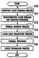
- FIG. 1 shows a flow of a method of manufacturing a nitride semiconductor device according to a first embodiment of the present invention.
- FIG. 2 shows the method of manufacturing the nitride semiconductor device according to the first embodiment of the present invention.
- FIGS. 3A and 3B show the method of manufacturing the nitride semiconductor device according to the first embodiment of the present invention.
- FIG. 4 shows the method of manufacturing the nitride semiconductor device according to the first embodiment of the present invention.
- FIG. 5 shows the method of manufacturing the nitride semiconductor device according to the first embodiment of the present invention.
- FIG. 6 shows the method of manufacturing the nitride semiconductor device according to the first embodiment of the present invention.
- FIG. 7 shows the method of manufacturing the nitride semiconductor device according to the first embodiment of the present invention.
- FIG. 8 shows a method of manufacturing a nitride semiconductor device according to a second embodiment of the present invention.
- FIGS. 9A and 9B show the method of manufacturing the nitride semiconductor device according to the second embodiment of the present invention.
- FIG. 10 shows the method of manufacturing the nitride semiconductor device according to the second embodiment of the present invention.
- FIG. 11 shows the method of manufacturing the nitride semiconductor device according to the second embodiment of the present invention.
- FIG. 12 shows the method of manufacturing the nitride semiconductor device according to the second embodiment of the present invention.
- FIG. 13 shows the method of manufacturing the nitride semiconductor device according to the second embodiment of the present invention.
- FIG. 14 shows a relationship between a wavelength and an absorption coefficient of laser light irradiated to a stripping layer.
- FIG. 1 is a flowchart of the method of manufacturing a light-emitting diode according to a first embodiment of the present invention.
- FIGS. 2 to 7 are cross-sectional views of the light-emitting diode according to the first embodiment in the course of manufacturing thereof.
- a process of forming a stripping layer is performed in Step S 10 .
- a stripping layer 10 which is formed of a nitride semiconductor containing In, is formed by use of an MOCVD (Metal Organic Chemical Vapor Deposition) method, on a growth substrate 50 formed of a GaN substrate.
- MOCVD Metal Organic Chemical Vapor Deposition
- the stripping layer 10 which has a thickness of about 20 nm, and which is formed of undoped single crystal Ga 0.7 In 0.3 N, is formed on the growth substrate 50 by use of a source gas of NH 3 , TMGa (trimethylgallium) and TMIn (trimethylindium).
- the stripping layer 10 be formed of InGaN containing In with the In composition ratio of not less than 18%. Moreover, it is more preferable that the stripping layer 10 be formed of InGaN containing In with the In composition ratio of not more than 30%.
- Step S 11 a process of forming a nitride semiconductor layer and a decomposition process for causing the decomposition of the stripping layer are performed.
- the nitride semiconductor layer 100 is formed on the stripping layer 10 by use of the MOCVD method. Thereafter, the stripping layer 10 is caused the decomposition.
- the nitride semiconductor layer 100 is formed of an under layer 11 , an n-type contact layer 12 , an n-type cladding layer 13 , an active layer 14 , a p-type cap layer 15 , a p-type cladding layer 16 , and a p-type contact layer 17 , which are formed from the side of the stripping layer 10 in the above order.
- the decomposition process is performed by causing indium nitride (InN), metal In and metal Ga in the stripping layer 10 to be segregated at the time when the under layer 11 is formed on the stripping layer 10 on the growth substrate 50 .
- the decomposition process is performed after the nitride semiconductor layer 100 is formed.
- the under layer 11 which has a thickness of about 1.0 ⁇ m, and which is formed of undoped single crystal GaN, is formed on the stripping layer 10 by use of source gas formed of NH 3 and TMGa in a state where the growth substrate 50 is maintained at a growth temperature between about 1000° C. and about 1200° C. (for example, 1150° C.).
- a decomposition of the stripping layer 10 which is considered as phase separation, is caused and the stripping layer 10 is blackened, when the under layer 11 is formed on the stripping layer 10 on the growth substrate 50 .
- the decomposition of the stripping layer 10 includes concept that the generation of defects (energy level caused by the defects) and segregation of metal Ga, metal In, and InN.
- the decomposition of the stripping layer 10 is considered as a factor of increasing absorption coefficient and lengthening a wavelength of an absorption edge.
- the n-type cladding layer 13 is formed on the n-type contact layer 12 by use of source gas, which is formed of NH 3 , TMGa (trimethylgallium) and TMAl (trimethylaluminum), and dopant gas, which is formed of SiH 4 , in a state where the growth substrate 50 is maintained at a growth temperature between about 1000° C. and about 1200° C. (for example, 1150° C.).
- the n-type cladding layer 13 has a thickness of about 0.15 ⁇ m, and is formed of single crystal Al 0.1 Ga 0.9 N doped with Si.
- well layers and barrier layers are alternately formed on the n-type cladding layer 13 by use of source gas formed of NH 3 , TMG and TMIn.
- Each of the well layers has a thickness of about 5 nm, and is formed of undoped single crystal Ga 0.9 In 0.1 N
- each of the barrier layers has a thickness of about 10 nm, and is formed of undoped single crystal GaN.
- the active layer 14 which has an MQW (Multiple-Quantum Well) structure including three well layers, can be formed.
- the p-type cap layer which has a thickness of about 10 nm, and which is formed of single crystal Al 0.1 Ga 0.9 N doped with Mg, is formed on the active layer 14 by adding source gas, which is formed of NH 3 , TMGa and TMIn, and dopant gas which is formed of CP 2 Mg.
- the p-type cladding layer 16 which has a thickness of about 0.1 ⁇ m, and which is formed of single crystal Al 0.1 Ga 0.9 N doped with Mg, is formed on the p-type cap layer by use of source gas, which is formed of NH 3 , TMGa and TMAl, and dopant gas formed of CP 2 Mg.
- the p-type contact layer 17 which has a thickness of about 5 nm, and which is formed of single crystal Ga 0.95 In 0.05 N doped with Mg, is formed on the p-type cladding layer 16 by use of source gas, which is formed of NH 3 , TMGa and TMIn, and dopant gas formed of CP 2 Mg.
- the p-type cap layer, the p-type cladding layer 16 and the p-type contact layer 17 are respectively made into p-type layers by a thermal treatment or an electron beam treatment given thereto.
- the nitride semiconductor layer 100 is formed of the under layer 11 , the n-type contact layer 12 , the n-type cladding layer 13 , the active layer 14 , the p-type cap layer 15 , the p-type cladding layer 16 , and the p-type contact layer 17 .
- a decomposition of the stripping layer 10 which is considered as phase separation, is caused and the stripping layer 10 is blackened, by maintaining the growth substrate 50 at a high temperature.
- the decomposition of the stripping layer 10 includes concept that the generation of defects (energy level caused by the defects) and segregation of metal Ga, metal In, and InN.
- the decomposition of the stripping layer 10 is considered as a factor of increasing absorption coefficient and lengthening a wavelength of an absorption edge.
- the stripping layer 10 after the decomposition caused it is considered that indium nitride (InN), metal In and metal Ga are segregated.
- the band-gap energy of indium nitride (InN) is about 0.7 eV, and the band-gap energy of metal In and metal Ga are also low.
- the band-gap energy of the stripping layer 10 can be lowered. That is, the band-gap energy of the stripping layer 10 can be lowered without adjusting a composition ratio thereof for In and the like contained in the stripping layer 10 .
- the decomposition process for causing the decomposition of the stripping layer 10 may be performed at any time, as long as the decomposition process is performed after the under layer 11 is formed at least on a surface of the stripping layer 10 when the decomposition process does not influence the formation of the nitride semiconductor layer 100 .
- the stripping layer 10 be caused the decomposition at the time when the under layer 11 is formed on the stripping layer 10 as shown in FIG. 3A .
- a temperature, at which InN in the stripping layer 10 is segregated, can be controlled by changing a content of In, a thickness of the stripping layer 10 , a stack structure and the like in the stripping layer 10 .
- the decomposition process is performed by the segregation of indium nitride (InN), metal In and metal Ga and the generation of the defects in the stripping layer 10 , when the under layer 11 is formed on the stripping layer 10 on the growth substrate 50 .
- the decomposition process for causing the decomposition of the stripping layer 10 may be performed after the nitride semiconductor layer 100 is formed. Otherwise, the decomposition process may be performed on the stripping layer 10 while the nitride semiconductor layer 100 is being formed.
- Step S 12 a thermal bonding process is preformed.
- a p-type electrode 18 is formed on the p-type contact layer 17 .
- a supporting substrate 51 including a bonding layer 52 is thermally bonded.
- the p-type electrode 18 is configured of three layers of Ag, Pt, Au layers which respectively have thicknesses of about 200 nm, about 200 nm, and about 500 nm, and which are formed from the side of the p-type contact layer 17 in the above order.
- the three layers are formed on the p-type contact layer 17 respectively by a vacuum evaporation method.
- a nitride semiconductor device 200 is formed by forming the p-type electrode 18 on the nitride semiconductor layer 100 .
- the supporting substrate 51 is formed of Si, and has a thickness of about 200 ⁇ m.
- the bonding layer 52 formed on the supporting substrate 51 is constituted of three layers of Ti, Pd and Au layers, which respectively have thicknesses of about 10 nm, about 50 and about 500 nm, and which are formed from the side of the supporting substrate 51 in the above order.
- the three layers are formed respectively by the vacuum evaporation method.
- the Au layer of the p-type electrode 18 and that of the bonding layer 52 are thermally bonded to each other by use of solder formed of Au—Sn, Pd—Sn, In—Sn or the like, or by use of conductive paste formed of Ag.
- solder formed of Au—Sn in a case of joining the above Au layers to each other with solder formed of Au—Sn (in a composition ratio of 80% Au to 20% Sn)
- the growth substrate 50 and the supporting substrate 51 are heated to about 300° C., and are maintained under pressure of about 0.3 Pa for several dozens of minutes. Thereby, the two Au layers are thermally bonded to each other.
- Step S 13 a laser irradiating process is performed.
- the stripping layer 10 is decomposed into In, Ga and N 2 to be a separation layer 10 b.
- the stripping layer 10 is first irradiated from the side of the growth substrate 50 with a second harmonic having 2.3 eV of the photon energy.
- a second harmonic includes Nd:YAG (Neodymium:Yttrium-Aluminium-Garnet) laser light and Nd:YVO 4 laser light.
- the irradiation is performed with an energy density of the laser light between about 200 mJ/cm ⁇ 2 and about 1000 mJ/cm ⁇ 2 , and the laser light is absorbed into the stripping layer 10 .
- a part of the under layer 11 and the stripping layer 10 are decomposed into In, Ga and N 2 to be a separation layer 10 b.
- the photon energy of the laser light be lower than the band-gap energy of the nitride semiconductor layer 100 .
- Step S 14 the thermal treatment is performed in Step S 14 .
- the growth substrate 50 is separated from the nitride semiconductor device 200 by heating the nitride semiconductor device 200 .
- the growth substrate 50 is separated from the nitride semiconductor device 200 by heating the nitride semiconductor device 200 to about 200° C., and thereby causing In and Ga of the separating layer 10 b to be in a molten state.
- the separation layer 10 b and the under layer 11 are removed for the n-type contact layer 12 to be exposed.
- Step S 15 a process of splitting the device is performed.
- an n-type electrode 19 is formed on the n-type contact layer 12 of the nitride semiconductor layer 100 .
- the nitride semiconductor device 200 is split.
- the translucent n-type electrode 19 is formed on the n-type contact layer 12 by use of the vacuum evaporation method.
- the n-type electrode 19 is formed of a Ti layer having a thickness of about 1 nm and an Al layer having a thickness of about 5 nm.
- device separation is performed by dividing the nitride semiconductor device 200 by dicing with laser scribing, or with selective etching, on the supporting substrate 51 along separation lines 53 perpendicular to a plane of the supporting substrate 51 on which the nitride semiconductor layer 100 is grown.
- the light-emitting diode of the first embodiment according to the present invention can be obtained.
- the stripping layer 10 is formed on the growth substrate 50 , and the temperature thereof is increased. Thereby, the band-gap energy of the stripping layer 10 can be lowered without adjusting a composition ratio of the stripping layer 10 .
- the photon energy of the laser light can be made sufficiently lower than the band-gap energy of the growth substrate 50 even when the photon energy of the laser light is made larger than the band-gap energy of the stripping layer 10 .
- influence exerted upon the growth substrate 50 by the photon energy of the laser light is smaller, and the nitride semiconductor layer 100 can be separated easily from the growth substrate 50 while reducing decomposition and cracking of the growth substrate 50 and degradation in characteristics of the nitride semiconductor devices 200 , which stem from a defect, an impurity or the like in the growth substrate 50 .
- the laser light permeates the stripping layer 10 to reach the nitride semiconductor layer 100 , degradation in characteristics of the nitride semiconductor devices 200 can be reduced due to the low photon energy of the laser light.
- the stripping layer 10 of InGaN containing In with the In composition ratio of not less than 18%, the stripping layer 10 can be caused the decomposition easily. Thereby, the laser light is more likely to be absorbed into the stripping layer 10 after the decomposition caused. Hence, the band-gap energy of the stripping layer can be lowered.
- the stripping layer 10 of InGaN containing In with the In composition ratio of not more than 30%, the nitride semiconductor layer 100 can be formed easily on the stripping layer 10 .
- the photon energy of the laser light is lower than the band-gap energy of each of layers forming the nitride semiconductor layer 100 . Thereby, it is more difficult for the laser light to be absorbed into the respective layers forming the nitride semiconductor layer 100 . Thus, it is made possible to reduce damage, which the laser light exerts on the nitride semiconductor layer 100 .
- the photon energy of the laser light is not less than 0.8 eV.
- the photon energy of the laser light is even higher than the band-gap energy of the stripping layer 10 after the decomposition caused formed of the nitride semiconductor containing In.
- the laser light is sufficiently absorbed into the stripping layer 10 after the decomposition caused, and decomposes the stripping layer 10 more. It is therefore easier to separate the growth substrate 50 and the nitride semiconductor layer 100 from each other.
- the photon energy of the laser light is not less than 2.7 eV, damage to the growth substrate 50 can be reduced. Thereby, it is made possible to reuse the growth substrate 50 .
- steps of a method of manufacturing a nitride semiconductor laser according to a second embodiment of the present invention will be further described respectively with reference to FIG. 1 , and FIGS. 8 to 13 .
- the nitride semiconductor layer 100 is configured of the under layer 11 , the n-type contact layer 12 , the n-type cladding layer 13 , the active layer 14 , the p-type cap layer 15 , the p-type cladding layer 16 , and the p-type contact layer 17 .
- a nitride semiconductor layer 101 is configured of an under layer 21 , an n-type contact layer 22 , an n-type cladding layer 23 , an n-type optical guiding layer 30 , an active layer 24 , a p-type cap layer 25 , a p-type optical guiding layer 31 , a p-type cladding layer 26 , and a p-type contact layer 27 .
- ridge portions 64 , a current blocking layer 32 , a p-side ohmic electrode 33 and a p-side pad electrode 34 are additionally formed thereon.
- the second embodiment is different in that layers constituting the nitride semiconductor layer 101 include the n-type optical guiding layer 30 and the p-type optical guiding layer 31 , and in that the ridge portions 64 , the current blocking layer 32 , the p-side ohmic electrode 33 and the p-side pad electrode 34 are formed thereon.
- FIGS. 8 to 13 are cross-sectional views of the nitride semiconductor laser according to the second embodiment in the course of manufacturing thereof.
- Step S 10 a process of forming a stripping layer is performed.
- a stripping layer 20 which is formed of a nitride semiconductor containing In, is formed on a growth substrate 60 formed of a GaN substrate as in the case with the first embodiment.
- Step S 11 as in the case with the first embodiment, a process of forming a semiconductor layer and a decomposition process for causing the decomposition of the stripping layer are performed.
- the nitride semiconductor layer 101 is formed on the stripping layer 20 by use of the MOCVD method as in the case with the first embodiment.
- the decomposition process for causing the decomposition of the stripping layer 20 is performed.
- the nitride semiconductor layer 101 is formed of the under layer 21 , the n-type contact layer 22 , the n-type cladding layer 23 , the n-type optical guiding layer 30 , the active layer 24 , the p-type cap layer 25 , the p-type optical guiding layer 31 , the p-type cladding layer 26 , and the p-type contact layer 27 which are formed from the side of the stripping layer 20 in the above order.
- the decomposition process is performed, as shown in FIG. 9A , after the under layer 21 is formed on the stripping layer 20 as in the case with the first embodiment.
- the decomposition process may be performed after, or during, the formation of the nitride semiconductor layer 101 , as shown in FIG. 9B .
- the n-type cladding layer 23 is formed on the n-type contact layer 22 by use of source gas, which is formed of NH 3 , TMGa and TMAl, and dopant gas, which is formed of SiH 4 , in a state where the growth substrate 60 is maintained at a growth temperature between about 1000° C. and about 1200° C. (for example, 1150° C.).
- the n-type cladding layer 23 has a thickness of about 1 ⁇ m, and is formed of single crystal Al 0.07 Ga 0.93 N doped with Si.
- the n-type optical guiding layer 30 is grown on the n-type cladding layer 23 by use of source gas, which is formed of NH 3 and TMG, and dopant gas formed of SiH 4 .
- the n-type optical guiding layer 30 has a thickness of about 0.1 ⁇ m, and is formed of single crystal GaN doped with Si.
- well layers and barrier layers are alternately formed on the n-type optical guiding layer 30 by use of source gas formed of NH 3 , TMG and TMIn.
- Each of the well layers has a thickness of about 3.5 nm, and is formed of undoped single crystal Ga 0.85 In 0.15 N.
- Each of the barrier layers has a thickness of about 20 nm, and is formed of undoped single crystal Ga 0.95 In 0.05 N.
- the p-type cap layer 24 which has a thickness of about 20 nm, and which is formed of single crystal Al 0.25 Ga 0.75 N doped with Mg, is formed on the active layer 24 by use of source gas formed of NH 3 , TMGa and TMIn.
- the p-type optical guiding layer 31 is formed on the p-type cap layer 25 by use of source gas, which is formed of NH 3 and TMGa, and dopant gas formed of CP 2 Mg.
- the p-type optical guiding layer 31 has a thickness of about 0.1 ⁇ m, and is formed of single crystal GaN doped with Si.
- the p-type cladding layer 26 is formed on the p-type cap layer 25 by use of source gas, which is formed of NH 3 , TMGa and TMAl, and dopant gas formed of CP 2 Mg.
- source gas which is formed of NH 3 , TMGa and TMAl
- dopant gas formed of CP 2 Mg dopant gas formed of CP 2 Mg.
- the p-type cladding layer 26 has a thickness of about 0.5 ⁇ m, and is formed of single crystal Al 0.07 Ga 0.93 N doped with Mg.
- the p-type contact layer 27 is formed on the p-type cladding layer 26 by use of source gas, which is formed of NH 3 , TMGa and TMIn, and dopant gas which is formed of CP 2 Mg.
- source gas which is formed of NH 3 , TMGa and TMIn
- dopant gas which is formed of CP 2 Mg.
- the p-type contact layer 27 has a thickness of about 3 nm, and is formed of single crystal Ga 0.99 In 0.01 N doped with Mg.
- the p-type cap layer 25 , the p-type optical guiding layer 31 , the p-type clad later 26 , and the p-type contact layer 27 are respectively made into p-type layers by a thermal treatment or an electron beam treatment given thereto as in the case with the first embodiment.
- the nitride semiconductor layer 101 is formed of the under layer 21 , the n-type contact layer 22 , the n-type cladding layer 33 , the n-type optical guiding layer 30 , the active layer 24 , the p-type cap layer 25 , the p-type optical guiding layer 31 , the p-type cladding layer 26 , and the p-type contact layer 27 .
- the ridge portions 64 are formed by respectively removing predetermined regions of the p-type cladding layer 26 and of the p-type contact layer 27 . Specifically, a fine pattern of stripes, each of which has a width of about 1.5 ⁇ m, and each of which extends in a [1-100] direction, is formed by use of a photolithography technique. Thereafter, the predetermined regions of the p-type cladding layer 26 and of the p-type contact layer 27 are removed by reactive ion etching with a chlorine-based gas. Thereby, the ridge portions 64 each having a width of about 1.5 ⁇ m are formed. On this occasion, a depth of the reactive ion etching is controlled in order that a thickness of a plane portion of the p-type cladding layer 26 excluding the ridge portions 64 thereof is about 0.05 ⁇ m.
- the current blocking layer 32 is formed on the p-type cladding layer 26 .
- a SiO 2 film is formed so as to cover a plane exposing the p-type cladding layer 26 and p-type contact layer 27 .
- the SiO 2 film is provided with the ridge portions 64 of the nitride semiconductor layer 100 , and has a thickness of about 0.2 ⁇ m.
- the current blocking layer 32 is formed by removing the SiO 2 film above an upper plane of the p-type contact layer 27 in convex portions of the ridge portions 64 by a photolithography technique, and by reactive ion etching with a CF 4 gas.
- the p-side ohmic electrode 33 is formed on the current blocking layer 32 and on the p-type contact layer 27 .
- the p-side ohmic electrode 33 which is formed of a Pt layer, a Pd layer, an Au layer and a Ni layer, is formed in stripes by the vacuum evaporation method.
- the Pt layer has a thickness of about 1 nm on the p-type contact layer 27 from an upper side of the p-type contact layer 27
- the Pd layer has a thickness of about 100 nm
- the Au layer has a thickness of about 240 nm
- the Ni layer has a thickness of about 240 nm.
- the p-side pad electrode 34 is formed so as to cover a portion above the current blocking layer 32 as well as the p-side ohmic electrode 33 .
- the p-side pad electrode 34 which is formed of a Ti layer, a Pt layer, an Au layer, is formed.
- the above layers of Ti, Pt, and Au respectively have the thicknesses of about 100 nm, about 150 nm and about 3 ⁇ m, and are formed from the side of the current blocking layer 32 in the above order.
- Step S 12 a thermal bonding process is preformed.
- a supporting substrate 61 including a bonding layer 62 is thermally bonded onto the nitride semiconductor devices 201 as in the case with the first embodiment.
- Step S 13 a laser irradiating process is performed.
- the stripping layer 20 is decomposed into In, Ga and N 2 to be a separation layer 20 b.
- Step S 14 A thermal treatment is performed in Step S 14 .
- the growth substrate 60 is separated from the nitride semiconductor device 201 by heating the nitride semiconductor devices 201 as in the case with the first embodiment.
- the separation layer 20 b and the under layer 21 are removed for the n-type contact layer 22 to be exposed.
- Step S 15 a process of splitting the device is performed.
- an n-side ohmic electrode 35 is formed on predetermined regions on the n-type contact layer 22 of the nitride semiconductor layer 101 .
- the n-side ohmic electrode 35 which is formed of an Al layer, a Ni layer and an Au layer, is formed on the n-type contact layer 22 by use of the vacuum evaporation method.
- the above layers of Al, Ni and Au respectively have the thicknesses of about 6 nm, about 10 and about 700 nm.
- an n-side pad electrode 36 which is formed of a Ni layer and an Au layer, is formed on the n-side ohmic electrode 35 .
- the above layers of Ni and Au respectively have the thicknesses of about 10 and about 100 nm.
- scribing is performed along separation lines perpendicular to the stripes of the ridge portions 64 , and along separation lines 63 parallel to the stripes of the ridge portions 64 .
- device separation is performed while forming laser resonance planes, which are orthogonal to the respective stripes of the ridge portions 64 , and which are each formed of a [1-1001] plane and a [-1100] plane.
- the nitride semiconductor laser of the second embodiment according to the present invention can be obtained.
- FIG. 14 shows the relationship between the wavelength and the absorption ratio of the stripping layer before and after the decomposition caused. Note that, horizontal axis shows the wavelength of the light and vertical axis shows absorption ratio of the light, in the FIG. 14 .
- the wavelength band where the stripping layer absorbs the laser light sufficiently is short wavelength side only.
- the stripping layer before the decomposition caused only the laser light of 400 nm or shorter can be used, to obtain the absorption ratio of 0.4 or more.
- the wavelength band where the stripping layer absorbs the laser light sufficiently is expanded to the long wavelength side compared to the stripping layer before the decomposition caused.
- the absorption ratio of 0.4 or more can be obtained in the wavelength of 1100 nm or lower.
- the methods of manufacturing a light-emitting diode and a semiconductor laser, each of which utilizes light emitted from an active layer of a nitride semiconductor layer have been exemplified in the first and second embodiments.
- the present invention is not limited to the above.
- the present invention can also be employed for a method of manufacturing light-emitting devices with which a fluorescent substance using light emitted from each of these light-emitting devices as excitation light are combined.
- the present invention is also applicable in: an electronic device such as an HEMT (High Electron Mobility Transistor) including a nitride semiconductor layer; a SAW (Surface Acoustic Wave) device; and a light receiving element.
- HEMT High Electron Mobility Transistor
- SAW Surface Acoustic Wave
- the present invention is applicable to a multi-wavelength semiconductor laser by applying thereto a technique of replacing a growth substrate according to the present invention. Accordingly, it is made possible to increase a yield in intervals between light-emitting points within a plane of a wafer in the multi-wavelength semiconductor laser.
- the descriptions are provided for the case where the nitride semiconductor layer is grown by use of the MOCVD method.
- the nitride semiconductor layer may be grown by use of an HVPE method, a gas-source MBE method, or the like.
- a crystalline structure of each of the nitride semiconductor layers may be a wurtzite structure or a zinc-blende structure.
- a plane orientation of growth for each of the layers is not limited to [0001], and may be [11-20] or [1-100].
- a GaN substrate is used as the growth substrate for the nitride semiconductor layer.
- a substrate, on which the nitride semiconductor layer can be grown such as a SiC, ZnO, LAO, spinel, sapphire, or Al X Ga 1-X N (0 ⁇ X ⁇ 1) substrate, is usable.
- a layer formed of InGaN is exemplified as the stripping layer in each of the first and second embodiments.
- the present invention is not limited to the above.
- InAlN or InGaAlN is also usable. With any one of these mixed crystals containing Al, not only causing the decomposition of the stripping layer is easier, but also lattice constant differences of the stripping layer with the growth substrate and the nitride semiconductor layer can be eased by appropriately setting a composition ratio of the stripping layer.
- the stripping layer may have a multilayered structure.
- a superlattice structure may be formed therein by superposing a layer in a composition ratio relatively rich in In, and a layer which contains no In, or which is in a composition ratio relatively low in In.
- a superlattice structure formed of, for example, AlGaN and GaN is still more effective in reducing distortion of the nitride semiconductor layer.
- a method, which uses thermal decomposition by heating in a growing phase of the nitride semiconductor layer is exemplified as a method of the decomposition.
- the present invention is not limited to the above.
- a method using heating after growth of the nitride semiconductor layer, a method using light irradiation, or a method using electron beam irradiation can be employed. This is because a temperature of the nitride semiconductor layers can be increased also by the laser light or by the electron beam.
- the second harmonic of Nd:YAG (or, Nd:YVO 4 or the like) laser light is exemplified as the laser light used for separation of the substrate.
- the present invention is not limited to the above.
- a fundamental harmonic of the laser light is also usable, and it is possible to reduce degradation of the nitride semiconductor layer by using femto second pulse laser light which is a ultra-short pulse light using a Ti sapphire laser, the degradation resulting from distortion thereof associated with heat generation at the time of laser light irradiation.
- ruby laser and a CO/CO 2 laser may be used as a laser irradiating the laser light to the stripping layer.
- the supporting substrate is not limited to that of Si, it is preferable that the supporting substrate be electrically conductive.
- a conductive semiconductor Si, SiC, GaAs, ZnO, or the like
- a metal or a composite metal Al, Fe—Ni, Cu—W, Cu—Mo, or the like
- a composite material containing a metal and a metallic oxide Cu—CuO
- a metal-based material is excellent in mechanical characteristics, is less breakable, and is therefore more suitable as the supporting substrate, as compared to a semiconductor material.
Abstract
Description
Claims (18)
Applications Claiming Priority (6)
| Application Number | Priority Date | Filing Date | Title |
|---|---|---|---|
| JPJP2005-276854 | 2005-09-22 | ||
| JP2005276854 | 2005-09-22 | ||
| JP2005-276854 | 2005-09-22 | ||
| JPJP2006-249883 | 2006-09-14 | ||
| JP2006249883A JP2007116110A (en) | 2005-09-22 | 2006-09-14 | Method for manufacturing nitride semiconductor device |
| JP2006-249883 | 2006-09-14 |
Publications (2)
| Publication Number | Publication Date |
|---|---|
| US20070066037A1 US20070066037A1 (en) | 2007-03-22 |
| US7759219B2 true US7759219B2 (en) | 2010-07-20 |
Family
ID=37429254
Family Applications (1)
| Application Number | Title | Priority Date | Filing Date |
|---|---|---|---|
| US11/524,258 Expired - Fee Related US7759219B2 (en) | 2005-09-22 | 2006-09-21 | Method of manufacturing nitride semiconductor device |
Country Status (5)
| Country | Link |
|---|---|
| US (1) | US7759219B2 (en) |
| EP (1) | EP1768194B1 (en) |
| JP (1) | JP2007116110A (en) |
| CN (1) | CN1937271B (en) |
| AT (1) | ATE518256T1 (en) |
Families Citing this family (10)
| Publication number | Priority date | Publication date | Assignee | Title |
|---|---|---|---|---|
| US20080303033A1 (en) * | 2007-06-05 | 2008-12-11 | Cree, Inc. | Formation of nitride-based optoelectronic and electronic device structures on lattice-matched substrates |
| JP4937025B2 (en) * | 2007-07-20 | 2012-05-23 | 三洋電機株式会社 | Semiconductor laser device and manufacturing method thereof |
| US7915643B2 (en) * | 2007-09-17 | 2011-03-29 | Transphorm Inc. | Enhancement mode gallium nitride power devices |
| JP2010177390A (en) * | 2009-01-29 | 2010-08-12 | Sony Corp | Method of transferring device and method of manufacturing display apparatus |
| JP5771968B2 (en) * | 2010-04-09 | 2015-09-02 | 住友電気工業株式会社 | Manufacturing method of semiconductor device, laminated support substrate for epitaxial growth, and laminated support substrate for device |
| CN102699537B (en) * | 2012-05-18 | 2015-11-04 | 杭州士兰明芯科技有限公司 | The system and method for laser lift-off LED substrate |
| JP2013128150A (en) * | 2013-03-26 | 2013-06-27 | Toyoda Gosei Co Ltd | Method of manufacturing group-iii nitride semiconductor light-emitting element |
| FR3009644B1 (en) * | 2013-08-08 | 2016-12-23 | Soitec Silicon On Insulator | METHOD, STACK AND ASSEMBLY FOR SEPARATING A STRUCTURE OF A SUBSTRATE BY ELECTROMAGNETIC IRRADIATION |
| CN106887505B (en) * | 2017-04-24 | 2019-07-16 | 芜湖聚飞光电科技有限公司 | A kind of production method of single side luminescence chip grade LED |
| DE102018202707A1 (en) | 2018-02-22 | 2019-08-22 | Fraunhofer-Gesellschaft zur Förderung der angewandten Forschung e.V. | Generation of panoramic pictures |
Citations (8)
| Publication number | Priority date | Publication date | Assignee | Title |
|---|---|---|---|---|
| US5851905A (en) * | 1996-07-11 | 1998-12-22 | North Carolina State University | Methods of forming indium gallium nitride or aluminum indium gallium nitride using controlled hydrogen gas flows |
| JP2000101139A (en) | 1998-09-25 | 2000-04-07 | Toshiba Corp | Semiconductor light-emitting element, manufacture thereof and device using the same |
| US6071795A (en) | 1998-01-23 | 2000-06-06 | The Regents Of The University Of California | Separation of thin films from transparent substrates by selective optical processing |
| JP2002338398A (en) | 2001-05-18 | 2002-11-27 | Matsushita Electric Ind Co Ltd | Method for producing nitride semiconductor substrate and method for producing nitride semiconductor device |
| JP2004072052A (en) | 2002-08-09 | 2004-03-04 | Matsushita Electric Ind Co Ltd | Semiconductor device and manufacturing method thereof |
| EP1505661A2 (en) | 2003-08-08 | 2005-02-09 | Sumitomo Electric Industries, Ltd. | GaN-based LED and its manufacturing method |
| US20050059178A1 (en) | 2003-09-17 | 2005-03-17 | Erchak Alexei A. | Light emitting device processes |
| CN1666319A (en) | 2002-07-02 | 2005-09-07 | 日本电气株式会社 | Group III nitride semiconductor substrate and its manufacturing method |
Family Cites Families (4)
| Publication number | Priority date | Publication date | Assignee | Title |
|---|---|---|---|---|
| JP2001119104A (en) * | 1999-10-21 | 2001-04-27 | Matsushita Electric Ind Co Ltd | Method for manufacturing semiconductor |
| JP2002319702A (en) * | 2001-04-19 | 2002-10-31 | Sony Corp | Method of manufacturing nitride semiconductor element and nitride semiconductor element |
| US6455340B1 (en) * | 2001-12-21 | 2002-09-24 | Xerox Corporation | Method of fabricating GaN semiconductor structures using laser-assisted epitaxial liftoff |
| US7056810B2 (en) * | 2002-12-18 | 2006-06-06 | Semiconductor Energy Laboratory Co., Ltd. | Method for manufacturing semiconductor apparatus, and semiconductor apparatus and electric appliance |
-
2006
- 2006-09-14 JP JP2006249883A patent/JP2007116110A/en active Pending
- 2006-09-21 US US11/524,258 patent/US7759219B2/en not_active Expired - Fee Related
- 2006-09-22 CN CN2006101543636A patent/CN1937271B/en not_active Expired - Fee Related
- 2006-09-22 AT AT06254913T patent/ATE518256T1/en not_active IP Right Cessation
- 2006-09-22 EP EP06254913A patent/EP1768194B1/en not_active Not-in-force
Patent Citations (13)
| Publication number | Priority date | Publication date | Assignee | Title |
|---|---|---|---|---|
| US5851905A (en) * | 1996-07-11 | 1998-12-22 | North Carolina State University | Methods of forming indium gallium nitride or aluminum indium gallium nitride using controlled hydrogen gas flows |
| US6071795A (en) | 1998-01-23 | 2000-06-06 | The Regents Of The University Of California | Separation of thin films from transparent substrates by selective optical processing |
| JP2000101139A (en) | 1998-09-25 | 2000-04-07 | Toshiba Corp | Semiconductor light-emitting element, manufacture thereof and device using the same |
| US6303405B1 (en) | 1998-09-25 | 2001-10-16 | Kabushiki Kaisha Toshiba | Semiconductor light emitting element, and its manufacturing method |
| JP2002338398A (en) | 2001-05-18 | 2002-11-27 | Matsushita Electric Ind Co Ltd | Method for producing nitride semiconductor substrate and method for producing nitride semiconductor device |
| CN1666319A (en) | 2002-07-02 | 2005-09-07 | 日本电气株式会社 | Group III nitride semiconductor substrate and its manufacturing method |
| US7189588B2 (en) | 2002-07-02 | 2007-03-13 | Nec Corporation | Group III nitride semiconductor substrate and its manufacturing method |
| JP2004072052A (en) | 2002-08-09 | 2004-03-04 | Matsushita Electric Ind Co Ltd | Semiconductor device and manufacturing method thereof |
| EP1505661A2 (en) | 2003-08-08 | 2005-02-09 | Sumitomo Electric Industries, Ltd. | GaN-based LED and its manufacturing method |
| JP2005093988A (en) | 2003-08-08 | 2005-04-07 | Sumitomo Electric Ind Ltd | Semiconductor light-emitting device and method of manufacturing the same |
| US20050040425A1 (en) | 2003-08-08 | 2005-02-24 | Katsushi Akita | Light generating semiconductor device and method of making the same |
| CN1581525A (en) | 2003-08-08 | 2005-02-16 | 住友电气工业株式会社 | Light-emitting semiconductor device and its manufacturing method |
| US20050059178A1 (en) | 2003-09-17 | 2005-03-17 | Erchak Alexei A. | Light emitting device processes |
Non-Patent Citations (4)
| Title |
|---|
| Applied Physics Letter vol. 85, No. 11 1961-1963; Compositional dependence of phase separation in InGaN Layers; M. Rao, et al. |
| Chinese Search Report and Office Action for corresponding application, dated Sep. 4, 2009, English Translations included. |
| European Search Report from corresponding European case, dated Nov. 5, 2009. |
| Journal of Crystal Growth 289 (2006) 107-112; Improvement of green LED by growing p-GaN on in 0.25GaN MQWs at low temperature; Min-Suk Oh, et al. |
Also Published As
| Publication number | Publication date |
|---|---|
| EP1768194A2 (en) | 2007-03-28 |
| EP1768194A3 (en) | 2009-12-09 |
| CN1937271B (en) | 2011-03-09 |
| EP1768194B1 (en) | 2011-07-27 |
| CN1937271A (en) | 2007-03-28 |
| JP2007116110A (en) | 2007-05-10 |
| US20070066037A1 (en) | 2007-03-22 |
| ATE518256T1 (en) | 2011-08-15 |
Similar Documents
| Publication | Publication Date | Title |
|---|---|---|
| US7759219B2 (en) | Method of manufacturing nitride semiconductor device | |
| US6841410B2 (en) | Method for forming group-III nitride semiconductor layer and group-III nitride semiconductor device | |
| US7435994B2 (en) | Semiconductor device and method for fabricating the same | |
| US8088637B1 (en) | Method of manufacturing a semiconductor device including a superlattice strain relief layer | |
| KR101646064B1 (en) | Method of manufacture for nitride semiconductor light emitting element, wafer, and nitride semiconductor light emitting element | |
| US8698168B2 (en) | Semiconductor device having aluminum nitride layer with void formed therein | |
| EP1990841B1 (en) | Superlattice strain relief layer for semiconductor devices | |
| US20040065889A1 (en) | Semiconductor wafer, semiconductor device, and methods for fabricating the same | |
| KR102108196B1 (en) | Deep ultraviolet light emitting device separated from growth substrate and method for fabricating the same | |
| JP2004072052A (en) | Semiconductor device and manufacturing method thereof | |
| US9873170B2 (en) | Method of manufacturing light emitting element | |
| US20150228848A1 (en) | Nitride semiconductor light-emitting element and method for producing same | |
| US20050042788A1 (en) | Semiconductor device and method for manufacturing the same | |
| US20100051939A1 (en) | Nitride based semiconductor device and method of manufacturing the same | |
| JP2007221051A (en) | Manufacturing method of nitride-based semiconductor element | |
| JP2003046201A (en) | Semiconductor laser element and method of manufacturing the same | |
| JP4631214B2 (en) | Manufacturing method of nitride semiconductor film | |
| US7550757B2 (en) | Semiconductor laser and method for manufacturing semiconductor laser | |
| JPH11274563A (en) | Semiconductor device and semiconductor light emitting device | |
| JP2003264314A (en) | Semiconductor device and its manufacturing method | |
| JP2009238834A (en) | Support substrate having nitride-based semiconductor layer, and method of forming same | |
| JP2000332293A (en) | Iii-v nitride semiconductor light emitting element and its manufacture | |
| JP2003218468A (en) | Semiconductor laser element and manufacturing method therefor | |
| JP4740902B2 (en) | Manufacturing method of semiconductor device | |
| JP2007300146A (en) | Semiconductor device and its manufacturing method |
Legal Events
| Date | Code | Title | Description |
|---|---|---|---|
| AS | Assignment |
Owner name: SANYO ELECTRIC CO., LTD., JAPAN Free format text: ASSIGNMENT OF ASSIGNORS INTEREST;ASSIGNORS:KUNOH, YASUMITSU;TAKEUCHI, KUNIO;REEL/FRAME:018331/0357 Effective date: 20060921 |
|
| STCF | Information on status: patent grant |
Free format text: PATENTED CASE |
|
| FEPP | Fee payment procedure |
Free format text: PAYOR NUMBER ASSIGNED (ORIGINAL EVENT CODE: ASPN); ENTITY STATUS OF PATENT OWNER: LARGE ENTITY |
|
| AS | Assignment |
Owner name: FUTURE LIGHT, LLC, CALIFORNIA Free format text: ASSIGNMENT OF ASSIGNORS INTEREST;ASSIGNOR:SANYO ELECTRIC CO., LTD.;REEL/FRAME:027957/0258 Effective date: 20120308 |
|
| FPAY | Fee payment |
Year of fee payment: 4 |
|
| AS | Assignment |
Owner name: SANYO ELECTRIC CO., LTD., JAPAN Free format text: ASSIGNMENT OF ASSIGNORS INTEREST;ASSIGNOR:FUTURE LIGHT LIMITED LIABILITY COMPANY;REEL/FRAME:040523/0797 Effective date: 20161020 |
|
| AS | Assignment |
Owner name: EPISTAR CORPORATION, TAIWAN Free format text: ASSIGNMENT OF ASSIGNORS INTEREST;ASSIGNOR:SANYO ELECTRIC CO., LTD.;REEL/FRAME:041652/0122 Effective date: 20170131 |
|
| MAFP | Maintenance fee payment |
Free format text: PAYMENT OF MAINTENANCE FEE, 8TH YEAR, LARGE ENTITY (ORIGINAL EVENT CODE: M1552) Year of fee payment: 8 |
|
| FEPP | Fee payment procedure |
Free format text: MAINTENANCE FEE REMINDER MAILED (ORIGINAL EVENT CODE: REM.); ENTITY STATUS OF PATENT OWNER: LARGE ENTITY |
|
| LAPS | Lapse for failure to pay maintenance fees |
Free format text: PATENT EXPIRED FOR FAILURE TO PAY MAINTENANCE FEES (ORIGINAL EVENT CODE: EXP.); ENTITY STATUS OF PATENT OWNER: LARGE ENTITY |
|
| STCH | Information on status: patent discontinuation |
Free format text: PATENT EXPIRED DUE TO NONPAYMENT OF MAINTENANCE FEES UNDER 37 CFR 1.362 |
|
| FP | Lapsed due to failure to pay maintenance fee |
Effective date: 20220720 |