US7755615B2 - Optical shuttered touchscreen and method therefor - Google Patents
Optical shuttered touchscreen and method therefor Download PDFInfo
- Publication number
- US7755615B2 US7755615B2 US11/611,970 US61197006A US7755615B2 US 7755615 B2 US7755615 B2 US 7755615B2 US 61197006 A US61197006 A US 61197006A US 7755615 B2 US7755615 B2 US 7755615B2
- Authority
- US
- United States
- Prior art keywords
- time interval
- optical shutter
- touchscreen
- during
- sensing
- Prior art date
- Legal status (The legal status is an assumption and is not a legal conclusion. Google has not performed a legal analysis and makes no representation as to the accuracy of the status listed.)
- Active, expires
Links
Images


Classifications
-
- G—PHYSICS
- G06—COMPUTING; CALCULATING OR COUNTING
- G06F—ELECTRIC DIGITAL DATA PROCESSING
- G06F3/00—Input arrangements for transferring data to be processed into a form capable of being handled by the computer; Output arrangements for transferring data from processing unit to output unit, e.g. interface arrangements
- G06F3/01—Input arrangements or combined input and output arrangements for interaction between user and computer
- G06F3/03—Arrangements for converting the position or the displacement of a member into a coded form
- G06F3/041—Digitisers, e.g. for touch screens or touch pads, characterised by the transducing means
- G06F3/0412—Digitisers structurally integrated in a display
-
- G—PHYSICS
- G06—COMPUTING; CALCULATING OR COUNTING
- G06F—ELECTRIC DIGITAL DATA PROCESSING
- G06F3/00—Input arrangements for transferring data to be processed into a form capable of being handled by the computer; Output arrangements for transferring data from processing unit to output unit, e.g. interface arrangements
- G06F3/01—Input arrangements or combined input and output arrangements for interaction between user and computer
- G06F3/03—Arrangements for converting the position or the displacement of a member into a coded form
- G06F3/041—Digitisers, e.g. for touch screens or touch pads, characterised by the transducing means
- G06F3/0416—Control or interface arrangements specially adapted for digitisers
- G06F3/04166—Details of scanning methods, e.g. sampling time, grouping of sub areas or time sharing with display driving
-
- G—PHYSICS
- G06—COMPUTING; CALCULATING OR COUNTING
- G06F—ELECTRIC DIGITAL DATA PROCESSING
- G06F3/00—Input arrangements for transferring data to be processed into a form capable of being handled by the computer; Output arrangements for transferring data from processing unit to output unit, e.g. interface arrangements
- G06F3/01—Input arrangements or combined input and output arrangements for interaction between user and computer
- G06F3/03—Arrangements for converting the position or the displacement of a member into a coded form
- G06F3/041—Digitisers, e.g. for touch screens or touch pads, characterised by the transducing means
- G06F3/044—Digitisers, e.g. for touch screens or touch pads, characterised by the transducing means by capacitive means
- G06F3/0443—Digitisers, e.g. for touch screens or touch pads, characterised by the transducing means by capacitive means using a single layer of sensing electrodes
-
- G—PHYSICS
- G09—EDUCATION; CRYPTOGRAPHY; DISPLAY; ADVERTISING; SEALS
- G09G—ARRANGEMENTS OR CIRCUITS FOR CONTROL OF INDICATING DEVICES USING STATIC MEANS TO PRESENT VARIABLE INFORMATION
- G09G3/00—Control arrangements or circuits, of interest only in connection with visual indicators other than cathode-ray tubes
- G09G3/20—Control arrangements or circuits, of interest only in connection with visual indicators other than cathode-ray tubes for presentation of an assembly of a number of characters, e.g. a page, by composing the assembly by combination of individual elements arranged in a matrix no fixed position being assigned to or needed to be assigned to the individual characters or partial characters
- G09G3/34—Control arrangements or circuits, of interest only in connection with visual indicators other than cathode-ray tubes for presentation of an assembly of a number of characters, e.g. a page, by composing the assembly by combination of individual elements arranged in a matrix no fixed position being assigned to or needed to be assigned to the individual characters or partial characters by control of light from an independent source
- G09G3/36—Control arrangements or circuits, of interest only in connection with visual indicators other than cathode-ray tubes for presentation of an assembly of a number of characters, e.g. a page, by composing the assembly by combination of individual elements arranged in a matrix no fixed position being assigned to or needed to be assigned to the individual characters or partial characters by control of light from an independent source using liquid crystals
-
- G—PHYSICS
- G02—OPTICS
- G02F—OPTICAL DEVICES OR ARRANGEMENTS FOR THE CONTROL OF LIGHT BY MODIFICATION OF THE OPTICAL PROPERTIES OF THE MEDIA OF THE ELEMENTS INVOLVED THEREIN; NON-LINEAR OPTICS; FREQUENCY-CHANGING OF LIGHT; OPTICAL LOGIC ELEMENTS; OPTICAL ANALOGUE/DIGITAL CONVERTERS
- G02F1/00—Devices or arrangements for the control of the intensity, colour, phase, polarisation or direction of light arriving from an independent light source, e.g. switching, gating or modulating; Non-linear optics
- G02F1/01—Devices or arrangements for the control of the intensity, colour, phase, polarisation or direction of light arriving from an independent light source, e.g. switching, gating or modulating; Non-linear optics for the control of the intensity, phase, polarisation or colour
- G02F1/13—Devices or arrangements for the control of the intensity, colour, phase, polarisation or direction of light arriving from an independent light source, e.g. switching, gating or modulating; Non-linear optics for the control of the intensity, phase, polarisation or colour based on liquid crystals, e.g. single liquid crystal display cells
- G02F1/133—Constructional arrangements; Operation of liquid crystal cells; Circuit arrangements
- G02F1/1333—Constructional arrangements; Manufacturing methods
- G02F1/13338—Input devices, e.g. touch panels
Definitions
- the present invention generally relates to touchscreens and display drivers, and more particularly relates to optical shuttered touchscreens and their operation.
- PDLC polymer-dispersed liquid crystal
- TN twisted nematic
- Optical shuttering is sometimes used to present information to a user and is particularly adapted to touchscreen operation where the information represents control icons (e.g., forward, reverse, pause, and play control symbols for video operation).
- TN/PDLC displays typically include an electroluminescent (EL) backlight for operation in both high and low ambient light conditions.
- an indium-tin oxide (ITO) ground plane is provided below the TN segment electrodes and above the EL backlight to control the electrical noise and improve the touchscreen operation.
- ITO ground plane increases the thickness of the display and the cost and complexity of the display manufacture.
- the ITO ground plane connection is susceptible to failure, thereby reducing display yield and/or increasing field failure defects.
- the ITO ground plane is not fully transmissive, thereby reducing the brightness and effectiveness of the EL backlight.
- FIG. 1 depicts a mobile communication device having an optically shuttered touchscreen in accordance with an embodiment of the present invention
- FIG. 2 is a cross-sectional diagram of a conventional TN/PDLC touchscreen
- FIG. 3 is a timing diagram for a display driver and a capacitive sensor operating the touchscreen of FIG. 2 in a conventional manner;
- FIG. 4 is a block diagram of an electronic device in accordance with an embodiment of the present invention.
- FIG. 5 is a cross sectional diagram of an optically shuttered touchscreen for use in the electronic device of FIG. 4 in accordance with an embodiment of the present invention.
- FIG. 6 is a timing diagram for the display driver and the capacitive sensor of the electronic device of FIG. 4 in accordance with an embodiment of the present invention.
- a method determines touchscreen inputs in response to sensing tactile inputs on a face of the touchscreen while optically shuttering the touchscreen.
- the method includes the steps of charging a capacitive sensor layer of the touchscreen while providing a drive voltage at a first voltage level to a plurality of optical shutter segments in the display during a first time interval and sensing a charge fluctuation on the capacitive sensor layer while maintaining the drive voltage at substantially zero volts during a second time interval.
- the first and second time intervals combine to form a sensing time interval for sensing touchscreen inputs, and the second time interval is greater than half of the complete sensing time interval.
- a touchscreen system includes a display, a touchscreen input detector, and a display driver.
- the display includes a first layer for sensing tactile inputs on a face of the display and a second layer having a plurality of optical shutter segments.
- the touchscreen input detector is coupled to the first layer of the display and determines a touchscreen input in response to capacitively sensing the tactile inputs for a sensing time interval.
- the display driver is coupled to the second layer of the display and provides a drive voltage at a first voltage level to the plurality of optical shutter segments during a first portion of the sensing time interval and maintains the drive voltage at a second voltage level during a second portion of the sensing time interval.
- the second voltage level is substantially zero volts, and the first portion appended by the second portion is substantially the sensing time interval. In addition, the second portion is greater than half of the sensing time interval.
- FIG. 1 shows a mobile communication device 100 implementing a touchscreen with aligned optical shutter and backlight cells in accordance with an embodiment of the present invention.
- the electronic device shown is a mobile communication device 100 , such as a flip-style cellular telephone
- the touchscreen with aligned optical shutter and backlight cells can also be implemented in cellular telephones with other housing styles, personal digital assistants, television remote controls, video cassette players, household appliances, automobile dashboards, billboards, point-of-sale displays, landline telephones, and other electronic devices.
- the mobile communication device 100 has a first housing 102 and a second housing 104 movably connected by a hinge 106 .
- the first housing 102 and the second housing 104 pivot between an open position and a closed position.
- An antenna 108 transmits and receives radio frequency (RF) signals for communicating with a complementary communication device such as a cellular base station.
- a display 110 positioned on the first housing 102 can be used for functions such as displaying names, telephone numbers, transmitted and received information, user interface commands, scrolled menus, and other information.
- a microphone 112 receives sound for transmission, and an audio speaker 114 transmits audio signals to a user.
- a keyless input device 150 is carried by the second housing 104 .
- the keyless input device 150 is implemented as a touchscreen with a display.
- a main image 151 represents a standard, twelve-key telephone keypad.
- images 152 , 153 , 154 , 156 represent an on/off button, a function button, a handwriting recognition mode button, and a telephone mode button.
- images 157 , 158 , 159 represent a “clear” button, a phonebook mode button, and an “OK” button. Additional or different images, buttons or icons representing modes, and command buttons can be implemented using the keyless input device.
- Each image 151 , 152 , 153 , 154 , 156 , 157 , 158 , 159 is a direct driven pixel, and this keyless input device uses a display with aligned optical shutter and backlight cells to selectively reveal one or more images and provide contrast for the revealed images in both low-light and bright-light conditions.
- a cross section of a conventional touchscreen 200 is depicted with aligned optical shutter and backlight cells and is usable for the keyless input device 150 with the cross-section being a portion of a view taken along line 2 - 2 of FIG. 1 .
- the conventional display 200 is a stack with a user-viewable and user-accessible face 201 and multiple layers below the face 201 , including a graphic coverlay layer 202 and a capacitive sensor layer 204 with an indium-tin oxide (ITO) electrode 205 .
- the graphic coverlay 202 provides an upper layer viewable to and touchable by a user and may provide some glare reduction.
- the capacitive sensor layer 204 senses touchscreen inputs on the graphic coverlay layer 202 of the display 200 .
- Beneath the capacitive sensor layer 204 is a twisted nematic (TN) stack layer 206 including a TN backplane electrode 210 and TN segment electrodes 208 between two substrates 212 , 214 for providing the optical shutter operation of the display 200 .
- the TN backplane electrode 210 and TN segment electrodes 208 are formed of indium-tin oxide (ITO) material to provide both transparency and electrical conductivity for operation of the TN stack.
- ITO indium-tin oxide
- the TN backplane electrode 210 is depicted above the TN segment electrodes 208 , a TN stack layer 206 having the TN backplane electrode 210 below the TN segment electrodes 208 would function similarly.
- the TN stack layer 206 utilizes, for example, twisted nematic (TN) liquid crystal (TNLC) display technology employing TN optical shutter material in an optical shutter layer 213 and the TN segment electrodes 208 to provide optical shutter operation. While TNLC technology is described herein for the optical shuttering operation, the optical shutter layer 213 , sandwiched between the TN backplane electrodes 210 and the TN polymer segment electrodes 208 , can alternatively be made using nematic liquid crystal technology (such as twisted nematic or super twisted nematic liquid crystals), polymer-dispersed liquid crystal technology (PDLC), ferro-electric liquid crystal technology, electrically-controlled birefringent technology, optically-compensated bend mode technology, guest-host technology, and other types of light modulating techniques which use optical shutter material 213 such as TN polymer material, PDLC material, cholesteric material, or electro-optical material.
- nematic liquid crystal technology such as twisted nematic or super twisted
- the electric field created by the electrodes 208 , 210 alter the light transmission properties of the TNLC optical shutter material 213 , and the pattern of the TN segment electrode layer 208 defines pixels of the display. These pixels lay over the images 151 , 152 , 153 , 154 , 156 , 157 , 158 , 159 shown in FIG. 1 .
- the liquid crystal material and dichroic dye in the TNLC material 213 are randomly aligned and absorb most incident light.
- the liquid crystal material and dichroic dye align in the direction of the applied field and transmit substantial amounts of incident light.
- a pixel of the TNLC cell can be switched from a relatively non-transparent state to a relatively transparent state.
- Each pixel can be independently controlled to be closed-shuttered or open-shuttered, depending on the application of an electric field, and the pixels act as “windows” with optical shutters that can be opened or closed, to reveal images underneath (e.g. images 151 , 152 , 153 , 154 , 156 , 157 , 158 , 159 ).
- Beneath the TN stack layer 206 is an electroluminescent (EL) stack layer 216 separated from the TN stack layer 206 by an ITO ground layer 218 .
- the EL stack layer 216 includes a backplane and electrodes which provide backlight for operation of the display 200 in both ambient light and low light conditions by alternately applying a high voltage level, such as one hundred volts, to the backplane and electrode.
- the ITO ground layer 218 is coupled to ground and provides an ITO ground plane 218 for reducing the effect on the capacitive sensor layer 204 of any electrical noise generated by the operation of the EL stack layer 216 or other lower layers within the display 200 .
- Beneath the EL stack layer 216 is a base layer 220 which may include one or more layers such as a force sensing switch layer and/or a flex base layer.
- the various layers 202 , 204 , 206 , 218 , 216 and 220 are adhered together by adhesive layers applied therebetween.
- FIG. 3 Conventional operation of the display 200 is illustrated in FIG. 3 , wherein the charge 302 from the capacitive sensor layer 204 , the voltage 304 of the TN backplane 210 and the voltages 306 , 308 of first and second portions of the TN segment electrodes 208 are depicted.
- a charging voltage is provided to the ITO electrode 205 of the capacitive sensor layer 204 for a first portion 322 of the period 3 10 .
- the charge 302 has two different decay profiles 312 , 314 depending on whether a user's touch is detected on the display 200 .
- the signal-to-noise ratio (SNR) of the capacitive sensing i.e., of the voltage of the detectable charge
- the charge is the multiple of the capacitance (determined from a distance of user's finger from the face 201 ) times the voltage thereof
- the ITO ground plane layer 218 provides some isolation between the high voltage EL backlight layer 216 and the low voltage TN stack layer 206 , thereby increasing the SNR of the capacitive sensing.
- the voltages 304 , 306 , 308 supplied to the TN backplane 210 and the TN segment electrodes 208 are switched between a positive voltage, typically about five volts, and zero volts.
- the voltage 306 of the portion of the TN segment electrodes 208 that are turned “on” to render corresponding portions of the display 200 over such portion of the TN segment electrodes 208 relatively transparent are switched opposite to the voltage 304 of the TN backplane 210 (i.e., when the voltage 304 of the TN backplane is high, the voltage 306 of the “on” portion of the TN segment electrodes 208 is low).
- the voltage 308 of the portion of the TN segment electrodes 208 that are turned “off” optically shutter corresponding portions of the display 200 over such portion of the TN segment electrodes 208 because their voltage is switched in the same manner as the voltage 304 of the TN backplane 210 . It can be seen from FIG. 3 that during period 310 , the voltages 306 , 308 supplied to the TN segment electrodes 208 and the TN backplane 210 are high approximately fifty per cent of the time period 310 .
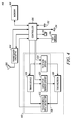
- FIG. 4 depicts a block diagram of an electronic device 400 , such as the mobile communication device 100 of FIG. 1 , in accordance with an embodiment of the present invention.
- the electronic device 400 is depicted as a cellular telephone, the electronic device can be implemented as any wired or wireless electronic device utilizing a touchscreen display user interface such as a pager, a computer, a personal digital assistant, an equipment control device, or the like.
- the electronic device 400 includes the antenna 108 for receiving and transmitting radio frequency (RF) signals.
- the antenna 108 is coupled to transceiver circuitry 404 in a manner familiar to those skilled in the art.
- the transceiver circuitry 404 includes receiver circuitry and transmitter circuitry.
- the receiver circuitry demodulates and decodes received RF signals to derive information therefrom and is coupled to a controller 406 and provides the decoded information to the controller 406 for utilization by the controller 406 in accordance with the function(s) of the electronic device 400 .
- the controller 406 also provides information to the transmitter circuitry of the transceiver circuitry 404 for encoding and modulating the information into RF signals for transmission from the antenna 108 .
- the controller 406 is coupled to a memory 408 which stores data and operational information for use by the controller 406 to perform the functions of the electronic device 400 .
- the controller 406 is also coupled to conventional user interface devices such as any or all of: a microphone 112 , a speaker 114 , a display 110 , and/or functional key inputs 416 .
- the electronic device 400 also includes a touchscreen display system 418 including a touchscreen 420 , a touchscreen input detector 422 , a capacitive sensor driver 423 , a TN stack driver 424 , and a timing device 426 .
- the touchscreen 420 enables the keyless input device 150 ( FIG. 1 ).
- the controller 406 provides control signals to the capacitive sensor driver 423 which, in response to the control signals, provides charging voltages to a capacitive sensor layer of the touchscreen 420 for operation.
- the controller 406 provides control signals to the TN stack driver 424 which, in response to the control signals, provides drive voltages to a TN stack layer of the touchscreen 420 for optical shuttering operation.
- the controller 406 provides additional signals to the touchscreen 420 for other functions such as controlling voltages for operation of a backlight layer of the touchscreen 420 .
- the touchscreen input detector 422 is coupled to the touchscreen 420 for detecting the charge from the capacitive sensing layer thereof and translating the detected charges into user input signals for providing to the controller 406 .
- the timing device 426 is coupled to the touchscreen input detector 422 , the capacitive sensor driver 423 , and the TN stack display driver 424 for control of their operation in accordance with an embodiment of the present invention.
- the timing device 426 , the capacitive sensor driver 423 , and the TN stack driver 424 are typically implemented as separate elements. In accordance with one aspect of the present invention, however, the synergy of the three elements and the ability to coordinate the timing of control signals provided to the capacitive sensing layer 504 , the TN backplane 510 , and the TN segment electrodes 508 (as will be described in accordance with FIGS. 5 and 6 ) can be utilized to incorporate all three elements into a single semiconductor device for advantageously simplifying manufacture of the touchscreen display system 418 and/or of the electronic device 400 . Alternatively, as depicted in FIG.
- the timing device 426 , the touchscreen input detector 422 , the capacitive sensor driver 423 , and the TN stack driver 424 can be implemented as a single semiconductor device 428 .
- the synergy of these four elements and the ability to coordinate the detection of charge within the capacitive sensing layer 504 with the timing of control signals provided to the capacitive sensing layer 504 , the TN backplane 510 , and the TN segment electrodes 508 and the detection of charge within the capacitive sensing layer 504 further simplifies manufacture of the touchscreen display system 418 and/or of the electronic device 400 .
- a cross-sectional view of the touchscreen 420 in accordance with an embodiment of the present invention includes a graphic coverlay layer 502 , a capacitive sensor layer 504 with ITO electrode 505 , a TN stack layer 506 , an electroluminescent (EL) stack layer 516 and a base layer 520 (which may include one or more layers such as a force sensing switch layer and/or a flex base layer) adhered together by adhesive layers applied therebetween.
- the TN stack layer 506 includes two substrates 512 , 514 supporting a TN backplane electrode 510 and TN segment electrodes 508 with TN shutter material 513 sandwiched therebetween.
- the TN shutter material 513 is formulated to have a fast response (or rise) time and a slow decay time such that, in response to application of an electric field to the TN shutter material 513 , liquid crystal material and dichroic dye in the TN shutter material 513 quickly aligns in the direction of the applied field to transmit substantial amounts of incident light while, in response to removal of the electric field, the TN shutter material 213 slowly decays to its noncharged state where the liquid crystal material and the dichroic dye in the TN shutter material 513 randomly align, thereby absorbing most incident light.
- Operation of the touchscreen 420 in accordance with an embodiment of the present invention allows removal of the ITO ground plane layer 218 shown in FIG. 2 , thereby reducing both the thickness of the touchscreen 420 and the cost of its manufacture (e.g., one less process step as well as fewer layers of material and adhesive).
- the ITO layer 218 is not fully light-transmissive (i.e., not fully transparent)
- removal of the ITO layer 218 allows more light from the electroluminescent layer 516 to pass through the optical shuttering TN stack layer 506 and thence to the user, providing sharper and better-defined images 151 , 152 , 153 , 154 , 156 , 157 , 158 , 159 ( FIG. 1 ).
- FIG. 6 illustrates the enhanced operation of the touchscreen 420 in accordance with an embodiment of the present invention.
- the charge 602 from the ITO electrode 505 of the capacitive sensor layer 504 , the voltage 604 of the TN backplane 510 , and the voltages 606 , 608 of first and second portions of the TN segment electrodes 508 are depicted.
- Capacitive sensing during a sensing time interval 610 is performed similarly to conventional operation as described above in accordance with FIG. 3 .
- a charging voltage is provided to the ITO electrode 505 of the capacitive sensor layer 504 for a charging portion 612 of the time interval 610 .
- the charge 602 has two different decay profiles 614 , 616 during a decay period 618 of the time interval 610 depending on whether a user touches the touchscreen 420 .
- the voltages 604 , 606 , 608 supplied to the TN backplane 510 and the TN segment electrodes 508 are switched between a positive voltage, typically about five volts, and zero volts.
- the drive voltages 606 , 608 are provided at a first voltage level of approximately five volts to a predetermined portion of the TN segment electrodes 508 and a remaining portion of the TN segment electrodes 508 , respectively, during a first portion 620 of the sensing time interval 610 and maintained at substantially zero volts during a second portion 622 of the sensing time interval.
- the drive voltages 604 , 608 are provided at approximately five volts to the TN backplane 510 and the predetermined portion of the TN segment electrodes 508 for a first subportion 624 of the first portion 620 of the sensing time interval 610 while the voltage 606 of the remaining portion of the TN segment electrodes 508 is maintained at approximately zero volts.
- the drive voltage 606 of the remaining portion of the TN segment electrodes 508 is provided at approximately five volts, while the voltages 604 , 608 of the TN backplane 510 and the predetermined portion of the TN segment electrodes 508 is switched to approximately zero volts.
- the predetermined portion of the TN segment electrodes 508 are “off” 610 and the remaining portion of the TN segment electrodes 508 are “on” during the sensing time interval 610 .
- a simple variation is to predetermine the “on” TN segment electrodes and reverse the timing of the applied voltages.
- Operation in accordance with an embodiment allows optical shuttering operation with drive voltages 604 , 606 , 608 provided only during the first portion 612 of the sensing time interval 610 while a drive voltage 602 is also being provided to the capacitive sensor layer 504 simultaneously during a charging portion 612 of the sensing time interval 610 .
- the semiconductor device 428 can be utilized for providing the voltages to generate the charge 602 as well as the voltages 604 , 606 , 608 .
- the drive voltages 604 , 606 , 608 provided to the TN backplane 510 and the TN segment electrodes 508 are maintained near zero volts throughout the second portion 622 of the sensing time interval 610 which coincides with the decay period 618 thereby decreasing electrical noise during the decay period 618 and increasing the SNR of the measured charge 602 during the crucial time that the decay curve profiles 614 or 616 are being detected by the touchscreen input detector 422 .
- the timing device 426 is configured to provide timing for the TN stack driver 424 to provide the drive voltages 604 , 606 , 608 and for the capacitive sensor driver 423 to provide the charge to the ITO electrode 505 of the capacitive sensor layer 504 in accordance with an embodiment of the present invention as well as providing timing for the touchscreen input detector 422 to detect the decay curve profile 614 , 616 during the decay period 618 .
Abstract
Description
Claims (19)
Priority Applications (3)
| Application Number | Priority Date | Filing Date | Title |
|---|---|---|---|
| US11/611,970 US7755615B2 (en) | 2006-12-18 | 2006-12-18 | Optical shuttered touchscreen and method therefor |
| KR1020097015073A KR101100506B1 (en) | 2006-12-18 | 2007-08-04 | Optical shuttered touchscreen and method therefor |
| PCT/US2007/074916 WO2008076474A2 (en) | 2006-12-18 | 2007-08-04 | Optical shuttered touchscreen and method therefor |
Applications Claiming Priority (1)
| Application Number | Priority Date | Filing Date | Title |
|---|---|---|---|
| US11/611,970 US7755615B2 (en) | 2006-12-18 | 2006-12-18 | Optical shuttered touchscreen and method therefor |
Publications (2)
| Publication Number | Publication Date |
|---|---|
| US20080143689A1 US20080143689A1 (en) | 2008-06-19 |
| US7755615B2 true US7755615B2 (en) | 2010-07-13 |
Family
ID=39438244
Family Applications (1)
| Application Number | Title | Priority Date | Filing Date |
|---|---|---|---|
| US11/611,970 Active 2029-05-12 US7755615B2 (en) | 2006-12-18 | 2006-12-18 | Optical shuttered touchscreen and method therefor |
Country Status (3)
| Country | Link |
|---|---|
| US (1) | US7755615B2 (en) |
| KR (1) | KR101100506B1 (en) |
| WO (1) | WO2008076474A2 (en) |
Cited By (2)
| Publication number | Priority date | Publication date | Assignee | Title |
|---|---|---|---|---|
| US20090066643A1 (en) * | 2007-09-07 | 2009-03-12 | Samsung Electronics Co., Ltd | Touch screen panel to input multi-dimension values and method for controlling touch screen panel |
| US20120242614A1 (en) * | 2009-07-29 | 2012-09-27 | Ferreira Tiago Jose Monteiro Baptista Cabral | Electrochromic Touchscreen |
Families Citing this family (21)
| Publication number | Priority date | Publication date | Assignee | Title |
|---|---|---|---|---|
| TWI459249B (en) * | 2007-07-17 | 2014-11-01 | Elan Microelectronics | Light emitting touch pad and controlling system having the same |
| US7742125B2 (en) * | 2007-08-24 | 2010-06-22 | World Properties, Inc. | Light switch having plural shutters |
| US9665197B2 (en) * | 2008-01-30 | 2017-05-30 | Nokia Technologies Oy | Apparatus and method for enabling user input |
| CA2728410C (en) * | 2008-06-20 | 2014-05-06 | Mattel, Inc. | Capacitive touchpad and toy incorporating the same |
| KR101667801B1 (en) * | 2009-06-19 | 2016-10-20 | 삼성전자주식회사 | Touch panel and electronic device including the touch panel |
| KR101658991B1 (en) * | 2009-06-19 | 2016-09-22 | 삼성전자주식회사 | Touch panel and electronic device including the touch panel |
| KR101616875B1 (en) * | 2010-01-07 | 2016-05-02 | 삼성전자주식회사 | Touch panel and electronic device including the touch panel |
| KR101631892B1 (en) * | 2010-01-28 | 2016-06-21 | 삼성전자주식회사 | Touch panel and electronic device including the touch panel |
| KR101710523B1 (en) * | 2010-03-22 | 2017-02-27 | 삼성전자주식회사 | Touch panel and electronic device including the touch panel |
| KR101661728B1 (en) | 2010-05-11 | 2016-10-04 | 삼성전자주식회사 | User's input apparatus and electronic device including the user's input apparatus |
| US10831317B2 (en) * | 2010-08-20 | 2020-11-10 | Neodrón Limited | Electronic ink touch sensitive display |
| KR101809191B1 (en) | 2010-10-11 | 2018-01-18 | 삼성전자주식회사 | Touch panel |
| KR101735715B1 (en) | 2010-11-23 | 2017-05-15 | 삼성전자주식회사 | Input sensing circuit and touch panel including the input sensing circuit |
| KR101784436B1 (en) | 2011-04-18 | 2017-10-11 | 삼성전자주식회사 | Touch panel and driving device for the touch panel |
| TWI531936B (en) * | 2011-10-24 | 2016-05-01 | 友達光電股份有限公司 | Touch display device |
| US10091556B1 (en) * | 2012-12-12 | 2018-10-02 | Imdb.Com, Inc. | Relating items to objects detected in media |
| US9244559B2 (en) | 2012-12-14 | 2016-01-26 | Atmel Corporation | Integrated pixel display and touch sensor |
| CN103035209B (en) * | 2012-12-24 | 2015-09-02 | 东莞宇龙通信科技有限公司 | Terminal and screen backlight control method |
| US10528250B2 (en) | 2014-02-21 | 2020-01-07 | Groupon, Inc. | Method and system for facilitating consumer interactions with promotions |
| US11653052B2 (en) * | 2020-10-26 | 2023-05-16 | Genetec Inc. | Systems and methods for producing a privacy-protected video clip |
| WO2023129266A1 (en) * | 2021-12-28 | 2023-07-06 | The Adt Security Corporation | Video rights management for an in-cabin monitoring system |
Citations (12)
| Publication number | Priority date | Publication date | Assignee | Title |
|---|---|---|---|---|
| US5606346A (en) | 1992-12-22 | 1997-02-25 | Matsushita Electric Industrial Co., Ltd. | Coordinate input device |
| EP0802476A2 (en) | 1996-04-16 | 1997-10-22 | SHARP Corporation | Pen input apparatus and pen input method for detecting approach of pen to display integrated tablet by controlling lighting of back light |
| US5777596A (en) * | 1995-11-13 | 1998-07-07 | Symbios, Inc. | Touch sensitive flat panel display |
| GB2348039A (en) | 1999-03-17 | 2000-09-20 | Motorola Inc | Display with aligned optical shutter and backlight cells |
| US6788282B2 (en) | 2002-02-21 | 2004-09-07 | Seiko Epson Corporation | Driving method for electro-optical device, driving circuit therefor, electro-optical device, and electronic apparatus |
| US6822640B2 (en) * | 2001-04-10 | 2004-11-23 | Hewlett-Packard Development Company, L.P. | Illuminated touch pad |
| US20050122284A1 (en) | 2003-11-25 | 2005-06-09 | E Ink Corporation | Electro-optic displays, and methods for driving same |
| US20050162410A1 (en) * | 2002-03-15 | 2005-07-28 | Koninklijke Philips Electronics N.V. | Touch sensitive display device |
| US20050162411A1 (en) * | 2002-06-07 | 2005-07-28 | Berkel Van Cornelis | Input system |
| US6940484B2 (en) | 2000-07-21 | 2005-09-06 | Seiko Epson Corporation | Systems and methods for driving a display device |
| US20050280635A1 (en) * | 2004-06-22 | 2005-12-22 | Shoji Hinata | Input device, electro-optical device, electronic apparatus, method of manufacturing input device, and method of manufacturing electro-optical device |
| US7545343B2 (en) * | 2004-01-28 | 2009-06-09 | Sharp Kabushiki Kaisha | Display device |
Family Cites Families (1)
| Publication number | Priority date | Publication date | Assignee | Title |
|---|---|---|---|---|
| JP2003091365A (en) | 2001-09-19 | 2003-03-28 | Sharp Corp | Coordinate input device |
-
2006
- 2006-12-18 US US11/611,970 patent/US7755615B2/en active Active
-
2007
- 2007-08-04 KR KR1020097015073A patent/KR101100506B1/en active IP Right Grant
- 2007-08-04 WO PCT/US2007/074916 patent/WO2008076474A2/en active Application Filing
Patent Citations (14)
| Publication number | Priority date | Publication date | Assignee | Title |
|---|---|---|---|---|
| US5606346A (en) | 1992-12-22 | 1997-02-25 | Matsushita Electric Industrial Co., Ltd. | Coordinate input device |
| US5777596A (en) * | 1995-11-13 | 1998-07-07 | Symbios, Inc. | Touch sensitive flat panel display |
| EP0802476A2 (en) | 1996-04-16 | 1997-10-22 | SHARP Corporation | Pen input apparatus and pen input method for detecting approach of pen to display integrated tablet by controlling lighting of back light |
| US5894304A (en) | 1996-04-16 | 1999-04-13 | Sharp Kabushiki Kaisha | Pen input apparatus and pen input method for detecting approach of pen to display integrated tablet by controlling lighting of back light |
| US6842170B1 (en) * | 1999-03-17 | 2005-01-11 | Motorola, Inc. | Display with aligned optical shutter and backlight cells applicable for use with a touchscreen |
| GB2348039A (en) | 1999-03-17 | 2000-09-20 | Motorola Inc | Display with aligned optical shutter and backlight cells |
| US6940484B2 (en) | 2000-07-21 | 2005-09-06 | Seiko Epson Corporation | Systems and methods for driving a display device |
| US6822640B2 (en) * | 2001-04-10 | 2004-11-23 | Hewlett-Packard Development Company, L.P. | Illuminated touch pad |
| US6788282B2 (en) | 2002-02-21 | 2004-09-07 | Seiko Epson Corporation | Driving method for electro-optical device, driving circuit therefor, electro-optical device, and electronic apparatus |
| US20050162410A1 (en) * | 2002-03-15 | 2005-07-28 | Koninklijke Philips Electronics N.V. | Touch sensitive display device |
| US20050162411A1 (en) * | 2002-06-07 | 2005-07-28 | Berkel Van Cornelis | Input system |
| US20050122284A1 (en) | 2003-11-25 | 2005-06-09 | E Ink Corporation | Electro-optic displays, and methods for driving same |
| US7545343B2 (en) * | 2004-01-28 | 2009-06-09 | Sharp Kabushiki Kaisha | Display device |
| US20050280635A1 (en) * | 2004-06-22 | 2005-12-22 | Shoji Hinata | Input device, electro-optical device, electronic apparatus, method of manufacturing input device, and method of manufacturing electro-optical device |
Non-Patent Citations (1)
| Title |
|---|
| International Search Report PCT/US2007/074916 dated Jun. 11, 2008. |
Cited By (4)
| Publication number | Priority date | Publication date | Assignee | Title |
|---|---|---|---|---|
| US20090066643A1 (en) * | 2007-09-07 | 2009-03-12 | Samsung Electronics Co., Ltd | Touch screen panel to input multi-dimension values and method for controlling touch screen panel |
| US8812992B2 (en) * | 2007-09-07 | 2014-08-19 | Samsung Electronics Co., Ltd. | Touch screen panel to input multi-dimension values and method for controlling touch screen panel |
| US20120242614A1 (en) * | 2009-07-29 | 2012-09-27 | Ferreira Tiago Jose Monteiro Baptista Cabral | Electrochromic Touchscreen |
| US8907918B2 (en) * | 2009-07-29 | 2014-12-09 | Yd Ynvisible, S.A. | Electrochromic touchscreen |
Also Published As
| Publication number | Publication date |
|---|---|
| KR101100506B1 (en) | 2011-12-29 |
| WO2008076474A3 (en) | 2008-08-21 |
| WO2008076474A2 (en) | 2008-06-26 |
| US20080143689A1 (en) | 2008-06-19 |
| KR20090101940A (en) | 2009-09-29 |
Similar Documents
| Publication | Publication Date | Title |
|---|---|---|
| US7755615B2 (en) | Optical shuttered touchscreen and method therefor | |
| US11009733B2 (en) | Detection device and display device | |
| US8952913B2 (en) | Display device and driving method thereof | |
| KR100955339B1 (en) | Touch and proximity sensible display panel, display device and Touch and proximity sensing method using the same | |
| CN103576360B (en) | Liquid crystal indicator with touch sensing device and electronics | |
| CN102375637B (en) | Display device and method, drive circuit and electronic equipment | |
| US9035900B2 (en) | Touch detector and method of driving the same, display with touch detection function, and electronic unit having plural different drive electrodes | |
| CN1149434C (en) | Display device with alignment light valve and adapted for back light unit of touch screen | |
| US8203536B2 (en) | Display unit | |
| EP2163970A2 (en) | Adaptable user interface and mechanism for a portable electronic device | |
| CN109190592B (en) | LCD display device and electronic equipment | |
| US20110216043A1 (en) | Electronic device and electronic system | |
| KR20090113371A (en) | Multimodal adaptive user interface for a portable electronic device | |
| CN103049126A (en) | Display unit, display method, and electronic system | |
| KR20110100377A (en) | Liquid crystal display panel with a built-in touch screen, and liquid crystal display device having the same | |
| WO2009064601A1 (en) | Mobile electronic device having capacitive sensor with reduced visibility isolation areas and corresponding method | |
| JP2024056788A (en) | Display Panel | |
| US7729106B2 (en) | Smudge removal from electronic device displays | |
| US20150234525A1 (en) | Powered card with touch display | |
| CN105138179B (en) | Full-embedded type touch screen and mobile device | |
| EP2115556A1 (en) | Adaptable user interface and mechanism for a portable electronic device | |
| JP2009116224A (en) | Touch panel integrated type liquid crystal display device, touch detecting method and portable terminal | |
| CN103885222A (en) | Driving method for touch display device and touch display device | |
| KR101957150B1 (en) | Haptic touch screen and method for driving the same | |
| KR20170079988A (en) | Electronic device and method for touch sensing the same |
Legal Events
| Date | Code | Title | Description |
|---|---|---|---|
| AS | Assignment |
Owner name: MOTOROLA, INC., ILLINOIS Free format text: ASSIGNMENT OF ASSIGNORS INTEREST;ASSIGNORS:FOO, KEN K;KAEHLER, JOHN W.;YU, PINKY;REEL/FRAME:018842/0820 Effective date: 20061212 |
|
| STCF | Information on status: patent grant |
Free format text: PATENTED CASE |
|
| AS | Assignment |
Owner name: MOTOROLA MOBILITY, INC, ILLINOIS Free format text: ASSIGNMENT OF ASSIGNORS INTEREST;ASSIGNOR:MOTOROLA, INC;REEL/FRAME:025673/0558 Effective date: 20100731 |
|
| AS | Assignment |
Owner name: MOTOROLA MOBILITY LLC, ILLINOIS Free format text: CHANGE OF NAME;ASSIGNOR:MOTOROLA MOBILITY, INC.;REEL/FRAME:029216/0282 Effective date: 20120622 |
|
| FPAY | Fee payment |
Year of fee payment: 4 |
|
| AS | Assignment |
Owner name: GOOGLE TECHNOLOGY HOLDINGS LLC, CALIFORNIA Free format text: ASSIGNMENT OF ASSIGNORS INTEREST;ASSIGNOR:MOTOROLA MOBILITY LLC;REEL/FRAME:034450/0001 Effective date: 20141028 |
|
| MAFP | Maintenance fee payment |
Free format text: PAYMENT OF MAINTENANCE FEE, 8TH YEAR, LARGE ENTITY (ORIGINAL EVENT CODE: M1552) Year of fee payment: 8 |
|
| MAFP | Maintenance fee payment |
Free format text: PAYMENT OF MAINTENANCE FEE, 12TH YEAR, LARGE ENTITY (ORIGINAL EVENT CODE: M1553); ENTITY STATUS OF PATENT OWNER: LARGE ENTITY Year of fee payment: 12 |