US7741644B2 - Semiconductor device having stacked transistors - Google Patents

Semiconductor device having stacked transistors Download PDF

Info

Publication number
US7741644B2
US7741644B2 US11/672,875 US67287507A US7741644B2 US 7741644 B2 US7741644 B2 US 7741644B2 US 67287507 A US67287507 A US 67287507A US 7741644 B2 US7741644 B2 US 7741644B2
Authority
US
United States
Prior art keywords
layer
semiconductor layer
semiconductor device
semiconductor
interlayer insulation
Prior art date
Legal status (The legal status is an assumption and is not a legal conclusion. Google has not performed a legal analysis and makes no representation as to the accuracy of the status listed.)
Active, expires
Application number
US11/672,875
Other versions
US20070181953A1 (en
Inventor
Gyu-Ho LYU
Seug-Gyu KIM
Current Assignee (The listed assignees may be inaccurate. Google has not performed a legal analysis and makes no representation or warranty as to the accuracy of the list.)
Samsung Electronics Co Ltd
Original Assignee
Samsung Electronics Co Ltd
Priority date (The priority date is an assumption and is not a legal conclusion. Google has not performed a legal analysis and makes no representation as to the accuracy of the date listed.)
Filing date
Publication date
Application filed by Samsung Electronics Co Ltd filed Critical Samsung Electronics Co Ltd
Assigned to SAMSUNG ELECTRONICS CO., LTD. reassignment SAMSUNG ELECTRONICS CO., LTD. ASSIGNMENT OF ASSIGNORS INTEREST (SEE DOCUMENT FOR DETAILS). Assignors: KIM, SEUG-GYU, LYU, GYU-HO
Publication of US20070181953A1 publication Critical patent/US20070181953A1/en
Application granted granted Critical
Publication of US7741644B2 publication Critical patent/US7741644B2/en
Active legal-status Critical Current
Adjusted expiration legal-status Critical

Links

Images

Classifications

    • HELECTRICITY
    • H01ELECTRIC ELEMENTS
    • H01LSEMICONDUCTOR DEVICES NOT COVERED BY CLASS H10
    • H01L27/00Devices consisting of a plurality of semiconductor or other solid-state components formed in or on a common substrate
    • H01L27/02Devices consisting of a plurality of semiconductor or other solid-state components formed in or on a common substrate including semiconductor components specially adapted for rectifying, oscillating, amplifying or switching and having potential barriers; including integrated passive circuit elements having potential barriers
    • H01L27/04Devices consisting of a plurality of semiconductor or other solid-state components formed in or on a common substrate including semiconductor components specially adapted for rectifying, oscillating, amplifying or switching and having potential barriers; including integrated passive circuit elements having potential barriers the substrate being a semiconductor body
    • H01L27/06Devices consisting of a plurality of semiconductor or other solid-state components formed in or on a common substrate including semiconductor components specially adapted for rectifying, oscillating, amplifying or switching and having potential barriers; including integrated passive circuit elements having potential barriers the substrate being a semiconductor body including a plurality of individual components in a non-repetitive configuration
    • H01L27/0688Integrated circuits having a three-dimensional layout
    • FMECHANICAL ENGINEERING; LIGHTING; HEATING; WEAPONS; BLASTING
    • F24HEATING; RANGES; VENTILATING
    • F24FAIR-CONDITIONING; AIR-HUMIDIFICATION; VENTILATION; USE OF AIR CURRENTS FOR SCREENING
    • F24F1/00Room units for air-conditioning, e.g. separate or self-contained units or units receiving primary air from a central station
    • F24F1/06Separate outdoor units, e.g. outdoor unit to be linked to a separate room comprising a compressor and a heat exchanger
    • F24F1/26Refrigerant piping
    • F24F1/34Protection means thereof, e.g. covers for refrigerant pipes
    • FMECHANICAL ENGINEERING; LIGHTING; HEATING; WEAPONS; BLASTING
    • F24HEATING; RANGES; VENTILATING
    • F24FAIR-CONDITIONING; AIR-HUMIDIFICATION; VENTILATION; USE OF AIR CURRENTS FOR SCREENING
    • F24F13/00Details common to, or for air-conditioning, air-humidification, ventilation or use of air currents for screening
    • F24F13/20Casings or covers
    • HELECTRICITY
    • H01ELECTRIC ELEMENTS
    • H01LSEMICONDUCTOR DEVICES NOT COVERED BY CLASS H10
    • H01L21/00Processes or apparatus adapted for the manufacture or treatment of semiconductor or solid state devices or of parts thereof
    • H01L21/70Manufacture or treatment of devices consisting of a plurality of solid state components formed in or on a common substrate or of parts thereof; Manufacture of integrated circuit devices or of parts thereof
    • H01L21/77Manufacture or treatment of devices consisting of a plurality of solid state components or integrated circuits formed in, or on, a common substrate
    • H01L21/78Manufacture or treatment of devices consisting of a plurality of solid state components or integrated circuits formed in, or on, a common substrate with subsequent division of the substrate into plural individual devices
    • H01L21/82Manufacture or treatment of devices consisting of a plurality of solid state components or integrated circuits formed in, or on, a common substrate with subsequent division of the substrate into plural individual devices to produce devices, e.g. integrated circuits, each consisting of a plurality of components
    • H01L21/822Manufacture or treatment of devices consisting of a plurality of solid state components or integrated circuits formed in, or on, a common substrate with subsequent division of the substrate into plural individual devices to produce devices, e.g. integrated circuits, each consisting of a plurality of components the substrate being a semiconductor, using silicon technology
    • H01L21/8221Three dimensional integrated circuits stacked in different levels
    • HELECTRICITY
    • H10SEMICONDUCTOR DEVICES; ELECTRIC SOLID-STATE DEVICES NOT OTHERWISE PROVIDED FOR
    • H10BELECTRONIC MEMORY DEVICES
    • H10B10/00Static random access memory [SRAM] devices
    • HELECTRICITY
    • H10SEMICONDUCTOR DEVICES; ELECTRIC SOLID-STATE DEVICES NOT OTHERWISE PROVIDED FOR
    • H10BELECTRONIC MEMORY DEVICES
    • H10B10/00Static random access memory [SRAM] devices
    • H10B10/12Static random access memory [SRAM] devices comprising a MOSFET load element
    • H10B10/125Static random access memory [SRAM] devices comprising a MOSFET load element the MOSFET being a thin film transistor [TFT]

Definitions

  • Embodiments disclosed herein relate generally to semiconductor devices and, more particularly, to a semiconductor device having stacked transistors and a method of forming the same.
  • Most recent electronic appliances include semiconductor devices that include electronic elements such as a transistor, a resistor, and a capacitor.
  • the electronic elements are designed and manufactured to perform expected functions and are then integrated together on a semiconductor substrate.
  • the electronic appliances such as a computer and a digital camera include semiconductor devices such as a memory chip for storing information and a processing chip for controlling information.
  • the memory chip and the processing chip include electronic elements integrated on a semiconductor substrate.
  • semiconductor devices need to be more highly integrated to satisfy consumers with an excellent performance and a reasonable price.
  • electronic elements constituting a semiconductor device are miniaturized to achieve high integration.
  • a developing speed of miniaturizing the electronic elements is under certain restriction. Accordingly, a new semiconductor device manufacturing method for overcoming the miniaturization limitation is required to achieve the desired integration of the semiconductor device.
  • FIG. 1 is a sectional view of a conventional semiconductor device having stacked transistors.
  • a conventional semiconductor device 10 includes a plurality of first transistors 12 on a semiconductor substrate 11 having a device isolation layer 11 ′.
  • the first transistor 12 includes source/drain regions 12 ′.
  • a first interlayer insulation layer 13 covers the first transistors 12 on the semiconductor substrate 11 .
  • a semiconductor layer 14 formed from a seed plug 13 ′ is on the first interlayer insulation layer 13 .
  • Second transistors 15 are provided on the semiconductor layer 14 , and a second interlayer insulation layer 16 is provided on the second transistors 15 .
  • the second transistor 15 includes source/drain regions 14 ′.
  • a conducting column 17 penetrates the source/drain regions 14 ′ of the semiconductor layer 14 and the second and first interlayer insulation layers 16 and 13 to contact the semiconductor substrate 11 .
  • the semiconductor substrate 11 is electrically connected to the second transistors 15 via the semiconductor layer 14 and the conducting column 17 .
  • the semiconductor layer 14 is thinly formed to reduce a leakage current of the second transistors 15 .
  • a contact area “A” between the conducting column 17 and the source/drain regions 14 ′ of the semiconductor layer 14 decreases. Therefore, contact resistance increases and semiconductor device characters deteriorate.
  • Embodiments exemplary described herein provide a highly integrated semiconductor device having improved electric characteristics.
  • Embodiments exemplary described also provide a method of forming a semiconductor device to overcome a technical limitation for miniaturization and increase the degree of integration.
  • One embodiment described herein can be exemplarily characterized as a semiconductor device that includes a first semiconductor layer; a first interlayer insulation layer covering the first semiconductor layer; a second semiconductor layer on the first interlayer insulation layer, the second semiconductor layer comprising a source region, a drain region and a channel region interposed between the source and drain regions; and a gate pattern on the channel region, wherein at least one of the source and drain regions comprises an elevated layer, wherein a top surface of the elevated layer is above a top surface of the channel region.
  • Another embodiment described herein can be exemplarily characterized as a method of forming a semiconductor device that includes forming a first interlayer insulation layer covering a first semiconductor layer; forming a second semiconductor layer on the first interlayer insulation layer; forming a source region, a drain region and a channel region interposed between the source and drain regions within the second semiconductor layer; forming a gate pattern on the channel region; and forming an elevated layer on at least one of the source and drain regions, wherein a top surface of the elevated layer is above a top surface of the channel region.
  • FIG. 1 is a sectional view of a conventional semiconductor device having stacked transistors
  • FIG. 2 is a sectional view of one embodiment of a semiconductor device having stacked transistors
  • FIGS. 3A through 3F are sectional views illustrating an exemplary method of forming a semiconductor device having stacked transistors.
  • FIGS. 4A and 4B are sectional views of exemplary applications of the semiconductor device described with respect to FIGS. 2 and 3A through 3 F.
  • FIG. 2 is a sectional view of one embodiment of a semiconductor device 100 having stacked transistors.
  • the semiconductor device 100 is formed on a first semiconductor layer 110 having an active region 115 that is divided by a device isolation layer 113 .
  • the first semiconductor layer 110 may be a single crystal semiconductor substrate, or a silicon-on-insulator (SOI) substrate having a semiconductor layer that is formed interposing an insulation layer therebetween.
  • the first semiconductor layer 110 may contain a first conductivity-type impurity (e.g., p-type impurity ions).
  • a plurality of first transistors 120 may be disposed on the first semiconductor layer 110 .
  • the first transistor 120 includes a gate insulation layer 122 , a gate electrode pattern 124 , a capping pattern 127 , and a first sidewall spacer 126 .
  • the gate insulation layer 122 may include a material such as, for example, thermal silicon oxide and the gate electrode pattern 124 may include a material such as, for example, polysilicon containing a second conductivity-type impurity (e.g., n-type impurity ions) opposite to the first conductivity-type impurity.
  • the capping pattern 127 may include a material such as, for example, silicon oxide or silicon nitride.
  • the first sidewall spacer 126 may include a material such as, for example, silicon oxide. Impurity regions 128 for source and drain regions are disposed on both sides of the gate electrode pattern 124 .
  • the impurity regions 128 may contain the second conductivity-type impurity (e.g., n-type impurity ions) opposite to the first conductivity-type impurity.
  • the impurity regions 128 may be include a low-concentration impurity region 128 a and a high-concentration impurity region 128 b over the low-concentration impurity region 128 a.
  • a first interlayer insulation layer 130 covers the first transistors 120 on the first semiconductor layer 110 .
  • the first interlayer insulation layer 130 include a material such as, for example, silicon oxide.
  • An etch stop layer 132 may additionally be formed under the first interlayer insulation layer 130 to, for example, prevent the first semiconductor layer 110 from being damaged during a subsequent etching process for contact hole formation.
  • the etch stop layer 132 may include an insulation material having a lower etch rate than that of the first interlayer insulation layer 110 such as, for example, silicon nitride or silicon oxide nitride.
  • a second semiconductor layer 140 is provided on the first interlayer insulation layer 130 .
  • the second semiconductor layer 140 includes source/drain regions 144 and 146 , and a channel region 142 interposed between the source region 144 and the drain region 146 .
  • An epitaxial seed plug 135 is disposed between the first semiconductor layer 110 and the second semiconductor layer 140 to penetrate the first interlayer insulation layer 130 .
  • the epitaxial seed plug 135 may be grown from the single-crystal first semiconductor layer 110 using a selective epitaxial growth (SEG) method and may include silicon doped with the second conductivity-type impurity ions.
  • the second semiconductor layer 140 may be epitaxially grown from the epitaxial seed plug 135 , and may include a silicon layer doped with the first conductivity-type impurity ions.
  • Second transistors 150 are disposed on the second semiconductor layer 140 .
  • the second transistor 150 includes a gate pattern 154 having a gate insulation layer 152 interposed on the channel region 142 , a capping pattern 156 , and a second sidewall spacer 158 .
  • the gate insulation layer 152 may include a material such as, for example, thermal silicon oxide.
  • the gate electrode 154 may include a material such as, for example, silicon containing the second conductivity-type (e.g., n-type impurity ions) opposite to the first conductivity-type.
  • the capping pattern 156 may include a material such as, for example, silicon oxide or silicon nitride and the second sidewall spacer 158 may include a material such as, for example, silicon oxide.
  • Impurity regions 144 and 146 for source/drain regions are disposed on both sides of the gate pattern 154 .
  • the impurity regions 144 and 146 may contain the second conductivity-type (e.g., n-type impurity ions).
  • the impurity regions 144 and 146 include low-concentration impurity regions 144 a and 146 a , and high-concentration impurity regions 144 b and 146 b over the low-concentration impurity regions 144 a and 146 a .
  • the low-concentration impurity regions 144 a and 146 a may extend to the bottom of the second semiconductor layer 140 .
  • the high-concentration impurity regions 144 b and 146 b may be spaced apart from the bottom portion of the second semiconductor layer 140 and may be formed to extend to the top portion of the second semiconductor layer 140 . Since the high-concentration impurity regions 144 b and 146 b are only formed on the top portion of the second semiconductor layer 140 and do not extend to the bottom portion of the second semiconductor layer 140 , shallow junctions can be achieved.
  • An elevated layer 140 a (i.e., a first elevated layer) having a top surface that is above the channel region 142 is disposed on the top portion of at least one of the impurity regions 144 and 146 .
  • the elevated layer 140 a is adjacent to a second sidewall spacer 158 of the second transistor 150 and is self-aligned thereto.
  • the elevated layer 140 a may be epitaxially grown from the second semiconductor layer 140 adjacent to the second sidewall spacers 158 using the SEG method.
  • the elevated layer 140 a may be a portion of the high-concentration impurity region doped with impurity ions of a conductivity-type identical to that of the impurity for the source/drain regions. That is, the high-concentration impurity regions 144 b and 146 b may include the top portion of the second semiconductor layer 140 and the elevated layer 140 a.
  • a second interlayer insulation layer 160 covers the second transistors 150 on the second semiconductor layer 140 .
  • a first conducting column 170 penetrates the second interlayer insulation layer 160 , the elevated layer 140 a , the second semiconductor layer 140 , and the first interlayer insulation layer 130 and is connected to the first semiconductor layer 110 . Accordingly, the first semiconductor layer 110 is electrically connected to the second semiconductor layer 140 through the first conducting column 170 . The side of the first conducting column 170 contacts the elevated layer 140 a and the second semiconductor layer 140 .
  • a second conducting column 180 may penetrate the second interlayer insulation layer 160 to connect to the source region or the drain region including the elevated layer 140 a . Accordingly, a lower portion of the second conducting column 180 contacts the elevated layer 140 a and the second semiconductor layer 140 .
  • the first and second conducting columns 170 and 180 may include a barrier layer (e.g., a barrier metal layer) and a conductor material (e.g., a metal material) surrounded by a barrier layer.
  • the barrier layer may include a material such as, for example, titanium or titanium nitride, and the conductor material may include a material such as, for example, tungsten.
  • the first and second conducting columns 170 and 180 contact the elevated layer 140 a and the impurity regions 144 and 146 of the second semiconductor layer 140 at the “B” regions. Due to the presence of the elevated layer 140 a , the contact area at the “B” regions is greater than a contact area at the “A” region shown in FIG. 1 . Accordingly, an electrical contact resistance can be reduced relative to the electrical contact resistance of the device shown in FIG. 1 . Further, the leakage current of the second transistor 150 can be decreased by reducing the thickness of the second semiconductor layer 140 , and thus the thickness of the channel region 142 .
  • FIGS. 3A through 3F are sectional views illustrating an exemplary method of forming a semiconductor device having stacked transistors.
  • a device isolation layer 113 is formed on the first semiconductor layer 110 , and an active region 115 is defined by the device isolation layer 113 .
  • the first semiconductor layer 110 may be a single crystal semiconductor substrate, or a SOI substrate having a semiconductor layer that is formed interposing an insulation layer on the semiconductor substrate.
  • the first semiconductor layer 110 may contain a first conductivity-type impurity (e.g., p-type impurity ions).
  • a plurality of first transistors 120 are formed on the active region 115 of the first semiconductor layer 110 .
  • the first transistor 120 includes a gate insulation layer 122 , a gate electrode pattern 124 , a capping pattern 127 , and first sidewall spacers 126 .
  • the gate insulation layer 122 is disposed on the first semiconductor layer 110 followed by the formation and patterning of a polysilicon layer (i.e., a gate conductor layer) and a capping layer such that the gate electrode pattern 124 and the capping pattern 127 are thereby formed.
  • the polysilicon layer may contain the second conductivity-type impurity.
  • the capping layer protects the polysilicon layer and may include a material such as, for example, silicon oxide or silicon nitride.
  • the gate insulation layer 122 may include a material such as, for example, silicon oxide formed, for example, by subjecting the first semiconductor layer 110 to a thermal oxidation process.
  • first concentration impurity ions of the second conductivity-type are implanted to form low-concentration source/drain regions 128 a .
  • first sidewall spacers 126 are formed on both sidewalls of the gate electrode pattern 124 and the capping pattern 127 .
  • the first sidewall spacers 126 include a silicon oxide material that has been deposited over the gate electrode pattern 124 and the capping pattern 127 and anisotropically etched.
  • the second conductivity-type impurity ions having a second concentration higher than the first concentration are implanted to form high-concentration source/drain regions 128 b on the both sides of the gate electrode pattern 124 .
  • the source/drain regions 128 include a low-concentration impurity region 128 a and a high-concentration impurity region 128 b formed in the low-concentration impurity region 128 a.
  • a first interlayer insulation layer 130 is formed to cover the first transistors 120 on the first semiconductor layer 110 .
  • the first interlayer insulation layer 130 may include a material such as, for example, silicon oxide formed according to a high density plasma deposition (HDP) process, a borophosphosilicate glass (BPSG) process, or a plasma enhanced tetra-ethyl-ortho-silicate (PE-TEOS) process, and also may be planarized for transistor stacking.
  • An etch stop layer 132 may be formed between the first interlayer insulation layer 130 and the first semiconductor layer 110 .
  • the etch stop layer 132 prevents the first semiconductor layer 110 from being damaged during a subsequent etching process for contact hole formation.
  • the etch stop layer 132 may include an insulation material having a lower etch rate than that of the first interlayer insulation layer 110 such as, for example, silicon nitride or silicon oxide nitride.
  • the first interlayer insulation layer 130 is patterned using a photoresist pattern (not shown) to form a seed contact hole 133 exposing a predetermined region of the first semiconductor layer 110 (e.g., a portion of a source/drain region 128 ).
  • An epitaxial seed plug 135 may then be formed to fill the seed contact hole 133 .
  • the filling process may be performed according to a selective epitaxial growth (SEG) method.
  • SEG selective epitaxial growth
  • the region of the first semiconductor layer 110 exposed by the seed contact hole 133 is used as a seed layer.
  • 3B illustrates the epitaxial seed plug 135 as substantially completely filling the seed contact hole 133 , it will be appreciated that the epitaxial seed plug 135 may not completely fill the seed contact hole 133 .
  • a single-crystal silicon layer may be grown at approximately 800° C. using a process gas including DCS and HCl.
  • a thermal treatment process may be additionally performed to stabilize the grown single-crystal silicon layer.
  • crystal growth occurs only on the seed layer.
  • a second semiconductor layer 140 is formed on the epitaxial seed plug 135 .
  • Various methods may be employed to form the second semiconductor layer 140 .
  • a SEG process is employed to form the second semiconductor layer 140 formed using the epitaxial seed plug 135 as a seed layer. As shown, the SEG process ensures that the second semiconductor layer 140 sufficiently cover the top surface of the first interlayer insulation layer 130 .
  • the second semiconductor layer 140 is planarized using a chemical mechanical polishing (CMP) process.
  • CMP chemical mechanical polishing
  • the second semiconductor layer 140 is patterned to have a predetermined pattern. In one embodiment, the second semiconductor layer 140 may be patterned to form a body layer having transistors.
  • the second semiconductor layer 140 may be formed by employing various epitaxial process (other than SEG) such as solid phase epitaxy (SPE), liquid phase epitaxy (LPE), vapor phase epitaxy (VPE), or the like or combinations thereof.
  • SPE solid phase epitaxy
  • LPE liquid phase epitaxy
  • VPE vapor phase epitaxy
  • an amorphous or polycrystalline silicon layer contacting the epitaxial seed plug 135 is formed on the first interlayer insulation layer 130 and then a crystallization process (e.g., a heat treatment process) is performed to convert the amorphous or polycrystalline silicon layer into a single-crystal silicon layer.
  • a crystallization process e.g., a heat treatment process
  • an amorphous or polycrystalline silicon layer contacting the epitaxial seed plug 135 is formed on the first interlayer insulation layer 130 and then the resulting structure is liquefied and cooled down under predetermined conditions sufficient to form a single-crystal silicon layer.
  • a single-crystal silicon layer is formed using a CVD process.
  • a plurality of second transistors 150 are formed on the second semiconductor layer 140 .
  • a polysilicon layer and a capping layer are formed on a channel region 142 of the second semiconductor layer 140 and patterned to form a gate pattern 154 and a capping pattern 156 .
  • the gate insulation layer 152 may be interposed between the second semiconductor layer 140 and the gate pattern 154 , and be provided as a thermal oxide layer.
  • the polysilicon layer may contain impurity ions of the second conductivity-type.
  • the capping layer protects a polysilicon layer, and may include a material such as, for example, silicon oxide.
  • second sidewall spacers 158 are formed on both sidewalls of the gate pattern 154 and the capping pattern 156 .
  • the second sidewall spacers 158 include a silicon oxide material that has been deposited over the gate pattern 154 and the capping pattern 156 and anisotropically etched. A portion of the low-concentration source/drain regions 144 a and 146 a in the second semiconductor layer 140 is exposed. Therefore, second transistors 150 are formed to include the low-concentration source/drain regions 144 a and 146 a.
  • the elevated layer 140 a is formed.
  • the elevated layer 140 a may be provided as a semiconductor layer formed according to a SEG method in which the exposed low-concentration source/drain regions 144 a and 146 a of the second semiconductor layer 140 are used as a seed layer. Accordingly, a top surface of the elevated layer 140 a is higher than a top surface of the channel region 142 within the second semiconductor layer 140 .
  • the elevated layer 140 a is self-aligned with respect to the second sidewall spacers 158 of the second transistor 150 .
  • the elevated layer 140 a may be formed on only a portion of the source/drain regions 144 a and 146 a . For this, predetermined source/drain regions 144 a and 146 a can be covered by an insulation layer pattern (not shown) before forming the elevated layer 140 a.
  • second conductivity-type impurity ions having a higher second concentration than the first concentration are implanted into the elevated layer 140 a using the second sidewall spacers 158 as a mask. Additionally, a thermal treatment process is performed to diffuse the second conductivity-type impurity ions from the elevated layer 140 a into the upper portion of the second semiconductor layer 140 .
  • the high-concentration source/drain regions 144 b and 146 b are formed on the top portion of the second semiconductor layer 140 adjacent to the elevated layer 140 a that is spaced apart from the bottom of the second semiconductor layer 140 .
  • the elevated layer 140 a contains impurity ions of a conductivity-type identical to that of impurity ions for source/drain regions. Accordingly, the elevated layer 140 a may be a portion of the high-concentration source/drain impurity regions 144 b and 146 b.
  • the low-concentration source/drain regions 144 a and 146 a may extend to the bottom of the second semiconductor layer 140 .
  • the high-concentration source/drain regions 144 b and 146 b are spaced apart from the bottom of the second semiconductor layer 140 and extend to the top portion of the second semiconductor layer 140 and the elevated layer 140 a .
  • the high-concentration source/drain regions 144 b and 146 b are limited to the top portion of the second semiconductor layer 140 such that shallow junction can be realized.
  • a second interlayer insulation layer 160 is formed to cover the second transistors 150 on the second semiconductor layer 140 .
  • the second interlayer insulation layer 160 may include a material such as, for example, silicon oxide formed using a HDP process, a BPSG process, or a PE-TEOS process.
  • the second interlayer insulation layer 160 also may be planarized to facilitate transistor stacking.
  • the second interlayer insulation layer 160 , the elevated layer 140 a , the second semiconductor layer 140 and the epitaxial seed plug 135 are patterned using a photoresist pattern (not shown) to form first contact hole 162 exposing at least one of the source/drain regions 128 on the first semiconductor layer 110 .
  • a portion of the first interlayer insulation 130 may also be removed.
  • a first conducting column 170 is formed to fill the first contact hole 162 .
  • the first semiconductor layer 110 is electrically connected to the second semiconductor layer 140 through the first conducting column 170 .
  • the side of the first conducting column 170 contacts the elevated layer 140 a and the second semiconductor layer 140 .
  • the first conducting column 170 may include a barrier layer (e.g., a barrier metal layer) and a conductor material (e.g., a metal material) surrounded by a barrier layer.
  • the barrier layer may include a material such as, for example, titanium or titanium nitride, and the conductor material may include a material such as, for example, tungsten.
  • a second conducting column 180 is shown to penetrate the second interlayer insulation layer 160 to connect to the source region 144 or the drain region 146 in the elevated layer 140 a .
  • the lower portion of the second conducting column 180 contacts the elevated layer 140 a and the second semiconductor layer 140 .
  • a second contact hole 163 is formed through the second interlayer insulation layer 160 to expose a source region or a drain region in the elevated layer 140 a and a conductive material is deposited to fill the second contact hole 163 to form the second conducting column 180 .
  • the second conductive column 180 may include a barrier layer (e.g., a barrier metal layer) and a conductor material (e.g., a metal material) surrounded by a barrier layer.
  • the barrier layer may include a material such as, for example, titanium or titanium nitride, and the conductor material may include a material such as, for example, tungsten.
  • the semiconductor device described above may be applied in various memory devices.
  • the semiconductor device described above may be applied to a DRAM, a non-volatile memory including a gate electrode having a charge trap layer or a floating gate electrode, or a SRAM.
  • the semiconductor device is an SRAM device
  • exemplary applications of the semiconductor device described above are described with reference to FIGS. 4A and 4B .
  • Like reference numerals refer to like parts throughout the various figures unless otherwise specified.
  • first transistors 120 may be formed on a semiconductor substrate 10 .
  • Two peripherally-arranged first transistors 120 are transfer transistors TT 1 and TT 2 of the SRAM device.
  • Two centrally-arranged first transistors 120 are drive transistors TD 1 and TD 2 .
  • Source regions 128 s located at both sides of the transfer transistor TT 1 and TT 2 are connected to bit lines (not shown).
  • the second transistors 150 are load transistors TL 1 and TL 2 of the SRAM device. Drain regions 146 on the both sides of the load transistors TL 1 and TL 2 are connected to respective ones of the drain regions 128 d of the transfer transistors TT 1 and TT 2 by respective ones of first conducting columns 170 .
  • the source region 144 between the load transistors TL 1 and TL 2 is connected to a power line (not shown) by second conducting column 180 .
  • the source region 128 s located between the drive transistors TD 1 and TD 2 is grounded.
  • first and second conducting columns 170 and 180 shown in FIG. 4A are different from that shown in FIG. 3F . Nevertheless, the first and second conducting columns 170 and 180 shown in FIG. 4A can be formed according to the same methods as described above with respect to FIG. 3F . Moreover, the source/drain regions 128 s and 128 d can be formed according to the same method as described above with respect to FIG. 3A .
  • third transistors 190 may be formed on the second interlayer insulation layer 160 and a third semiconductor layer 182 may be formed on the third transistors 190 and on the second insulation layer 160 .
  • the third transistor 190 includes a gate insulation layer 192 , a gate electrode 194 , a capping pattern 196 , and third sidewall spacers 198 .
  • An elevated layer 182 a i.e., a second elevated layer is additionally formed on source/drain regions 184 and 186 of the third semiconductor layer 182 .
  • the third semiconductor layer 182 , the elevated layer 182 a , and the third transistors 190 may be formed in the same manner as the second semiconductor layer 140 , the elevated layer 140 a and the second transistors 140 are formed, a detailed description of their formation will be omitted.
  • an epitaxial seed plug 165 may be grown from the elevated layer 140 a of the second semiconductor layer 140 using a SEG method. As similarly described above, the epitaxial seed plug 165 may be as a seed to form the third semiconductor layer 180 .
  • the first transistors 120 may be provided as drive transistors TD 1 and TD 2
  • the second transistors 150 may be provided as load transistors TL 1 and TL 2
  • the third transistors 190 may be provided as transfer transistors TT 1 and TT 2
  • a third interlayer insulation layer 200 is formed to cover the third transistors 190 on the third semiconductor layer 180 .
  • the third interlayer insulation layer 200 , the third semiconductor layer 180 , the elevated layer 182 a , the second interlayer insulation layer 160 , the elevated layer 140 a , the second semiconductor layer 140 and the first interlayer insulation layer 130 may be patterned using a photoresist pattern (not shown) to form contact holes exposing the drain regions 128 d of the first semiconductor layer 110 .
  • conducting columns 170 may be formed to fill the contact holes.
  • the drain regions 128 d , 146 and 186 of the first semiconductor layer 110 , the second semiconductor layer 140 and the third semiconductor layer 180 , respectively, may be electrically connected to each other by corresponding ones of the conducting columns 170 .
  • Side portions of the conducting columns 170 contact the second semiconductor layer 140 , the elevated layer 140 a , the third semiconductor layer 180 , and the elevated layer 182 a .
  • the number of first conducting columns 170 is different from that shown in FIG. 3F .
  • the first conducting columns 170 shown in FIG. 4B can be formed according to the same methods as described above with respect to FIG. 3F .
  • the source/drain regions 128 s and 128 d can be formed according to the same method as described above with respect to FIG. 3A .
  • an elevated layer that is self-aligned with respect to a sidewall spacer may be formed on source/drain regions without the need for additional patterning or photolithography processes. Accordingly, a leakage current can be reduced by decreasing the thickness of the channel region of the transistors while an electrical contact resistance can be reduced by increasing the contact area between the source/drain regions and a corresponding conducting column.

Landscapes

  • Engineering & Computer Science (AREA)
  • Power Engineering (AREA)
  • Computer Hardware Design (AREA)
  • Physics & Mathematics (AREA)
  • Condensed Matter Physics & Semiconductors (AREA)
  • General Physics & Mathematics (AREA)
  • Microelectronics & Electronic Packaging (AREA)
  • Mechanical Engineering (AREA)
  • General Engineering & Computer Science (AREA)
  • Combustion & Propulsion (AREA)
  • Chemical & Material Sciences (AREA)
  • Manufacturing & Machinery (AREA)
  • Semiconductor Memories (AREA)
  • Insulated Gate Type Field-Effect Transistor (AREA)

Abstract

A semiconductor device includes a first semiconductor layer, a first interlayer insulation layer, a second semiconductor layer, and a gate pattern. The first interlayer insulation layer covers the first semiconductor layer. The second semiconductor layer is formed on the first interlayer insulation layer and includes source regions, drain regions, and a channel region interposed between the source region and the drain region. The gate pattern includes a gate insulation layer on the channel region of the second semiconductor layer. At least one of the source regions and the drain regions includes an elevated layer having a top surface higher than that of the channel region.

Description

CROSS-REFERENCE TO RELATED APPLICATIONS
This patent application claims the benefit of foreign priority to Korean Patent Application No. 10-2006-0012179, filed on Feb. 8, 2006, the entire contents of which are hereby incorporated by reference.
BACKGROUND
1. Field of Invention
Embodiments disclosed herein relate generally to semiconductor devices and, more particularly, to a semiconductor device having stacked transistors and a method of forming the same.
2. Description of the Related Art
Most recent electronic appliances include semiconductor devices that include electronic elements such as a transistor, a resistor, and a capacitor. The electronic elements are designed and manufactured to perform expected functions and are then integrated together on a semiconductor substrate. For example, the electronic appliances such as a computer and a digital camera include semiconductor devices such as a memory chip for storing information and a processing chip for controlling information. The memory chip and the processing chip include electronic elements integrated on a semiconductor substrate.
On the other hand, semiconductor devices need to be more highly integrated to satisfy consumers with an excellent performance and a reasonable price. Conventionally, electronic elements constituting a semiconductor device are miniaturized to achieve high integration. However, because of various technical limitations in semiconductor device manufacturing processes, a developing speed of miniaturizing the electronic elements is under certain restriction. Accordingly, a new semiconductor device manufacturing method for overcoming the miniaturization limitation is required to achieve the desired integration of the semiconductor device.
Lately, as a corresponding method of manufacturing a highly integrated semiconductor device, there is provided a method of stacking transistors in a plurality of layers. FIG. 1 is a sectional view of a conventional semiconductor device having stacked transistors.
Referring to FIG. 1, a conventional semiconductor device 10 includes a plurality of first transistors 12 on a semiconductor substrate 11 having a device isolation layer 11′. The first transistor 12 includes source/drain regions 12′. A first interlayer insulation layer 13 covers the first transistors 12 on the semiconductor substrate 11. A semiconductor layer 14 formed from a seed plug 13′ is on the first interlayer insulation layer 13. Second transistors 15 are provided on the semiconductor layer 14, and a second interlayer insulation layer 16 is provided on the second transistors 15. The second transistor 15 includes source/drain regions 14′. A conducting column 17 penetrates the source/drain regions 14′ of the semiconductor layer 14 and the second and first interlayer insulation layers 16 and 13 to contact the semiconductor substrate 11. The semiconductor substrate 11 is electrically connected to the second transistors 15 via the semiconductor layer 14 and the conducting column 17.
Typically, the semiconductor layer 14 is thinly formed to reduce a leakage current of the second transistors 15. However, when the semiconductor layer 14 is thin, a contact area “A” between the conducting column 17 and the source/drain regions 14′ of the semiconductor layer 14 decreases. Therefore, contact resistance increases and semiconductor device characters deteriorate.
SUMMARY
Embodiments exemplary described herein provide a highly integrated semiconductor device having improved electric characteristics. Embodiments exemplary described also provide a method of forming a semiconductor device to overcome a technical limitation for miniaturization and increase the degree of integration.
One embodiment described herein can be exemplarily characterized as a semiconductor device that includes a first semiconductor layer; a first interlayer insulation layer covering the first semiconductor layer; a second semiconductor layer on the first interlayer insulation layer, the second semiconductor layer comprising a source region, a drain region and a channel region interposed between the source and drain regions; and a gate pattern on the channel region, wherein at least one of the source and drain regions comprises an elevated layer, wherein a top surface of the elevated layer is above a top surface of the channel region.
Another embodiment described herein can be exemplarily characterized as a method of forming a semiconductor device that includes forming a first interlayer insulation layer covering a first semiconductor layer; forming a second semiconductor layer on the first interlayer insulation layer; forming a source region, a drain region and a channel region interposed between the source and drain regions within the second semiconductor layer; forming a gate pattern on the channel region; and forming an elevated layer on at least one of the source and drain regions, wherein a top surface of the elevated layer is above a top surface of the channel region.
BRIEF DESCRIPTION OF THE FIGURES
Non-limiting and non-exhaustive embodiments will be described with reference to the following figures, wherein like reference numerals refer to like parts throughout the various figures unless otherwise specified. In the figures:
FIG. 1 is a sectional view of a conventional semiconductor device having stacked transistors;
FIG. 2 is a sectional view of one embodiment of a semiconductor device having stacked transistors;
FIGS. 3A through 3F are sectional views illustrating an exemplary method of forming a semiconductor device having stacked transistors; and
FIGS. 4A and 4B are sectional views of exemplary applications of the semiconductor device described with respect to FIGS. 2 and 3A through 3F.
DETAILED DESCRIPTION
Exemplary embodiments will be described below in more detail with reference to the accompanying drawings. These embodiments may, however, be realized in different forms and should not be constructed as limited to the embodiments set forth herein. Rather, these embodiments are provided so that this disclosure will be thorough and complete, and will fully convey the scope of the present invention to those skilled in the art.
In the figures, the dimensions of layers and regions are exaggerated for clarity of illustration. It will also be understood that when a layer (or film) is referred to as being ‘on’ another layer or substrate, it can be directly on the other layer or substrate, or intervening layers may also be present. Further, it will be understood that when a layer is referred to as being ‘under’ another layer, it can be directly under, and one or more intervening layers may also be present. In addition, it will also be understood that when a layer is referred to as being ‘between’ two layers, it can be the only layer between the two layers, or one or more intervening layers may also be present. Like reference numerals refer to like elements throughout.
FIG. 2 is a sectional view of one embodiment of a semiconductor device 100 having stacked transistors.
Referring to FIG. 2, the semiconductor device 100 is formed on a first semiconductor layer 110 having an active region 115 that is divided by a device isolation layer 113. The first semiconductor layer 110 may be a single crystal semiconductor substrate, or a silicon-on-insulator (SOI) substrate having a semiconductor layer that is formed interposing an insulation layer therebetween. The first semiconductor layer 110 may contain a first conductivity-type impurity (e.g., p-type impurity ions). A plurality of first transistors 120 may be disposed on the first semiconductor layer 110. The first transistor 120 includes a gate insulation layer 122, a gate electrode pattern 124, a capping pattern 127, and a first sidewall spacer 126. The gate insulation layer 122 may include a material such as, for example, thermal silicon oxide and the gate electrode pattern 124 may include a material such as, for example, polysilicon containing a second conductivity-type impurity (e.g., n-type impurity ions) opposite to the first conductivity-type impurity. The capping pattern 127 may include a material such as, for example, silicon oxide or silicon nitride. The first sidewall spacer 126 may include a material such as, for example, silicon oxide. Impurity regions 128 for source and drain regions are disposed on both sides of the gate electrode pattern 124. The impurity regions 128 may contain the second conductivity-type impurity (e.g., n-type impurity ions) opposite to the first conductivity-type impurity. The impurity regions 128 may be include a low-concentration impurity region 128 a and a high-concentration impurity region 128 b over the low-concentration impurity region 128 a.
A first interlayer insulation layer 130 covers the first transistors 120 on the first semiconductor layer 110. The first interlayer insulation layer 130 include a material such as, for example, silicon oxide. An etch stop layer 132 may additionally be formed under the first interlayer insulation layer 130 to, for example, prevent the first semiconductor layer 110 from being damaged during a subsequent etching process for contact hole formation. The etch stop layer 132 may include an insulation material having a lower etch rate than that of the first interlayer insulation layer 110 such as, for example, silicon nitride or silicon oxide nitride.
A second semiconductor layer 140 is provided on the first interlayer insulation layer 130. The second semiconductor layer 140 includes source/ drain regions 144 and 146, and a channel region 142 interposed between the source region 144 and the drain region 146. An epitaxial seed plug 135 is disposed between the first semiconductor layer 110 and the second semiconductor layer 140 to penetrate the first interlayer insulation layer 130. The epitaxial seed plug 135 may be grown from the single-crystal first semiconductor layer 110 using a selective epitaxial growth (SEG) method and may include silicon doped with the second conductivity-type impurity ions. The second semiconductor layer 140 may be epitaxially grown from the epitaxial seed plug 135, and may include a silicon layer doped with the first conductivity-type impurity ions.
Second transistors 150 are disposed on the second semiconductor layer 140. The second transistor 150 includes a gate pattern 154 having a gate insulation layer 152 interposed on the channel region 142, a capping pattern 156, and a second sidewall spacer 158. The gate insulation layer 152 may include a material such as, for example, thermal silicon oxide. The gate electrode 154 may include a material such as, for example, silicon containing the second conductivity-type (e.g., n-type impurity ions) opposite to the first conductivity-type. The capping pattern 156 may include a material such as, for example, silicon oxide or silicon nitride and the second sidewall spacer 158 may include a material such as, for example, silicon oxide. Impurity regions 144 and 146 for source/drain regions are disposed on both sides of the gate pattern 154. The impurity regions 144 and 146 may contain the second conductivity-type (e.g., n-type impurity ions). The impurity regions 144 and 146 include low- concentration impurity regions 144 a and 146 a, and high- concentration impurity regions 144 b and 146 b over the low- concentration impurity regions 144 a and 146 a. The low- concentration impurity regions 144 a and 146 a may extend to the bottom of the second semiconductor layer 140. The high- concentration impurity regions 144 b and 146 b may be spaced apart from the bottom portion of the second semiconductor layer 140 and may be formed to extend to the top portion of the second semiconductor layer 140. Since the high- concentration impurity regions 144 b and 146 b are only formed on the top portion of the second semiconductor layer 140 and do not extend to the bottom portion of the second semiconductor layer 140, shallow junctions can be achieved.
An elevated layer 140 a (i.e., a first elevated layer) having a top surface that is above the channel region 142 is disposed on the top portion of at least one of the impurity regions 144 and 146. In one embodiment, the elevated layer 140 a is adjacent to a second sidewall spacer 158 of the second transistor 150 and is self-aligned thereto. In one embodiment, the elevated layer 140 a may be epitaxially grown from the second semiconductor layer 140 adjacent to the second sidewall spacers 158 using the SEG method. In another embodiment, the elevated layer 140 a may be a portion of the high-concentration impurity region doped with impurity ions of a conductivity-type identical to that of the impurity for the source/drain regions. That is, the high- concentration impurity regions 144 b and 146 b may include the top portion of the second semiconductor layer 140 and the elevated layer 140 a.
A second interlayer insulation layer 160 covers the second transistors 150 on the second semiconductor layer 140. A first conducting column 170 penetrates the second interlayer insulation layer 160, the elevated layer 140 a, the second semiconductor layer 140, and the first interlayer insulation layer 130 and is connected to the first semiconductor layer 110. Accordingly, the first semiconductor layer 110 is electrically connected to the second semiconductor layer 140 through the first conducting column 170. The side of the first conducting column 170 contacts the elevated layer 140 a and the second semiconductor layer 140. Additionally, a second conducting column 180 may penetrate the second interlayer insulation layer 160 to connect to the source region or the drain region including the elevated layer 140 a. Accordingly, a lower portion of the second conducting column 180 contacts the elevated layer 140 a and the second semiconductor layer 140. The first and second conducting columns 170 and 180 may include a barrier layer (e.g., a barrier metal layer) and a conductor material (e.g., a metal material) surrounded by a barrier layer. The barrier layer may include a material such as, for example, titanium or titanium nitride, and the conductor material may include a material such as, for example, tungsten.
As shown in FIG. 2, the first and second conducting columns 170 and 180 contact the elevated layer 140 a and the impurity regions 144 and 146 of the second semiconductor layer 140 at the “B” regions. Due to the presence of the elevated layer 140 a, the contact area at the “B” regions is greater than a contact area at the “A” region shown in FIG. 1. Accordingly, an electrical contact resistance can be reduced relative to the electrical contact resistance of the device shown in FIG. 1. Further, the leakage current of the second transistor 150 can be decreased by reducing the thickness of the second semiconductor layer 140, and thus the thickness of the channel region 142.
FIGS. 3A through 3F are sectional views illustrating an exemplary method of forming a semiconductor device having stacked transistors.
Referring to FIG. 3A, a device isolation layer 113 is formed on the first semiconductor layer 110, and an active region 115 is defined by the device isolation layer 113. The first semiconductor layer 110 may be a single crystal semiconductor substrate, or a SOI substrate having a semiconductor layer that is formed interposing an insulation layer on the semiconductor substrate. The first semiconductor layer 110 may contain a first conductivity-type impurity (e.g., p-type impurity ions).
A plurality of first transistors 120 are formed on the active region 115 of the first semiconductor layer 110. The first transistor 120 includes a gate insulation layer 122, a gate electrode pattern 124, a capping pattern 127, and first sidewall spacers 126. The gate insulation layer 122 is disposed on the first semiconductor layer 110 followed by the formation and patterning of a polysilicon layer (i.e., a gate conductor layer) and a capping layer such that the gate electrode pattern 124 and the capping pattern 127 are thereby formed. The polysilicon layer may contain the second conductivity-type impurity. The capping layer protects the polysilicon layer and may include a material such as, for example, silicon oxide or silicon nitride. The gate insulation layer 122 may include a material such as, for example, silicon oxide formed, for example, by subjecting the first semiconductor layer 110 to a thermal oxidation process.
Using the gate electrode pattern 124 and the capping pattern 127 as a mask, first concentration impurity ions of the second conductivity-type are implanted to form low-concentration source/drain regions 128 a. Next, first sidewall spacers 126 are formed on both sidewalls of the gate electrode pattern 124 and the capping pattern 127. In one embodiment, the first sidewall spacers 126 include a silicon oxide material that has been deposited over the gate electrode pattern 124 and the capping pattern 127 and anisotropically etched. Using the gate electrode pattern 124 and the first sidewall spacer 126 as a mask, the second conductivity-type impurity ions having a second concentration higher than the first concentration are implanted to form high-concentration source/drain regions 128 b on the both sides of the gate electrode pattern 124. The source/drain regions 128 include a low-concentration impurity region 128 a and a high-concentration impurity region 128 b formed in the low-concentration impurity region 128 a.
A first interlayer insulation layer 130 is formed to cover the first transistors 120 on the first semiconductor layer 110. The first interlayer insulation layer 130 may include a material such as, for example, silicon oxide formed according to a high density plasma deposition (HDP) process, a borophosphosilicate glass (BPSG) process, or a plasma enhanced tetra-ethyl-ortho-silicate (PE-TEOS) process, and also may be planarized for transistor stacking. An etch stop layer 132 may be formed between the first interlayer insulation layer 130 and the first semiconductor layer 110. The etch stop layer 132 prevents the first semiconductor layer 110 from being damaged during a subsequent etching process for contact hole formation. The etch stop layer 132 may include an insulation material having a lower etch rate than that of the first interlayer insulation layer 110 such as, for example, silicon nitride or silicon oxide nitride.
Referring to FIG. 3B, the first interlayer insulation layer 130 is patterned using a photoresist pattern (not shown) to form a seed contact hole 133 exposing a predetermined region of the first semiconductor layer 110 (e.g., a portion of a source/drain region 128). An epitaxial seed plug 135 may then be formed to fill the seed contact hole 133. The filling process may be performed according to a selective epitaxial growth (SEG) method. In an exemplary SEG method, the region of the first semiconductor layer 110 exposed by the seed contact hole 133 is used as a seed layer. Although FIG. 3B illustrates the epitaxial seed plug 135 as substantially completely filling the seed contact hole 133, it will be appreciated that the epitaxial seed plug 135 may not completely fill the seed contact hole 133. In the SEG method, a single-crystal silicon layer may be grown at approximately 800° C. using a process gas including DCS and HCl. Next, a thermal treatment process may be additionally performed to stabilize the grown single-crystal silicon layer. In the SEG method, crystal growth occurs only on the seed layer.
Referring to FIG. 3C, a second semiconductor layer 140 is formed on the epitaxial seed plug 135. Various methods may be employed to form the second semiconductor layer 140. In one exemplary method, a SEG process is employed to form the second semiconductor layer 140 formed using the epitaxial seed plug 135 as a seed layer. As shown, the SEG process ensures that the second semiconductor layer 140 sufficiently cover the top surface of the first interlayer insulation layer 130. The second semiconductor layer 140 is planarized using a chemical mechanical polishing (CMP) process. The second semiconductor layer 140 is patterned to have a predetermined pattern. In one embodiment, the second semiconductor layer 140 may be patterned to form a body layer having transistors.
In other embodiments, the second semiconductor layer 140 may be formed by employing various epitaxial process (other than SEG) such as solid phase epitaxy (SPE), liquid phase epitaxy (LPE), vapor phase epitaxy (VPE), or the like or combinations thereof. In the SPE process, an amorphous or polycrystalline silicon layer contacting the epitaxial seed plug 135 is formed on the first interlayer insulation layer 130 and then a crystallization process (e.g., a heat treatment process) is performed to convert the amorphous or polycrystalline silicon layer into a single-crystal silicon layer. In the LPE process, an amorphous or polycrystalline silicon layer contacting the epitaxial seed plug 135 is formed on the first interlayer insulation layer 130 and then the resulting structure is liquefied and cooled down under predetermined conditions sufficient to form a single-crystal silicon layer. In the VPE process, a single-crystal silicon layer is formed using a CVD process.
Referring to FIG. 3D, a plurality of second transistors 150 are formed on the second semiconductor layer 140. A polysilicon layer and a capping layer are formed on a channel region 142 of the second semiconductor layer 140 and patterned to form a gate pattern 154 and a capping pattern 156. The gate insulation layer 152 may be interposed between the second semiconductor layer 140 and the gate pattern 154, and be provided as a thermal oxide layer. The polysilicon layer may contain impurity ions of the second conductivity-type. The capping layer protects a polysilicon layer, and may include a material such as, for example, silicon oxide.
Using the gate pattern 154 as a mask, a first concentration of impurity ions of the second conductivity-type are implanted into the second semiconductor layer 140 to form low-concentration source/ drain regions 144 a and 146 a. Next, second sidewall spacers 158 are formed on both sidewalls of the gate pattern 154 and the capping pattern 156. In one embodiment, the second sidewall spacers 158 include a silicon oxide material that has been deposited over the gate pattern 154 and the capping pattern 156 and anisotropically etched. A portion of the low-concentration source/ drain regions 144 a and 146 a in the second semiconductor layer 140 is exposed. Therefore, second transistors 150 are formed to include the low-concentration source/ drain regions 144 a and 146 a.
Referring to FIG. 3E, the elevated layer 140 a is formed. In one embodiment, the elevated layer 140 a may be provided as a semiconductor layer formed according to a SEG method in which the exposed low-concentration source/ drain regions 144 a and 146 a of the second semiconductor layer 140 are used as a seed layer. Accordingly, a top surface of the elevated layer 140 a is higher than a top surface of the channel region 142 within the second semiconductor layer 140. Moreover, the elevated layer 140 a is self-aligned with respect to the second sidewall spacers 158 of the second transistor 150. Although not shown, the elevated layer 140 a may be formed on only a portion of the source/ drain regions 144 a and 146 a. For this, predetermined source/ drain regions 144 a and 146 a can be covered by an insulation layer pattern (not shown) before forming the elevated layer 140 a.
After forming the elevated layer 140 a, second conductivity-type impurity ions having a higher second concentration than the first concentration are implanted into the elevated layer 140 a using the second sidewall spacers 158 as a mask. Additionally, a thermal treatment process is performed to diffuse the second conductivity-type impurity ions from the elevated layer 140 a into the upper portion of the second semiconductor layer 140. The high-concentration source/ drain regions 144 b and 146 b are formed on the top portion of the second semiconductor layer 140 adjacent to the elevated layer 140 a that is spaced apart from the bottom of the second semiconductor layer 140. The elevated layer 140 a contains impurity ions of a conductivity-type identical to that of impurity ions for source/drain regions. Accordingly, the elevated layer 140 a may be a portion of the high-concentration source/ drain impurity regions 144 b and 146 b.
The low-concentration source/ drain regions 144 a and 146 a may extend to the bottom of the second semiconductor layer 140. The high-concentration source/ drain regions 144 b and 146 b, however, are spaced apart from the bottom of the second semiconductor layer 140 and extend to the top portion of the second semiconductor layer 140 and the elevated layer 140 a. The high-concentration source/ drain regions 144 b and 146 b are limited to the top portion of the second semiconductor layer 140 such that shallow junction can be realized.
Referring to FIG. 3F, a second interlayer insulation layer 160 is formed to cover the second transistors 150 on the second semiconductor layer 140. The second interlayer insulation layer 160 may include a material such as, for example, silicon oxide formed using a HDP process, a BPSG process, or a PE-TEOS process. The second interlayer insulation layer 160 also may be planarized to facilitate transistor stacking.
As illustrated, the second interlayer insulation layer 160, the elevated layer 140 a, the second semiconductor layer 140 and the epitaxial seed plug 135 are patterned using a photoresist pattern (not shown) to form first contact hole 162 exposing at least one of the source/drain regions 128 on the first semiconductor layer 110. Although not shown, a portion of the first interlayer insulation 130 may also be removed. A first conducting column 170 is formed to fill the first contact hole 162. The first semiconductor layer 110 is electrically connected to the second semiconductor layer 140 through the first conducting column 170. The side of the first conducting column 170 contacts the elevated layer 140 a and the second semiconductor layer 140. The first conducting column 170 may include a barrier layer (e.g., a barrier metal layer) and a conductor material (e.g., a metal material) surrounded by a barrier layer. The barrier layer may include a material such as, for example, titanium or titanium nitride, and the conductor material may include a material such as, for example, tungsten.
Additionally, a second conducting column 180 is shown to penetrate the second interlayer insulation layer 160 to connect to the source region 144 or the drain region 146 in the elevated layer 140 a. The lower portion of the second conducting column 180 contacts the elevated layer 140 a and the second semiconductor layer 140. A second contact hole 163 is formed through the second interlayer insulation layer 160 to expose a source region or a drain region in the elevated layer 140 a and a conductive material is deposited to fill the second contact hole 163 to form the second conducting column 180. The second conductive column 180 may include a barrier layer (e.g., a barrier metal layer) and a conductor material (e.g., a metal material) surrounded by a barrier layer. The barrier layer may include a material such as, for example, titanium or titanium nitride, and the conductor material may include a material such as, for example, tungsten.
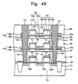
It will be appreciated that the semiconductor device described above, and the methods of fabricating the same, may be applied in various memory devices. For example, the semiconductor device described above may be applied to a DRAM, a non-volatile memory including a gate electrode having a charge trap layer or a floating gate electrode, or a SRAM. When the semiconductor device is an SRAM device, exemplary applications of the semiconductor device described above are described with reference to FIGS. 4A and 4B. Like reference numerals refer to like parts throughout the various figures unless otherwise specified.
Referring to FIG. 3F and 4A, four first transistors 120 may be formed on a semiconductor substrate 10. Two peripherally-arranged first transistors 120 are transfer transistors TT1 and TT2 of the SRAM device. Two centrally-arranged first transistors 120 are drive transistors TD1 and TD2. Source regions 128 s located at both sides of the transfer transistor TT1 and TT2 are connected to bit lines (not shown). The second transistors 150 are load transistors TL1 and TL2 of the SRAM device. Drain regions 146 on the both sides of the load transistors TL1 and TL2 are connected to respective ones of the drain regions 128 d of the transfer transistors TT1 and TT2 by respective ones of first conducting columns 170. The source region 144 between the load transistors TL1 and TL2 is connected to a power line (not shown) by second conducting column 180. The source region 128s located between the drive transistors TD1 and TD2 is grounded.
The number and/or position of first and second conducting columns 170 and 180 shown in FIG. 4A are different from that shown in FIG. 3F. Nevertheless, the first and second conducting columns 170 and 180 shown in FIG. 4A can be formed according to the same methods as described above with respect to FIG. 3F. Moreover, the source/ drain regions 128 s and 128 d can be formed according to the same method as described above with respect to FIG. 3A.
Referring to FIGS. 3F and 4B, third transistors 190 may be formed on the second interlayer insulation layer 160 and a third semiconductor layer 182 may be formed on the third transistors 190 and on the second insulation layer 160. In the illustrated embodiment, the third transistor 190 includes a gate insulation layer 192, a gate electrode 194, a capping pattern 196, and third sidewall spacers 198. An elevated layer 182 a (i.e., a second elevated layer) is additionally formed on source/ drain regions 184 and 186 of the third semiconductor layer 182. The third semiconductor layer 182, the elevated layer 182 a, and the third transistors 190 may be formed in the same manner as the second semiconductor layer 140, the elevated layer 140 a and the second transistors 140 are formed, a detailed description of their formation will be omitted. As shown in FIG. 4B, an epitaxial seed plug 165 may be grown from the elevated layer 140 a of the second semiconductor layer 140 using a SEG method. As similarly described above, the epitaxial seed plug 165 may be as a seed to form the third semiconductor layer 180.
The first transistors 120 may be provided as drive transistors TD1 and TD2, the second transistors 150 may be provided as load transistors TL1 and TL2, and the third transistors 190 may be provided as transfer transistors TT1 and TT2. A third interlayer insulation layer 200 is formed to cover the third transistors 190 on the third semiconductor layer 180. The third interlayer insulation layer 200, the third semiconductor layer 180, the elevated layer 182 a, the second interlayer insulation layer 160, the elevated layer 140 a, the second semiconductor layer 140 and the first interlayer insulation layer 130 may be patterned using a photoresist pattern (not shown) to form contact holes exposing the drain regions 128 d of the first semiconductor layer 110. Additionally, conducting columns 170 may be formed to fill the contact holes. The drain regions 128 d, 146 and 186 of the first semiconductor layer 110, the second semiconductor layer 140 and the third semiconductor layer 180, respectively, may be electrically connected to each other by corresponding ones of the conducting columns 170. Side portions of the conducting columns 170 contact the second semiconductor layer 140, the elevated layer 140 a, the third semiconductor layer 180, and the elevated layer 182 a. As shown in FIG. 4B, the number of first conducting columns 170 is different from that shown in FIG. 3F. Nevertheless, the first conducting columns 170 shown in FIG. 4B can be formed according to the same methods as described above with respect to FIG. 3F. Moreover, the source/ drain regions 128 s and 128 d can be formed according to the same method as described above with respect to FIG. 3A.
According to the embodiments exemplarily described above, an elevated layer that is self-aligned with respect to a sidewall spacer may be formed on source/drain regions without the need for additional patterning or photolithography processes. Accordingly, a leakage current can be reduced by decreasing the thickness of the channel region of the transistors while an electrical contact resistance can be reduced by increasing the contact area between the source/drain regions and a corresponding conducting column.
The above-disclosed subject matter is to be considered illustrative, and not restrictive, and the appended claims are intended to cover all such modifications, enhancements, and other embodiments, which fall within the true spirit and scope of the present invention. Thus, to the maximum extent allowed by law, the scope of the present invention is to be determined by the broadest permissible interpretation of the following claims and their equivalents, and shall not be restricted or limited by the foregoing detailed description.

Claims (13)

1. A semiconductor device, comprising:
a first semiconductor layer;
a first interlayer insulation layer covering the first semiconductor layer;
a second semiconductor layer on the first interlayer insulation layer, the second semiconductor layer comprising a source region, a drain region and a channel region between the source and drain regions;
a gate pattern on the channel region; and
a conducting column extending through at least one of the source and drain regions,
wherein at least one of the source and drain regions comprises a low-concentration impurity region and an elevated high-concentration impurity region, wherein a top surface of the elevated high-concentration impurity region is above a top surface of the channel region, and
wherein at least a portion of a sidewall of each of the low-concentration impurity region and the elevated high-concentration impurity region contacts a side portion of the conducting column.
2. The semiconductor device of claim 1, wherein the top surface of the elevated high-concentration impurity region and at least a portion of a side surface of the elevated high-concentration impurity region are above a top surface of the channel region.
3. The semiconductor device of claim 1, wherein the gate pattern is over the channel region.
4. The semiconductor device of claim 1, wherein the low-concentration impurity region is between the elevated high-concentration impurity region and the first interlayer insulation layer.
5. The semiconductor device of claim 1, wherein the source and drain regions and the elevated high-concentration impurity region comprise an impurity of the same conductivity-type.
6. The semiconductor device of claim 5, wherein the elevated high-concentration impurity region is separated from a bottom portion of the second semiconductor layer.
7. The semiconductor device of claim 1, further comprising a sidewall spacer on a sidewall of the gate pattern, wherein the elevated high-concentration impurity region is self-aligned with respect to the sidewall spacer.
8. The semiconductor device of claim 7, further comprising a capping pattern on the gate pattern.
9. The semiconductor device of claim 8, wherein a crystal structure of the elevated high-concentration impurity region corresponds to a crystal structure of the second semiconductor layer.
10. The semiconductor device of claim 1, the conducting column further comprising a first conducting column extending through the first interlayer insulation layer and the second semiconductor layer, wherein the first conducting column electrically connects the first semiconductor layer and the second semiconductor layer together.
11. The semiconductor device of claim 10, further comprising:
a second interlayer insulation layer covering the second semiconductor layer,
wherein the conducting column comprises a second conducting column extending through the second interlayer insulation layer.
12. The semiconductor device of claim 11, wherein the first and second conducting columns comprise a barrier layer and a conductor material surrounded by the barrier layer.
13. The semiconductor device of claim 11, wherein a bottom portion of the second conducting column contacts the first interlayer insulation layer.
US11/672,875 2006-02-08 2007-02-08 Semiconductor device having stacked transistors Active 2028-02-28 US7741644B2 (en)

Applications Claiming Priority (3)

Application Number Priority Date Filing Date Title
KR1020060012179A KR100714401B1 (en) 2006-02-08 2006-02-08 Semiconductor device having stacked transistors and method of forming the same
KR2006-0012179 2006-02-08
KR10-2006-0012179 2006-02-08

Publications (2)

Publication Number Publication Date
US20070181953A1 US20070181953A1 (en) 2007-08-09
US7741644B2 true US7741644B2 (en) 2010-06-22

Family

ID=38269661

Family Applications (1)

Application Number Title Priority Date Filing Date
US11/672,875 Active 2028-02-28 US7741644B2 (en) 2006-02-08 2007-02-08 Semiconductor device having stacked transistors

Country Status (2)

Country Link
US (1) US7741644B2 (en)
KR (1) KR100714401B1 (en)

Cited By (31)

* Cited by examiner, † Cited by third party
Publication number Priority date Publication date Assignee Title
US20090218628A1 (en) * 2008-02-29 2009-09-03 Hynix Semiconductor Inc. Semiconductor Device and Method for Manufacturing the Same
US20090278167A1 (en) * 2008-05-08 2009-11-12 Desno Corporation Semiconductor device including a plurality of chips and method of manufacturing semiconductor device
US20110089417A1 (en) * 2009-10-21 2011-04-21 Semiconductor Energy Laboratory Co., Ltd. Semiconductor device
US20110089523A1 (en) * 2008-12-10 2011-04-21 Ultratech, Inc. Systems and processes for forming three-dimensional circuits
US20110101334A1 (en) * 2009-10-30 2011-05-05 Semiconductor Energy Laboratory Co., Ltd. Semiconductor device
US20110122670A1 (en) * 2009-11-20 2011-05-26 Semiconductor Energy Laboratory Co., Ltd. Semiconductor device
US20110156117A1 (en) * 2009-12-25 2011-06-30 Semiconductor Energy Laboratory Co., Ltd. Semiconductor device
US20120012837A1 (en) * 2010-07-16 2012-01-19 Semiconductor Energy Laboratory Co., Ltd. Semiconductor device
US8207756B2 (en) 2009-10-30 2012-06-26 Semiconductor Energy Laboratory Co., Ltd. Logic circuit and semiconductor device
US20120181602A1 (en) * 2011-01-13 2012-07-19 Yoshiaki Fukuzumi Semiconductor memory device and method of manufacturing the same
US8415731B2 (en) 2010-01-20 2013-04-09 Semiconductor Energy Laboratory Co., Ltd. Semiconductor storage device with integrated capacitor and having transistor overlapping sections
US8467231B2 (en) 2010-08-06 2013-06-18 Semiconductor Energy Laboratory Co., Ltd. Semiconductor device and driving method thereof
US8471256B2 (en) 2009-11-27 2013-06-25 Semiconductor Energy Laboratory Co., Ltd. Semiconductor device and method for manufacturing the same
US8488394B2 (en) 2010-08-06 2013-07-16 Semiconductor Energy Laboratory Co., Ltd. Semiconductor device
US8680520B2 (en) 2009-11-20 2014-03-25 Semiconductor Energy Laboratory Co., Ltd. Semiconductor device
US8780629B2 (en) 2010-01-15 2014-07-15 Semiconductor Energy Laboratory Co., Ltd. Semiconductor device and driving method thereof
US8896042B2 (en) 2009-10-30 2014-11-25 Semiconductor Energy Laboratory Co., Ltd. Semiconductor device comprising oxide semiconductor
US20150014778A1 (en) * 2013-07-12 2015-01-15 International Business Machines Corporation Multiple via structure and method
US20150187814A1 (en) * 2013-12-26 2015-07-02 Semiconductor Energy Laboratory Co., Ltd. Semiconductor device
US9305630B2 (en) 2013-07-17 2016-04-05 Semiconductor Energy Laboratory Co., Ltd. Semiconductor device and method for driving the same
US9431430B2 (en) * 2012-01-26 2016-08-30 Semiconductor Energy Laboratory Co., Ltd. Semiconductor device and method for manufacturing the same
US9773787B2 (en) 2015-11-03 2017-09-26 Semiconductor Energy Laboratory Co., Ltd. Semiconductor device, memory device, electronic device, or method for driving the semiconductor device
US20170278869A1 (en) * 2016-03-23 2017-09-28 Japan Display Inc. Method for manufacturing semiconductor device
US9780093B2 (en) 2010-07-02 2017-10-03 Semiconductor Energy Laboratory Co., Ltd. Semiconductor device
US10043833B2 (en) 2011-12-01 2018-08-07 Semiconductor Energy Laboratory Co., Ltd. Semiconductor device
US10217736B2 (en) 2013-09-23 2019-02-26 Semiconductor Energy Laboratory Co., Ltd. Semiconductor device including transistor and capacitor
US10236287B2 (en) 2013-09-23 2019-03-19 Semiconductor Energy Laboratory Co., Ltd. Semiconductor device including semiconductor electrically surrounded by electric field of conductive film
US10490553B2 (en) 2009-10-29 2019-11-26 Semiconductor Energy Laboratory Co., Ltd. Semiconductor device
US11114346B2 (en) 2019-08-06 2021-09-07 Tokyo Electron Limited High density logic formation using multi-dimensional laser annealing
US11935929B2 (en) 2021-10-21 2024-03-19 International Business Machines Corporation High aspect ratio shared contacts
US11996408B2 (en) * 2022-04-21 2024-05-28 Intel Corporation Leave-behind protective layer having secondary purpose

Families Citing this family (20)

* Cited by examiner, † Cited by third party
Publication number Priority date Publication date Assignee Title
KR100960451B1 (en) 2008-02-29 2010-05-28 주식회사 하이닉스반도체 Semiconductor device and method for manufacturing the same
KR100955183B1 (en) * 2008-02-29 2010-04-29 주식회사 하이닉스반도체 Semiconductor device and method for manufacturing the same
US7741645B2 (en) * 2008-05-28 2010-06-22 International Business Machines Corporation Three-dimensional integrated heterogeneous semiconductor structure
US8269312B2 (en) * 2008-06-05 2012-09-18 Rohm Co., Ltd. Semiconductor device with resistive element
JP2011119512A (en) * 2009-12-04 2011-06-16 Denso Corp Semiconductor device and method of manufacturing the same
KR101481399B1 (en) 2009-12-18 2015-01-14 가부시키가이샤 한도오따이 에네루기 켄큐쇼 Semiconductor device
US8815660B2 (en) * 2010-02-05 2014-08-26 International Business Machines Corporation Structure and method for reducing floating body effect of SOI MOSFETs
WO2011111507A1 (en) * 2010-03-12 2011-09-15 Semiconductor Energy Laboratory Co., Ltd. Semiconductor device and method for manufacturing the same
US8314001B2 (en) * 2010-04-09 2012-11-20 International Business Machines Corporation Vertical stacking of field effect transistor structures for logic gates
US8546250B2 (en) * 2011-08-18 2013-10-01 Wafertech Llc Method of fabricating vertical integrated semiconductor device with multiple continuous single crystal silicon layers vertically separated from one another
US10002968B2 (en) 2011-12-14 2018-06-19 Semiconductor Energy Laboratory Co., Ltd. Semiconductor device and display device including the same
US9281305B1 (en) * 2014-12-05 2016-03-08 National Applied Research Laboratories Transistor device structure
US9419003B1 (en) * 2015-05-15 2016-08-16 Taiwan Semiconductor Manufacturing Company, Ltd. Semiconductor devices and methods of manufacture thereof
WO2017111802A1 (en) * 2015-12-24 2017-06-29 Intel Corporation Integrated circuit with stacked transistor devices
CN107154407A (en) * 2017-05-17 2017-09-12 厦门天马微电子有限公司 Laminated film transistor device and its manufacture method, display panel and display device
US10340290B2 (en) * 2017-09-15 2019-07-02 Globalfoundries Inc. Stacked SOI semiconductor devices with back bias mechanism
KR102500943B1 (en) 2018-08-24 2023-02-16 삼성전자주식회사 Semiconductor device and method of fabricating thereof
US11616057B2 (en) * 2019-03-27 2023-03-28 Intel Corporation IC including back-end-of-line (BEOL) transistors with crystalline channel material
US11004856B1 (en) * 2019-11-12 2021-05-11 International Business Machines Corporation Stacked vertical transistor memory cell with epi connections
US11744060B2 (en) * 2021-08-12 2023-08-29 Taiwan Semiconductor Manufacturing Company, Ltd. Memory device

Citations (14)

* Cited by examiner, † Cited by third party
Publication number Priority date Publication date Assignee Title
US4272880A (en) * 1979-04-20 1981-06-16 Intel Corporation MOS/SOS Process
US5612552A (en) * 1994-03-31 1997-03-18 Lsi Logic Corporation Multilevel gate array integrated circuit structure with perpendicular access to all active device regions
KR100214558B1 (en) 1997-02-20 1999-08-02 구본준 Stack type inverter and its fabricating process
KR20010106418A (en) 1998-07-23 2001-11-29 추후제출 Method of Etching Doped Silicon Dioxide With Selectivity To Undoped Silicon Dioxide With a High Density Plasma Etcher
US6429484B1 (en) 2000-08-07 2002-08-06 Advanced Micro Devices, Inc. Multiple active layer structure and a method of making such a structure
US6429070B1 (en) * 2000-08-30 2002-08-06 Micron Technology, Inc. DRAM cell constructions, and methods of forming DRAM cells
US20020119640A1 (en) * 2001-02-28 2002-08-29 Fernando Gonzalez Methods of forming semiconductor circuitry, methods of forming logic circuitry, and semiconductor circuit constructions
US6882010B2 (en) 2002-10-03 2005-04-19 Micron Technology, Inc. High performance three-dimensional TFT-based CMOS inverters, and computer systems utilizing such novel CMOS inverters
US20050248035A1 (en) * 2004-04-26 2005-11-10 Yong-Hoon Son Semiconductor devices having contact plugs with stress buffer spacers and methods of fabricating the same
US20060102959A1 (en) * 2004-11-16 2006-05-18 Samsung Electronics Co., Ltd. Semiconductor integrated circuit devices having single crystalline thin film transistors and methods of fabricating the same
US20060115944A1 (en) * 2004-11-26 2006-06-01 Kun-Ho Kwak Methods of fabricating a semiconductor device having a node contact structure of a CMOS inverter
US20060237725A1 (en) * 2005-04-20 2006-10-26 Samsung Electronics Co., Ltd. Semiconductor devices having thin film transistors and methods of fabricating the same
US20070181957A1 (en) * 2006-02-03 2007-08-09 Samsung Electronics Co., Ltd. Semiconductor device having stacked transistors and method for manufacturing the same
US20070215906A1 (en) * 2006-03-15 2007-09-20 Marvell International Ltd. Method for fabricating 1t-dram on bulk silicon

Family Cites Families (2)

* Cited by examiner, † Cited by third party
Publication number Priority date Publication date Assignee Title
KR100649821B1 (en) * 2000-12-26 2006-11-24 주식회사 하이닉스반도체 Manufacturing method for transistor of semiconductor device
KR100746220B1 (en) * 2004-01-12 2007-08-03 삼성전자주식회사 Semiconductor integrated circuits employing stacked node contact structures and stacked thin film transistors and methods of fabricating the same

Patent Citations (14)

* Cited by examiner, † Cited by third party
Publication number Priority date Publication date Assignee Title
US4272880A (en) * 1979-04-20 1981-06-16 Intel Corporation MOS/SOS Process
US5612552A (en) * 1994-03-31 1997-03-18 Lsi Logic Corporation Multilevel gate array integrated circuit structure with perpendicular access to all active device regions
KR100214558B1 (en) 1997-02-20 1999-08-02 구본준 Stack type inverter and its fabricating process
KR20010106418A (en) 1998-07-23 2001-11-29 추후제출 Method of Etching Doped Silicon Dioxide With Selectivity To Undoped Silicon Dioxide With a High Density Plasma Etcher
US6429484B1 (en) 2000-08-07 2002-08-06 Advanced Micro Devices, Inc. Multiple active layer structure and a method of making such a structure
US6429070B1 (en) * 2000-08-30 2002-08-06 Micron Technology, Inc. DRAM cell constructions, and methods of forming DRAM cells
US20020119640A1 (en) * 2001-02-28 2002-08-29 Fernando Gonzalez Methods of forming semiconductor circuitry, methods of forming logic circuitry, and semiconductor circuit constructions
US6882010B2 (en) 2002-10-03 2005-04-19 Micron Technology, Inc. High performance three-dimensional TFT-based CMOS inverters, and computer systems utilizing such novel CMOS inverters
US20050248035A1 (en) * 2004-04-26 2005-11-10 Yong-Hoon Son Semiconductor devices having contact plugs with stress buffer spacers and methods of fabricating the same
US20060102959A1 (en) * 2004-11-16 2006-05-18 Samsung Electronics Co., Ltd. Semiconductor integrated circuit devices having single crystalline thin film transistors and methods of fabricating the same
US20060115944A1 (en) * 2004-11-26 2006-06-01 Kun-Ho Kwak Methods of fabricating a semiconductor device having a node contact structure of a CMOS inverter
US20060237725A1 (en) * 2005-04-20 2006-10-26 Samsung Electronics Co., Ltd. Semiconductor devices having thin film transistors and methods of fabricating the same
US20070181957A1 (en) * 2006-02-03 2007-08-09 Samsung Electronics Co., Ltd. Semiconductor device having stacked transistors and method for manufacturing the same
US20070215906A1 (en) * 2006-03-15 2007-09-20 Marvell International Ltd. Method for fabricating 1t-dram on bulk silicon

Non-Patent Citations (1)

* Cited by examiner, † Cited by third party
Title
English language abstract of Korean Publication No. 10-0214558.

Cited By (65)

* Cited by examiner, † Cited by third party
Publication number Priority date Publication date Assignee Title
US20090218628A1 (en) * 2008-02-29 2009-09-03 Hynix Semiconductor Inc. Semiconductor Device and Method for Manufacturing the Same
US8324070B2 (en) * 2008-02-29 2012-12-04 Hynix Semiconductor Inc. Semiconductor device and method for manufacturing the same
US8018008B2 (en) * 2008-05-08 2011-09-13 Denso Corporation Semiconductor device including a plurality of chips and method of manufacturing semiconductor device
US20090278167A1 (en) * 2008-05-08 2009-11-12 Desno Corporation Semiconductor device including a plurality of chips and method of manufacturing semiconductor device
US20110089523A1 (en) * 2008-12-10 2011-04-21 Ultratech, Inc. Systems and processes for forming three-dimensional circuits
US20110089417A1 (en) * 2009-10-21 2011-04-21 Semiconductor Energy Laboratory Co., Ltd. Semiconductor device
US10490553B2 (en) 2009-10-29 2019-11-26 Semiconductor Energy Laboratory Co., Ltd. Semiconductor device
US9722086B2 (en) 2009-10-30 2017-08-01 Semiconductor Energy Laboratory Co., Ltd. Logic circuit and semiconductor device
US9685447B2 (en) 2009-10-30 2017-06-20 Semiconductor Energy Laboratory Co., Ltd. Semiconductor device comprising transistor including oxide semiconductor
US8207756B2 (en) 2009-10-30 2012-06-26 Semiconductor Energy Laboratory Co., Ltd. Logic circuit and semiconductor device
US11963374B2 (en) 2009-10-30 2024-04-16 Semiconductor Energy Laboratory Co., Ltd. Semiconductor device
US8570070B2 (en) 2009-10-30 2013-10-29 Semiconductor Energy Laboratory Co., Ltd. Logic circuit and semiconductor device
US9373640B2 (en) 2009-10-30 2016-06-21 Semiconductor Energy Laboratory Co., Ltd. Semiconductor device
US10510757B2 (en) 2009-10-30 2019-12-17 Semiconductor Energy Laboratory Co., Ltd. Semiconductor device including storage element
US9105511B2 (en) 2009-10-30 2015-08-11 Semiconductor Energy Laboratory Co., Ltd. Semiconductor device comprising oxide semiconductor
US20110101334A1 (en) * 2009-10-30 2011-05-05 Semiconductor Energy Laboratory Co., Ltd. Semiconductor device
US10811417B2 (en) 2009-10-30 2020-10-20 Semiconductor Energy Laboratory Co., Ltd. Semiconductor device
US8896042B2 (en) 2009-10-30 2014-11-25 Semiconductor Energy Laboratory Co., Ltd. Semiconductor device comprising oxide semiconductor
US8860108B2 (en) 2009-10-30 2014-10-14 Semiconductor Energy Laboratory Co., Ltd. Oxide-based thin-film transistor (TFT) semiconductor memory device having source/drain electrode of one transistor connected to gate electrode of the other
US11322498B2 (en) 2009-10-30 2022-05-03 Semiconductor Energy Laboratory Co., Ltd. Semiconductor device
US8680520B2 (en) 2009-11-20 2014-03-25 Semiconductor Energy Laboratory Co., Ltd. Semiconductor device
US8619454B2 (en) 2009-11-20 2013-12-31 Semiconductor Energy Laboratory Co., Ltd. Semiconductor device
US8339828B2 (en) 2009-11-20 2012-12-25 Semiconductor Energy Laboratory Co., Ltd. Semiconductor device
US9135958B2 (en) 2009-11-20 2015-09-15 Semiconductor Energy Laboratory Co., Ltd. Semiconductor device
US8804396B2 (en) 2009-11-20 2014-08-12 Semiconductor Energy Laboratory Co., Ltd. Semiconductor device
US9705005B2 (en) 2009-11-20 2017-07-11 Semiconductor Energy Laboratory Co., Ltd. Semiconductor device
US20110122670A1 (en) * 2009-11-20 2011-05-26 Semiconductor Energy Laboratory Co., Ltd. Semiconductor device
US11894486B2 (en) 2009-11-27 2024-02-06 Semiconductor Energy Laboratory Co., Ltd. Method for manufacturing semiconductor device
US9748436B2 (en) 2009-11-27 2017-08-29 Semiconductor Energy Laboratory Co., Ltd. Semiconductor device and method for manufacturing the same
US8471256B2 (en) 2009-11-27 2013-06-25 Semiconductor Energy Laboratory Co., Ltd. Semiconductor device and method for manufacturing the same
US10396236B2 (en) 2009-11-27 2019-08-27 Semiconductor Energy Laboratory Co., Ltd. Semiconductor device and display device
US20190109259A1 (en) 2009-11-27 2019-04-11 Semiconductor Energy Laboratory Co., Ltd. Semiconductor device and method for manufacturing the same
US8482001B2 (en) 2009-12-25 2013-07-09 Semiconductor Energy Laboratory Co., Ltd. Semiconductor device
US9054201B2 (en) 2009-12-25 2015-06-09 Semiconductor Energy Laboratory Co., Ltd. Semiconductor device
US11676975B2 (en) 2009-12-25 2023-06-13 Semiconductor Energy Laboratory Co., Ltd. Semiconductor device
US20110156117A1 (en) * 2009-12-25 2011-06-30 Semiconductor Energy Laboratory Co., Ltd. Semiconductor device
US10083996B2 (en) 2009-12-25 2018-09-25 Semiconductor Energy Laboratory Co., Ltd. Semiconductor device
US9136280B2 (en) 2010-01-15 2015-09-15 Semiconductor Energy Laboratory Co., Ltd. Semiconductor device and driving method thereof
US8780629B2 (en) 2010-01-15 2014-07-15 Semiconductor Energy Laboratory Co., Ltd. Semiconductor device and driving method thereof
US8415731B2 (en) 2010-01-20 2013-04-09 Semiconductor Energy Laboratory Co., Ltd. Semiconductor storage device with integrated capacitor and having transistor overlapping sections
US10319723B2 (en) 2010-07-02 2019-06-11 Semiconductor Energy Laboratory Co., Ltd. Semiconductor device
US11233055B2 (en) 2010-07-02 2022-01-25 Semiconductor Energy Laboratory Co., Ltd. Semiconductor device
US9780093B2 (en) 2010-07-02 2017-10-03 Semiconductor Energy Laboratory Co., Ltd. Semiconductor device
US20120012837A1 (en) * 2010-07-16 2012-01-19 Semiconductor Energy Laboratory Co., Ltd. Semiconductor device
US8461586B2 (en) * 2010-07-16 2013-06-11 Semiconductor Energy Laboratory Co., Ltd. Semiconductor device
US8847326B2 (en) 2010-07-16 2014-09-30 Semiconductor Energy Laboratory Co., Ltd. Semiconductor device
US8467231B2 (en) 2010-08-06 2013-06-18 Semiconductor Energy Laboratory Co., Ltd. Semiconductor device and driving method thereof
US8488394B2 (en) 2010-08-06 2013-07-16 Semiconductor Energy Laboratory Co., Ltd. Semiconductor device
US8837232B2 (en) 2010-08-06 2014-09-16 Semiconductor Energy Laboratory Co., Ltd. Semiconductor device
US20120181602A1 (en) * 2011-01-13 2012-07-19 Yoshiaki Fukuzumi Semiconductor memory device and method of manufacturing the same
US8476708B2 (en) * 2011-01-13 2013-07-02 Kabushiki Kaisha Toshiba Semiconductor memory device having a circuit formed on a single crystal semiconductor layer with varied germanium concentration
US10043833B2 (en) 2011-12-01 2018-08-07 Semiconductor Energy Laboratory Co., Ltd. Semiconductor device
US9431430B2 (en) * 2012-01-26 2016-08-30 Semiconductor Energy Laboratory Co., Ltd. Semiconductor device and method for manufacturing the same
US9508640B2 (en) * 2013-07-12 2016-11-29 GlobalFoundries, Inc. Multiple via structure and method
US20150014778A1 (en) * 2013-07-12 2015-01-15 International Business Machines Corporation Multiple via structure and method
US9305630B2 (en) 2013-07-17 2016-04-05 Semiconductor Energy Laboratory Co., Ltd. Semiconductor device and method for driving the same
US10236287B2 (en) 2013-09-23 2019-03-19 Semiconductor Energy Laboratory Co., Ltd. Semiconductor device including semiconductor electrically surrounded by electric field of conductive film
US10217736B2 (en) 2013-09-23 2019-02-26 Semiconductor Energy Laboratory Co., Ltd. Semiconductor device including transistor and capacitor
US20150187814A1 (en) * 2013-12-26 2015-07-02 Semiconductor Energy Laboratory Co., Ltd. Semiconductor device
US9466615B2 (en) * 2013-12-26 2016-10-11 Semiconductor Energy Laboratory Co., Ltd. Semiconductor device
US9773787B2 (en) 2015-11-03 2017-09-26 Semiconductor Energy Laboratory Co., Ltd. Semiconductor device, memory device, electronic device, or method for driving the semiconductor device
US20170278869A1 (en) * 2016-03-23 2017-09-28 Japan Display Inc. Method for manufacturing semiconductor device
US11114346B2 (en) 2019-08-06 2021-09-07 Tokyo Electron Limited High density logic formation using multi-dimensional laser annealing
US11935929B2 (en) 2021-10-21 2024-03-19 International Business Machines Corporation High aspect ratio shared contacts
US11996408B2 (en) * 2022-04-21 2024-05-28 Intel Corporation Leave-behind protective layer having secondary purpose

Also Published As

Publication number Publication date
KR100714401B1 (en) 2007-05-04
US20070181953A1 (en) 2007-08-09

Similar Documents

Publication Publication Date Title
US7741644B2 (en) Semiconductor device having stacked transistors
US9202921B2 (en) Semiconductor device and method of making the same
US20090008714A1 (en) Semiconductor devices and methods of forming the same
KR20220129607A (en) Method for forming a three-dimensional memory device having a back surface source contact
US11894371B2 (en) Integrated circuit devices
WO2006011632A2 (en) Semiconductor device including a conductive layer buried in an opening and method of manufacturing the same
CN112086455B (en) Semiconductor device and method for manufacturing the same
US20070257324A1 (en) Semiconductor Devices Having Gate Structures and Contact Pads that are Lower than the Gate Structures
US20080111194A1 (en) Semiconductor device including a finfet
CN110797306A (en) Semiconductor device and method for manufacturing the same
US8928073B2 (en) Semiconductor devices including guard ring structures
CN111276490A (en) Three-dimensional memory and manufacturing method thereof
US20210320008A1 (en) Method for fabricating semiconductor device
US20110101467A1 (en) Stacked semiconductor device and method of manufacturing the same
US8994084B2 (en) Dynamic random access memory and method for fabricating the same
CN113690173A (en) Three-dimensional memory and preparation method thereof
US20230378001A1 (en) Semiconductor device and method
US20230380144A1 (en) Semiconductor device and method for fabricating the same
US20220319567A1 (en) Fft-dram
US20080173924A1 (en) Semiconductor device and method for manufacturing semiconductor device
CN115621195A (en) Semiconductor device and method for manufacturing the same
US7566947B2 (en) Semiconductor device with bipolar transistor and method of fabricating the same
US20090020816A1 (en) Semiconductor device and method of forming the same
US20060017118A1 (en) Semiconductor device having spacer pattern and method of forming the same
US20090078998A1 (en) Semiconductor device having decreased contact resistance

Legal Events

Date Code Title Description
AS Assignment

Owner name: SAMSUNG ELECTRONICS CO., LTD.,KOREA, REPUBLIC OF

Free format text: ASSIGNMENT OF ASSIGNORS INTEREST;ASSIGNORS:LYU, GYU-HO;KIM, SEUG-GYU;REEL/FRAME:018871/0288

Effective date: 20070102

Owner name: SAMSUNG ELECTRONICS CO., LTD., KOREA, REPUBLIC OF

Free format text: ASSIGNMENT OF ASSIGNORS INTEREST;ASSIGNORS:LYU, GYU-HO;KIM, SEUG-GYU;REEL/FRAME:018871/0288

Effective date: 20070102

STCF Information on status: patent grant

Free format text: PATENTED CASE

FPAY Fee payment

Year of fee payment: 4

MAFP Maintenance fee payment

Free format text: PAYMENT OF MAINTENANCE FEE, 8TH YEAR, LARGE ENTITY (ORIGINAL EVENT CODE: M1552)

Year of fee payment: 8

MAFP Maintenance fee payment

Free format text: PAYMENT OF MAINTENANCE FEE, 12TH YEAR, LARGE ENTITY (ORIGINAL EVENT CODE: M1553); ENTITY STATUS OF PATENT OWNER: LARGE ENTITY

Year of fee payment: 12