US7736176B2 - Modular jack assembly having improved connecting terminal - Google Patents
Modular jack assembly having improved connecting terminal Download PDFInfo
- Publication number
- US7736176B2 US7736176B2 US12/074,360 US7436008A US7736176B2 US 7736176 B2 US7736176 B2 US 7736176B2 US 7436008 A US7436008 A US 7436008A US 7736176 B2 US7736176 B2 US 7736176B2
- Authority
- US
- United States
- Prior art keywords
- modular jack
- base element
- terminal
- assembly
- jack assembly
- Prior art date
- Legal status (The legal status is an assumption and is not a legal conclusion. Google has not performed a legal analysis and makes no representation as to the accuracy of the status listed.)
- Expired - Fee Related, expires
Links
Images


Classifications
-
- H—ELECTRICITY
- H01—ELECTRIC ELEMENTS
- H01R—ELECTRICALLY-CONDUCTIVE CONNECTIONS; STRUCTURAL ASSOCIATIONS OF A PLURALITY OF MUTUALLY-INSULATED ELECTRICAL CONNECTING ELEMENTS; COUPLING DEVICES; CURRENT COLLECTORS
- H01R13/00—Details of coupling devices of the kinds covered by groups H01R12/70 or H01R24/00 - H01R33/00
- H01R13/66—Structural association with built-in electrical component
- H01R13/665—Structural association with built-in electrical component with built-in electronic circuit
- H01R13/6658—Structural association with built-in electrical component with built-in electronic circuit on printed circuit board
-
- H—ELECTRICITY
- H01—ELECTRIC ELEMENTS
- H01R—ELECTRICALLY-CONDUCTIVE CONNECTIONS; STRUCTURAL ASSOCIATIONS OF A PLURALITY OF MUTUALLY-INSULATED ELECTRICAL CONNECTING ELEMENTS; COUPLING DEVICES; CURRENT COLLECTORS
- H01R24/00—Two-part coupling devices, or either of their cooperating parts, characterised by their overall structure
- H01R24/60—Contacts spaced along planar side wall transverse to longitudinal axis of engagement
- H01R24/62—Sliding engagements with one side only, e.g. modular jack coupling devices
- H01R24/64—Sliding engagements with one side only, e.g. modular jack coupling devices for high frequency, e.g. RJ 45
Definitions
- the present invention relates to a modular jack assembly and particularly to a modular jack assembly comprising an improved connecting terminal.
- Modular jack assembly is commonly used in the computer or network appliance as input/output port for transmitting data or signals.
- An example of such a connector is disclosed in U.S. Pat. No. 7,052,315 issued on May 30, 2006.
- the modular jack assembly engages with a mating plug and includes an insulative housing, a terminal module received in the housing, a main board mounted to the rear of the insulative housing and a power over ethernet assembly.
- the terminal module includes a base element defining a receiving room and a conductive portion assembled to a front wall of the base element.
- the base element comprises a printed circuit board positioned on a top thereof.
- the terminal module has a plurality of L-shaped signal contacts and power contacts. The L-shaped contacts have first ends routed through the printed circuit board and second ends extending outwardly from a rear wall of the connecting portion and then through the main board for electrically connecting with the power over ethernet assembly.
- the first ends and the second ends of the L-shaped contacts are respectively inserted through the printed circuit board and the main board by strong mechanical force that would result in cracks of the contacts and would complicate the manufacture of the modular jack assembly.
- One object of the present invention is to provide a modular jack assembly comprising a terminal module having an improved connecting terminal adapted for being assembled to the terminal module easily and being fixed in corresponding terminal slots firmly.
- the present invention provides a modular jack assembly for being mounted on a mother board and engaging with a mating plug.
- the modular jack assembly comprises a plurality of terminal modules, an outer shield surrounding the insulative housing, a power over ethernet assembly mounted rearwardly.
- the terminal module comprises a contacting module, a base element, a connecting element, a pair of daughter boards assembled to opposite sides of the base element and a plurality of connecting terminals mounted to the base element.
- the base element defines a plurality of terminal slots at an outer face thereof for receiving the connecting terminals.
- Each connecting terminal has a first end exposed at a side of the base element, a second end connected with the power over ethernet assembly and a plurality of protrusions disposed thereon for interfering with the terminal slots.
- the connecting terminals are easy to be mounted into the terminal slot in an outer-to-inner direction and firmly fixed in the terminal slots by the interference between the protrusions of the connecting terminals and the terminal slots.
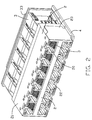
- FIG. 1 is an assembled view of the modular jack assembly mounted on a mother board
- FIG. 2 is a partially assembled view of the modular jack assembly mounted on the mother board, with an outer shield being removed;
- FIG. 3 is an assembled perspective view of a terminal module which is connected with a power over ethernet assembly
- FIG. 4 is an assembled perspective view of the terminal module which is connected with the power over ethernet assembly and the mother board;
- FIG. 5 is an exploded view of the terminal module as shown in FIG. 3 ;
- FIG. 6 is an exploded view of a base element of the terminal module as shown in FIG. 5 ;
- FIG. 7 is another perspective view of the base element as shown in FIG. 6 .
- a modular jack assembly 1 for being mounted on a mother board 4 and engaging with a mating plug comprises an insulative housing 2 , a plurality of terminal modules 3 mounted in the insulative housing 2 , a power over ethernet assembly 33 rearwardly assembled to the terminal module 3 and an outer shield 6 surrounding the insulative housing 2 .
- the insulative housing 2 has a pair of lateral walls 23 , a top wall 21 , and a bottom wall 22 and defines a plurality of cavities 20 for receiving the mating plugs.
- the power over ethernet assembly 33 is provided with a substrate 5 and a plurality of electrical elements 330 mounted to the substrate 5 .
- the terminal module 3 is mounted in the cavity 20 of the insulative housing 2 and comprises a contacting module 30 , a base element 310 , a pair of daughter boards 311 having a plurality of magnetic cores 312 mounted thereon, and a connecting element 32 .
- the terminal module 3 further has a plurality of connecting terminals 35 mounted to the base element 310 .
- the connecting element 32 is mounted to a bottom portion of base element 310 for connecting with the mother board 4 .
- the contacting module 30 is mounted to the base element 310 .
- the contacting module 30 has a rectangular housing 301 and two groups of mating terminals 302 in the rectangular housing 301 .
- the mating terminals 302 have a plurality of contacting portions 3022 received in the cavities 20 of the insulative housing 2 for electrically connecting with the mating plug, and a plurality of tail portions 3021 extending perpendicularly from the rectangular housing 301 into a plurality of second holes 3110 disposed on the daughter board 311 , thereby forming a conductive trace between the daughter board 311 and the contacting module 30 .
- the base element 310 has a front portion 3101 , a top portion 3103 , a bottom portion 3104 , a rear portion 3102 , a pair of opposite side faces 3107 and a pair of receiving rooms 3108 defined therebetween for receiving the magnetic cores 312 of the daughter boards 311 .
- the front portion 3101 defines an opening 3105 for engaging with the rectangular housing 301 of the contacting module 30 .
- the base element 310 further comprises a first projecting portion 313 rearwardly of the top portion 3103 and a second projecting portion 314 extending from the bottom portion 3104 .
- a receiving space 315 is formed between the first projecting portion 313 and the second projecting portion 314 and is adapted for receiving the electrical elements 330 of the power over ethernet assembly 33 .
- the first projecting portion 313 comprises a middle section 3130 horizontally rearwardly extending from the top portion 3103 of the base element 310 and a pair of opposite lateral walls 3131 perpendicularly downwardly extending from the middle section 3130 .
- Each lateral wall 3131 has a pair of parallel terminal slots 3132 thereon for receiving the connecting terminals 35 .
- the bottom portion 3104 of the base element 310 is provided with a pair of posts 3106 extending downwardly.
- the connecting terminal 35 comprises a lengthwise section 354 , a first end 351 extending perpendicularly from the lengthwise section 354 and exposed at a side of the first projecting portion 313 , a second end 352 extending rearwardly from the lengthwise section 354 for electrically connecting with the power over ethernet assembly 33 , and a plurality of protrusions 353 projecting perpendicularly from the lengthwise section 354 for interfering with the terminal slots 3132 .
- the first end 351 extends into a first hole 3111 disposed on daughter board 311 .
- the second end 352 extends perpendicularly outwardly from the terminal slot 3132 , for electrically connecting with the power over ethernet assembly 33 .
- An electrical connection between the daughter board 311 and the power over ethernet assembly 33 is established.
- the connecting element 32 is mounted below the bottom portion 3104 of the base element 310 .
- the connecting element 32 has a base section 321 defining a pair of recesses 322 thereon for engaging with a pair of protruding posts 3106 of the base element 310 , and two rows of L-shaped contacts 323 assembled to the base section 321 .
- Each row of the L-shaped contacts 323 have soldering portions 324 soldered onto the mother board 4 and bending portions 325 extending through a plurality of third holes 3112 disposed on the daughter board 311 , thereby forming a conductive trace between the daughter board 311 and the mother board 4 .
- the third holes 3112 are defined along a lower edge of the daughter board 311 and are positioned away from the second holes 3110 for avoiding hi-pot.
- the modular jack assembly further comprises a grounding plate 34 defining a plurality of through holes (not shown) for extension of the L-shaped contacts 323 .
- the connecting terminals 35 are inserted into the terminal slots 3132 in an outer-to-inner manner along a direction perpendicular to the extending direction of the lateral wall 3131 .
- the protrusions 353 of the connecting terminals 35 interfere with the terminal slots 3132 for firmly fixing the connecting terminals 35 .
- the contacting module 30 is inserted into the opening 3105 of the base element 310 .
- the connecting element 32 is mounted below the bottom portion 3104 of the base element 310 by the engagement between the protruding posts 3106 and the recesses 322 .
- the pair of daughter boards 31 are assembled to the side faces 3107 of the base element 310 and the magnetic cores 312 of the daughter board 31 are received in the receiving room 3108 .
- the power over ethernet assembly 33 is mounted to the rear portion of the base element 310 and is electrically connected with the connecting terminals 35 .
- the terminal module 3 is assembled as a whole.
- the grounding plate 34 is mounted below the terminal module 3 .
- the soldering portions 324 of the L-shaped contacts 323 extend through corresponding through holes of the grounding plate 34 for being fixed at a proper position.
- the terminal module 3 is mounted in the cavity 20 of the insulative housing 2 and then the assembly is ready to be mounted to the mother board 4 .
- the soldering portions 324 of the L-shaped contacts 323 are soldered on the mother board 4 .
- the outer shield 6 is attached to an outer side of the insulative housing 2 for shielding purpose.
- the grounding plate 34 is connected to the outer shield 6 for grounding.
- the terminal module 3 is electrically connected to the mother board 4 via the electrical connection among the mating terminals 302 , a conductive trace of the daughter board 311 and the L-shaped contacts 323 .
- the terminal module 3 is electrically connected to the electrical elements 330 of the power over ethernet assembly 33 via the electrical connection among the mating terminals 302 , another conductive trace of the daughter board 311 and the connecting terminals 35 .
Landscapes
- Engineering & Computer Science (AREA)
- Microelectronics & Electronic Packaging (AREA)
- Details Of Connecting Devices For Male And Female Coupling (AREA)
- Coupling Device And Connection With Printed Circuit (AREA)
Abstract
Description
Claims (16)
Applications Claiming Priority (3)
| Application Number | Priority Date | Filing Date | Title |
|---|---|---|---|
| CN200720034865.5 | 2007-03-02 | ||
| CNU2007200348655U CN201029178Y (en) | 2007-03-02 | 2007-03-02 | Electric connecting assembly |
| CN200720034865 | 2007-03-02 |
Publications (2)
| Publication Number | Publication Date |
|---|---|
| US20080214057A1 US20080214057A1 (en) | 2008-09-04 |
| US7736176B2 true US7736176B2 (en) | 2010-06-15 |
Family
ID=39133390
Family Applications (1)
| Application Number | Title | Priority Date | Filing Date |
|---|---|---|---|
| US12/074,360 Expired - Fee Related US7736176B2 (en) | 2007-03-02 | 2008-03-03 | Modular jack assembly having improved connecting terminal |
Country Status (2)
| Country | Link |
|---|---|
| US (1) | US7736176B2 (en) |
| CN (1) | CN201029178Y (en) |
Cited By (10)
| Publication number | Priority date | Publication date | Assignee | Title |
|---|---|---|---|---|
| US20120052718A1 (en) * | 2010-08-26 | 2012-03-01 | Pocrass Alan L | High Frequency Local and Wide Area Networking Connector with Insertable and Removable Tranformer Component and Heat Sink |
| US20120115364A1 (en) * | 2010-11-05 | 2012-05-10 | Hon Hai Precision Industry Co., Ltd. | Electrical connector having improved grounding members |
| US20120142199A1 (en) * | 2010-12-02 | 2012-06-07 | Molex Incorporated | Filtering assembly and modular jack using same |
| US8235731B1 (en) * | 2011-03-18 | 2012-08-07 | Leviton Manufacturing Co., Ltd. | Connector module and patch panel |
| US20140154895A1 (en) * | 2012-07-05 | 2014-06-05 | Leviton Manufacturing Co., Inc. | High density high speed data communications connector |
| US20140206226A1 (en) * | 2011-01-28 | 2014-07-24 | Hon Hai Precision Industry Co., Ltd. | Electrical connector having shielding member |
| US20150147914A1 (en) * | 2013-11-22 | 2015-05-28 | Foxconn Interconnect Technology Limited | Electrical connector having an improved structure for assembling a contact module to an insulative housing |
| US9397450B1 (en) * | 2015-06-12 | 2016-07-19 | Amphenol Corporation | Electrical connector with port light indicator |
| US9419391B2 (en) | 2013-08-20 | 2016-08-16 | Panduit Corp. | Communication connector |
| US11811163B2 (en) | 2021-02-26 | 2023-11-07 | Leviton Manufacturing Co., Inc. | Mutoa and quad floating connector |
Families Citing this family (1)
| Publication number | Priority date | Publication date | Assignee | Title |
|---|---|---|---|---|
| CN101262107B (en) * | 2007-03-05 | 2011-06-29 | 富士康(昆山)电脑接插件有限公司 | Electric connector component |
Citations (2)
| Publication number | Priority date | Publication date | Assignee | Title |
|---|---|---|---|---|
| US7052315B2 (en) | 2004-06-16 | 2006-05-30 | Tyco Electronics Corporation | Stacked jack assembly providing multiple configurations |
| US7517254B2 (en) * | 2007-03-05 | 2009-04-14 | Hon Hai Precision Ind. Co., Ltd. | Modular jack assembly having improved base element |
-
2007
- 2007-03-02 CN CNU2007200348655U patent/CN201029178Y/en not_active Expired - Fee Related
-
2008
- 2008-03-03 US US12/074,360 patent/US7736176B2/en not_active Expired - Fee Related
Patent Citations (2)
| Publication number | Priority date | Publication date | Assignee | Title |
|---|---|---|---|---|
| US7052315B2 (en) | 2004-06-16 | 2006-05-30 | Tyco Electronics Corporation | Stacked jack assembly providing multiple configurations |
| US7517254B2 (en) * | 2007-03-05 | 2009-04-14 | Hon Hai Precision Ind. Co., Ltd. | Modular jack assembly having improved base element |
Cited By (17)
| Publication number | Priority date | Publication date | Assignee | Title |
|---|---|---|---|---|
| US20120052718A1 (en) * | 2010-08-26 | 2012-03-01 | Pocrass Alan L | High Frequency Local and Wide Area Networking Connector with Insertable and Removable Tranformer Component and Heat Sink |
| US8357010B2 (en) * | 2010-08-26 | 2013-01-22 | Pocrass Alan L | High frequency local and wide area networking connector with insertable and removable tranformer component and heat sink |
| US20120115364A1 (en) * | 2010-11-05 | 2012-05-10 | Hon Hai Precision Industry Co., Ltd. | Electrical connector having improved grounding members |
| US8403701B2 (en) * | 2010-11-05 | 2013-03-26 | Hon Hai Precision Ind. Co., Ltd | Electrical connector having improved grounding members |
| US8545274B2 (en) | 2010-12-02 | 2013-10-01 | Molex Incorporated | Filtering assembly and modular jack using same |
| US20120142199A1 (en) * | 2010-12-02 | 2012-06-07 | Molex Incorporated | Filtering assembly and modular jack using same |
| US8449332B2 (en) * | 2010-12-02 | 2013-05-28 | Molex Incorporated | Filtering assembly and modular jack using same |
| US9252530B2 (en) * | 2011-01-28 | 2016-02-02 | Hon Hai Precision Industry Co., Ltd. | Electrical connector having shielding member |
| US20140206226A1 (en) * | 2011-01-28 | 2014-07-24 | Hon Hai Precision Industry Co., Ltd. | Electrical connector having shielding member |
| US8235731B1 (en) * | 2011-03-18 | 2012-08-07 | Leviton Manufacturing Co., Ltd. | Connector module and patch panel |
| US20140154895A1 (en) * | 2012-07-05 | 2014-06-05 | Leviton Manufacturing Co., Inc. | High density high speed data communications connector |
| US9147977B2 (en) * | 2012-07-05 | 2015-09-29 | Leviton Manufacturing Co., Inc. | High density high speed data communications connector |
| US9419391B2 (en) | 2013-08-20 | 2016-08-16 | Panduit Corp. | Communication connector |
| US20150147914A1 (en) * | 2013-11-22 | 2015-05-28 | Foxconn Interconnect Technology Limited | Electrical connector having an improved structure for assembling a contact module to an insulative housing |
| US9531109B2 (en) * | 2013-11-22 | 2016-12-27 | Foxconn Interconnect Technology Limited | Electrical connector having an improved structure for assembling a contact module to an insulative housing |
| US9397450B1 (en) * | 2015-06-12 | 2016-07-19 | Amphenol Corporation | Electrical connector with port light indicator |
| US11811163B2 (en) | 2021-02-26 | 2023-11-07 | Leviton Manufacturing Co., Inc. | Mutoa and quad floating connector |
Also Published As
| Publication number | Publication date |
|---|---|
| US20080214057A1 (en) | 2008-09-04 |
| CN201029178Y (en) | 2008-02-27 |
Similar Documents
| Publication | Publication Date | Title |
|---|---|---|
| US7517254B2 (en) | Modular jack assembly having improved base element | |
| US7736176B2 (en) | Modular jack assembly having improved connecting terminal | |
| US7153158B1 (en) | Stacked module connector | |
| US6875031B1 (en) | Electrical connector with circuit board module | |
| US8152568B2 (en) | Cable assembly with new interface | |
| US7775829B2 (en) | Electrical connector | |
| US6641438B1 (en) | High speed, high density backplane connector | |
| US7390219B2 (en) | Electrical connector having improved outer shield | |
| US7775828B2 (en) | Electrical connector having improved grounding member | |
| US7485004B2 (en) | Electrical connector having improved electrical element | |
| US20120045920A1 (en) | Cable assembly with a new interface | |
| US7648390B2 (en) | Electrical connector having individual shell | |
| US8215982B2 (en) | Electrical connector having reliable connection between LED devices and printed circuit board | |
| US20110111628A1 (en) | Cable assembly and method of manufacturing the same | |
| US8579660B2 (en) | High speed modular jack | |
| US20080020654A1 (en) | Upright electrical connector | |
| US9431769B2 (en) | Electrical connector having improved shielding | |
| EP1190469A1 (en) | Modular electrical connector and connector system | |
| US9246276B2 (en) | Electrical connector having a shielding member disposed between two magnetic modules | |
| US6918791B2 (en) | Electrical connector having a reliable internal circuit board | |
| US6659807B1 (en) | Electrical connector with insert-molding structure | |
| US6739915B1 (en) | Electrical connector with rear retention mechanism of outer shell | |
| US20120208405A1 (en) | Plug connector having an arrangement of terminals and a connector assembly having the same | |
| US7261592B2 (en) | Electrical connector | |
| US20080248695A1 (en) | Modular jack with improved grounding member |
Legal Events
| Date | Code | Title | Description |
|---|---|---|---|
| AS | Assignment |
Owner name: HON HAI PRECISION IND. CO., LTD., TAIWAN Free format text: ASSIGNMENT OF ASSIGNORS INTEREST;ASSIGNORS:ZHANG, HONG-BO;XU, ZHENG-HUA;WU, LI-CHUN;REEL/FRAME:020650/0081 Effective date: 20080218 Owner name: HON HAI PRECISION IND. CO., LTD.,TAIWAN Free format text: ASSIGNMENT OF ASSIGNORS INTEREST;ASSIGNORS:ZHANG, HONG-BO;XU, ZHENG-HUA;WU, LI-CHUN;REEL/FRAME:020650/0081 Effective date: 20080218 |
|
| FPAY | Fee payment |
Year of fee payment: 4 |
|
| FEPP | Fee payment procedure |
Free format text: MAINTENANCE FEE REMINDER MAILED (ORIGINAL EVENT CODE: REM.) |
|
| LAPS | Lapse for failure to pay maintenance fees |
Free format text: PATENT EXPIRED FOR FAILURE TO PAY MAINTENANCE FEES (ORIGINAL EVENT CODE: EXP.) |
|
| STCH | Information on status: patent discontinuation |
Free format text: PATENT EXPIRED DUE TO NONPAYMENT OF MAINTENANCE FEES UNDER 37 CFR 1.362 |
|
| FP | Lapsed due to failure to pay maintenance fee |
Effective date: 20180615 |
|
| FP | Lapsed due to failure to pay maintenance fee |
Effective date: 20180615 |