US7729198B2 - Synchronous memory circuit - Google Patents
Synchronous memory circuit Download PDFInfo
- Publication number
- US7729198B2 US7729198B2 US11/926,756 US92675607A US7729198B2 US 7729198 B2 US7729198 B2 US 7729198B2 US 92675607 A US92675607 A US 92675607A US 7729198 B2 US7729198 B2 US 7729198B2
- Authority
- US
- United States
- Prior art keywords
- read
- write
- burst length
- instruction
- cycle
- Prior art date
- Legal status (The legal status is an assumption and is not a legal conclusion. Google has not performed a legal analysis and makes no representation as to the accuracy of the status listed.)
- Expired - Fee Related, expires
Links
Images


Classifications
-
- G—PHYSICS
- G11—INFORMATION STORAGE
- G11C—STATIC STORES
- G11C8/00—Arrangements for selecting an address in a digital store
- G11C8/12—Group selection circuits, e.g. for memory block selection, chip selection, array selection
-
- G—PHYSICS
- G11—INFORMATION STORAGE
- G11C—STATIC STORES
- G11C11/00—Digital stores characterised by the use of particular electric or magnetic storage elements; Storage elements therefor
- G11C11/21—Digital stores characterised by the use of particular electric or magnetic storage elements; Storage elements therefor using electric elements
- G11C11/34—Digital stores characterised by the use of particular electric or magnetic storage elements; Storage elements therefor using electric elements using semiconductor devices
- G11C11/40—Digital stores characterised by the use of particular electric or magnetic storage elements; Storage elements therefor using electric elements using semiconductor devices using transistors
- G11C11/41—Digital stores characterised by the use of particular electric or magnetic storage elements; Storage elements therefor using electric elements using semiconductor devices using transistors forming static cells with positive feedback, i.e. cells not needing refreshing or charge regeneration, e.g. bistable multivibrator or Schmitt trigger
- G11C11/413—Auxiliary circuits, e.g. for addressing, decoding, driving, writing, sensing, timing or power reduction
-
- G—PHYSICS
- G11—INFORMATION STORAGE
- G11C—STATIC STORES
- G11C7/00—Arrangements for writing information into, or reading information out from, a digital store
- G11C7/10—Input/output [I/O] data interface arrangements, e.g. I/O data control circuits, I/O data buffers
- G11C7/1006—Data managing, e.g. manipulating data before writing or reading out, data bus switches or control circuits therefor
- G11C7/1012—Data reordering during input/output, e.g. crossbars, layers of multiplexers, shifting or rotating
-
- G—PHYSICS
- G11—INFORMATION STORAGE
- G11C—STATIC STORES
- G11C7/00—Arrangements for writing information into, or reading information out from, a digital store
- G11C7/10—Input/output [I/O] data interface arrangements, e.g. I/O data control circuits, I/O data buffers
- G11C7/1015—Read-write modes for single port memories, i.e. having either a random port or a serial port
- G11C7/1018—Serial bit line access mode, e.g. using bit line address shift registers, bit line address counters, bit line burst counters
- G11C7/1027—Static column decode serial bit line access mode, i.e. using an enabled row address stroke pulse with its associated word line address and a sequence of enabled bit line addresses
-
- G—PHYSICS
- G11—INFORMATION STORAGE
- G11C—STATIC STORES
- G11C7/00—Arrangements for writing information into, or reading information out from, a digital store
- G11C7/10—Input/output [I/O] data interface arrangements, e.g. I/O data control circuits, I/O data buffers
- G11C7/1051—Data output circuits, e.g. read-out amplifiers, data output buffers, data output registers, data output level conversion circuits
- G11C7/106—Data output latches
-
- G—PHYSICS
- G11—INFORMATION STORAGE
- G11C—STATIC STORES
- G11C7/00—Arrangements for writing information into, or reading information out from, a digital store
- G11C7/10—Input/output [I/O] data interface arrangements, e.g. I/O data control circuits, I/O data buffers
- G11C7/1078—Data input circuits, e.g. write amplifiers, data input buffers, data input registers, data input level conversion circuits
- G11C7/1087—Data input latches
-
- G—PHYSICS
- G11—INFORMATION STORAGE
- G11C—STATIC STORES
- G11C7/00—Arrangements for writing information into, or reading information out from, a digital store
- G11C7/22—Read-write [R-W] timing or clocking circuits; Read-write [R-W] control signal generators or management
-
- G—PHYSICS
- G11—INFORMATION STORAGE
- G11C—STATIC STORES
- G11C7/00—Arrangements for writing information into, or reading information out from, a digital store
- G11C7/22—Read-write [R-W] timing or clocking circuits; Read-write [R-W] control signal generators or management
- G11C7/222—Clock generating, synchronizing or distributing circuits within memory device
-
- G—PHYSICS
- G11—INFORMATION STORAGE
- G11C—STATIC STORES
- G11C8/00—Arrangements for selecting an address in a digital store
- G11C8/18—Address timing or clocking circuits; Address control signal generation or management, e.g. for row address strobe [RAS] or column address strobe [CAS] signals
Definitions
- the present invention relates to a synchronous memory circuit.
- burst length (number of bits of data written/read continuously) is changed for each product.
- burst length is made variable by mode setting using a mode register set before write/read operation.
- Patent Document 1 Japanese Patent Application Laid-Open Publication No. 2000-90665
- the present inventors have thought that, if the burst length of a memory can be changed freely, improvement of efficiency and performance and reduction in power consumption in memory can be achieved by changing the burst length according to length of data to be stored.
- a function for setting burst length by a mode register before writing or reading after power ON such as provided in a conventional synchronous dynamic RAM is insufficient. It is desirable that optimal burst length can be determined and selected according to length of data for each writing or reading.
- An object of the present invention is to provide a semiconductor integrated circuit device provided with a memory circuit with burst length changeable for each reading or writing with simple structure.
- a control circuit changing the burst length of read data and a circuit for determining whether or not a read instruction is issued at a cycle after a cycle at which a read instruction is issued are provided.
- the burst length is changed by the control circuit according to the determination result.
- a control circuit changing the burst length of write data and a circuit for determining whether or not a write instruction is issued at a cycle before a cycle at which a write instruction is issued are provided.
- the burst length is changed by the control circuit according to the determination result.
- the synchronous memory circuit according to the present invention is effective in a system including many variations of data length.
- FIG. 1 is a circuit block diagram of a synchronous memory circuit
- FIG. 2A is a diagram showing a configuration example of a burst length control circuit (read);
- FIG. 2B is a diagram showing a configuration example of a burst length control circuit (write).
- FIG. 3 is a timing chart of the burst length control circuits (read/write) shown in FIGS. 2A and 2B ;
- FIG. 4A is a diagram for explaining read operation in further detail
- FIG. 4B is a diagram for explaining read operation in further detail
- FIG. 4C is a diagram for explaining read operation in further detail
- FIG. 5A is a diagram for explaining write operation in further detail
- FIG. 5B is a diagram for explaining write operation in further detail
- FIG. 5C is a diagram for explaining write operation in further detail
- FIG. 6 is a timing chart of the synchronous memory circuit shown in FIG. 1 ;
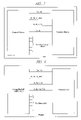
- FIG. 7 is a diagram showing an example in which a memory macro according to the present invention is mounted on an LSI.
- FIG. 8 is a diagram showing an example in which an integrated circuit device (memory LSI) according to the present invention is mounted on a board.
- an integrated circuit device memory LSI
- FIG. 1 shows a function block diagram of a synchronous memory circuit mounted on a semiconductor integrated circuit device.
- a bank 101 which is a unit operable independently each other is composed of a decoder 102 and a memory array 103 .
- 16 banks 101 - 0 to 101 - 15 ) are mounted.
- a read instruction signal /R a write instruction signal /W, a data rate instruction signal /F, and another instruction are inputted into a control circuit 104 controlling the synchronous memory circuit, and various control signals are supplied to a read circuit 106 and a write circuit 107 .
- the read circuit 106 and the write circuit 107 are provided commonly to a plurality of banks 101 - 1 to 101 - 15 .
- the read circuit 106 and the write circuit 107 are provided independently of each other, and both a read instruction and a write instruction can be received at one cycle as a synchronous memory circuit. Note that, in this case, the read instruction and the write instruction must be issued for different banks. Since data buses are also divided into a read system Q[35:0] and a write system D[35:0], read operation and write operation can be performed simultaneously with reception of instruction.
- the read circuit 106 includes an output register 108 temporarily storing read data from the memory array 103 of the bank 101 and a selector 109 selectively outputting the read data stored in the output register 108 to the read system data bus.
- the write circuit 107 includes an input register 110 temporarily storing write data from the write system data bus and a write buffer 111 storing data to be written in the memory array 103 of the bank 101 designated by addresses (BA, SA) of the write data stored in the input register 110 .
- the write data is taken in at SDR (single data rate) or at DDR (double data rate) according to polarity of a date rate instruction signal /F.
- SDR single data rate
- DDR double data rate
- serial-parallel conversion of 36:44 is performed when the burst length is 4
- serial-parallel conversion of 36:72 is performed when the burst length is 2
- write operation to the memory array is conducted.
- read data is read from the memory array 103 by 144 bits for one instruction and parallel-serial conversion of 144:36 is performed.
- An address register 112 stores a memory address to be accessed.
- the memory address is composed of a bank address BA and a synchronous address SA.
- the clock generating circuit 105 is composed of, for example, PLL, and includes two systems of basic clocks (K, /K) and output clocks (C, /C) in this configuration example. And, echo clocks (CQ, /CQ) are supplied to the outside of the synchronous memory circuit (see FIG. 6 ). Impedance control is performed to a clock (CQ, /CQ) driver and a driver to the read system data bus by an impedance control circuit 113 .
- FIGS. 2A and 2B show configuration examples of burst length control circuits (read/write) generating burst length control signals (read/write) RDBL4T/WRBL4T, respectively.
- the burst length control circuits are included in the control circuit 104 .
- FIG. 3 shows a timing chart of the burst length control signals (read/write) shown in FIGS. 2A and 2B .
- FIG. 3 shows a waveform of a burst length control signal (read) RDBL4T in the case where the read instruction signal /R is High at a first cycle, Low at a second to a fourth cycles and High again at a fifth cycle and later.
- a waveform of the burst length control signal (read) RDBL4T having Low at the first to the fourth cycles, High at the fifth cycle and Low again at a sixth cycle and later is outputted.
- the read instruction signal /R is High and read operation is not performed, that is, NOP (No Operation).
- the read instruction signal /R is Low and read operation is performed.
- the burst control signal (read) RDBL4T is Low and read operation of burst length 2 is performed. While the read instruction signal /R is continuously kept. Low (the second to the fourth cycles), the read operation of burst length 2 continues, and when the read instruction signal /R becomes High (the fifth cycle), the burst length control signal (read) RDBL4T becomes High and read operation of burst length 4 is performed. Since the read instruction signal /R is High, read operation to new address is not performed, but data having not been outputted of read data corresponding to the previous address is outputted since the burst length becomes 4, as a result, the data bus is occupied.
- the operation of the burst length control circuit (read) will be further explained using FIGS. 4A , 4 B and 4 C.
- the output register 108 has capacity of 144 bits in the configuration shown in FIG. 1 , and the capacity is divided into four regions each having 36 bits. In a case of read of burst length 2 , two regions are selected by the selector 109 and outputted to the read system data bus. Read data at the third to the fifth cycles shown in FIG. 3 will be explained in further detail. At the third cycle, upon reception of the read instruction signal /R (Low), A 3 to D 3 (each of A 3 to D 3 is read data of 36 bits) are read from the memory array and outputted to the output register 108 according to address signals (BA, SA).
- burst length control signal (read) RDBL4T since the burst length control signal (read) RDBL4T is Low, data of 72 bits which is read data (for example, A 3 and B 3 ) of two regions of the four regions is read and outputted to the data bus (the read of burst length 2 ).
- a 4 to D 4 (each of A 4 to D 4 is read data of 36 bits) are newly read from the memory array and outputted to the output register 108 according to address signals (BA, SA).
- the burst length control signal (read) RDBL4T since the burst length control signal (read) RDBL4T is Low, data of 72 bits which is read data (for example, A 4 and B 4 ) of two regions of the four regions is read and outputted to the data bus. Further, at the fifth cycle, upon reception of the read instruction signal /R (High), read from new memory array is not performed. Meanwhile, in the selector 109 , since the burst length control signal (read) RDBL4T is High, data of 72 bits which is read data (C 4 and D 4 in the abovementioned example) of the remaining two regions is read and outputted to the data bus. And thereby, the read of burst length 4 is realized.
- FIG. 3 shows a waveform of a burst length control signal (write) WRBL4T in a case where the write instruction signal /W is High at the first cycle, Low at the second to the fourth cycles and High again at the fifth cycle and later.
- a waveform of the burst length control signal (write) WRBL4T having High at the first to the second cycles, Low at the third to the fourth cycles and High again at the fifth cycle and later is outputted.
- the write instruction signal /W is High and write operation is not performed, that is, NOP (No Operation).
- write data is latched at each cycle so that the write operation can start whenever a write instruction is issued.
- the write instruction signal /W becomes Low at the second cycle
- the write operation is performed.
- the burst length control signal (write) WRBL4T is High and write operation of burst length 4 is performed.
- the burst length control signal (write) WRBL4T becomes Low (at the third and the fourth cycles) and write operation of burst length 2 is performed.
- the operation of the burst length control circuit (write) will be further explained using FIGS. 5A , 5 B and 5 C.
- the input register 110 has capacity of 144 bits in the configuration shown in FIG. 1 , and the capacity is divided into four regions each having 36 bits.
- Write data at the first to the third cycles shown in FIG. 3 will be explained in further detail.
- the write instruction signal /W is High
- write data a 1 and b 1 are latched.
- the write instruction signal /W becomes Low.
- write data c 1 and d 1 (each of cl and dl is write data of 36 bits) are latched, and 144 bits of write data a 1 to d 1 are transferred to the write buffer 111 and written in designated addresses (BA, SA) (write of burst length 4 ).
- write instruction signal /W is Low and the burst length control signal (write) WRBL4T is Low at the third cycle
- write data a 2 and b 2 are latched and 72 bits of the latched write data a 2 and b 2 are transferred to the write buffer 111 and written in designated addresses (BA, SA) (write of burst length 2 ). Switching of a range to be activated between 72 bits and 144 bits is performed according to input of the burst length control signal (write) WRBL4T into the write buffer 111 .
- the burst length to be switched should be set to be advantageous for performance improvement of a system using the synchronous memory circuit of the present invention.
- FIG. 6 shows an example of a timing chart of the synchronous memory circuit shown in FIG. 1 in simultaneous read and write.
- a data rate instruction signal /F is Low and a timing chart of operation at DDR is shown.
- a read instruction signal /R becomes Low at a cycle # 0 .
- a read instruction of bank address #B 0 to address #A 0 is issued.
- Read data corresponding to this read instruction is 2 bits (Q 0 a , Q 0 b ) from the second half of a cycle # 5 at DDR.
- the read instruction signal /R is Low and a read instruction is issued at cycle # 1 also, the read data corresponding to the read instruction at the cycle # 0 is only the abovementioned 2 bits (Q 0 a , Q 0 b ) at burst length 2 .
- a read instruction is issued to address #A 4 of bank address #B 4 at cycle # 2 , a read instruction is not issued at the next cycle # 3 , and therefore, the burst length becomes 4 and 4 bits (Q 4 a , Q 4 b , Q 4 c , Q 4 d ) are read from the second half of a cycle # 7 at DDR.
- the write instruction signal /W is also low and a write instruction is issued to address #A 1 of bank address #B 1 issued at the second half of the cycle # 0 . Since the write instruction signal /W is High at the previous cycle #( ⁇ 1), write operation of burst length 4 is performed and data of 4 bits (D 1 a , D 1 b , D 1 c , D 1 d ) is written from the cycle #( ⁇ 1) at DDR. Since the write instruction signal /W is Low at the next cycle # 1 also, the burst length becomes 2 and data of 2 bits (D 3 a , D 3 b ) is written from the cycle # 1 at DDR.
- FIG. 7 shows an example in which a memory macro according to the present invention is mounted on an LSI.
- FIG. 8 shows an example in which an integrated circuit device according to the present invention is mounted on a board.
- a control circuit and a memory macro corresponding to the configuration shown in FIG. 1 are integrated on one chip.
- the control circuit shown in FIG. 7 is integrated on a controller LSI of one chip, a memory LSI corresponding to the configuration shown in FIG. 1 is integrated on one chip, and these plural chips are mounted on the board.
- a control signal ( FIG. 7 ) from the control circuit to the memory macro or a control signal ( FIG. 8 ) from the controller LSI to the memory LSI is a control signal required for basic read or write operation shown in FIGS. 3 to 6 and a signal instructing burst length is not provided.
Landscapes
- Engineering & Computer Science (AREA)
- Microelectronics & Electronic Packaging (AREA)
- Computer Hardware Design (AREA)
- Dram (AREA)
- Static Random-Access Memory (AREA)
Abstract
Description
Claims (4)
Applications Claiming Priority (3)
| Application Number | Priority Date | Filing Date | Title |
|---|---|---|---|
| JP2006-293486 | 2006-10-30 | ||
| JPJP2006-293486 | 2006-10-30 | ||
| JP2006293486A JP4940894B2 (en) | 2006-10-30 | 2006-10-30 | Synchronous memory circuit |
Publications (2)
| Publication Number | Publication Date |
|---|---|
| US20080175091A1 US20080175091A1 (en) | 2008-07-24 |
| US7729198B2 true US7729198B2 (en) | 2010-06-01 |
Family
ID=39444926
Family Applications (1)
| Application Number | Title | Priority Date | Filing Date |
|---|---|---|---|
| US11/926,756 Expired - Fee Related US7729198B2 (en) | 2006-10-30 | 2007-10-29 | Synchronous memory circuit |
Country Status (2)
| Country | Link |
|---|---|
| US (1) | US7729198B2 (en) |
| JP (1) | JP4940894B2 (en) |
Cited By (1)
| Publication number | Priority date | Publication date | Assignee | Title |
|---|---|---|---|---|
| US20120106275A1 (en) * | 2010-10-29 | 2012-05-03 | Ok Sung-Hwa | Ringback circuit for semiconductor memory device |
Citations (5)
| Publication number | Priority date | Publication date | Assignee | Title |
|---|---|---|---|---|
| JP2000090665A (en) | 1998-08-07 | 2000-03-31 | Samsung Electronics Co Ltd | Synchronous type semiconductor memory |
| JP2000306379A (en) | 1999-04-16 | 2000-11-02 | Mitsubishi Electric Corp | Semiconductor memory |
| US6556506B2 (en) * | 1997-12-17 | 2003-04-29 | Fujitsu Limited | Memory access methods and devices for use with random access memories |
| US6674686B2 (en) * | 2001-04-18 | 2004-01-06 | Samsung Electronics Co., Ltd. | Method and apparatus for read operation and write operation in semiconductor memory device |
| US6999376B2 (en) * | 2000-08-25 | 2006-02-14 | Micron Technology, Inc. | Burst read addressing in a non-volatile memory device |
Family Cites Families (3)
| Publication number | Priority date | Publication date | Assignee | Title |
|---|---|---|---|---|
| JPH10208468A (en) * | 1997-01-28 | 1998-08-07 | Hitachi Ltd | Semiconductor memory and synchronous semiconductor memory |
| JP3251237B2 (en) * | 1998-05-29 | 2002-01-28 | 日本電気株式会社 | Reprogramming method in SDRAM |
| JP4108237B2 (en) * | 1999-11-04 | 2008-06-25 | 株式会社リコー | Memory control device |
-
2006
- 2006-10-30 JP JP2006293486A patent/JP4940894B2/en not_active Expired - Fee Related
-
2007
- 2007-10-29 US US11/926,756 patent/US7729198B2/en not_active Expired - Fee Related
Patent Citations (7)
| Publication number | Priority date | Publication date | Assignee | Title |
|---|---|---|---|---|
| US6556506B2 (en) * | 1997-12-17 | 2003-04-29 | Fujitsu Limited | Memory access methods and devices for use with random access memories |
| JP2000090665A (en) | 1998-08-07 | 2000-03-31 | Samsung Electronics Co Ltd | Synchronous type semiconductor memory |
| US6128233A (en) | 1998-08-07 | 2000-10-03 | Samsung Electronics, Co., Ltd. | Data transmission circuitry of a synchronous semiconductor memory device |
| JP2000306379A (en) | 1999-04-16 | 2000-11-02 | Mitsubishi Electric Corp | Semiconductor memory |
| US20010036116A1 (en) | 1999-04-16 | 2001-11-01 | Takashi Kubo | Semiconductor memory device capable of high speed input/output of wide bandwidth data by improving usage efficiency of external data bus |
| US6999376B2 (en) * | 2000-08-25 | 2006-02-14 | Micron Technology, Inc. | Burst read addressing in a non-volatile memory device |
| US6674686B2 (en) * | 2001-04-18 | 2004-01-06 | Samsung Electronics Co., Ltd. | Method and apparatus for read operation and write operation in semiconductor memory device |
Cited By (2)
| Publication number | Priority date | Publication date | Assignee | Title |
|---|---|---|---|---|
| US20120106275A1 (en) * | 2010-10-29 | 2012-05-03 | Ok Sung-Hwa | Ringback circuit for semiconductor memory device |
| US8441871B2 (en) * | 2010-10-29 | 2013-05-14 | Hynix Semiconductor Inc. | Ringback circuit for semiconductor memory device |
Also Published As
| Publication number | Publication date |
|---|---|
| US20080175091A1 (en) | 2008-07-24 |
| JP4940894B2 (en) | 2012-05-30 |
| JP2008112485A (en) | 2008-05-15 |
Similar Documents
| Publication | Publication Date | Title |
|---|---|---|
| JP5399442B2 (en) | Memory transaction burst operation and memory device supporting time multiplexed error correction coding | |
| KR100588599B1 (en) | Memory module and memory system | |
| US8284602B2 (en) | Pipe latch circuit of multi-bit prefetch-type semiconductor memory device with improved structure | |
| US6614700B2 (en) | Circuit configuration with a memory array | |
| US6895474B2 (en) | Synchronous DRAM with selectable internal prefetch size | |
| US7966446B2 (en) | Memory system and method having point-to-point link | |
| KR100711100B1 (en) | Memory module and memory system including the same | |
| US20080285372A1 (en) | Multi- port memory device for buffering between hosts and non-volatile memory devices | |
| EP1415304B1 (en) | Memory device having different burst order addressing for read and write operations | |
| US7596049B2 (en) | Semiconductor memory device with a plurality of bank groups each having a plurality of banks sharing a global line group | |
| US7356654B2 (en) | Flexible multi-area memory and electronic device using the same | |
| US7898880B2 (en) | Dual port memory device, memory device and method of operating the dual port memory device | |
| EP1028427B1 (en) | Hierarchical prefetch for semiconductor memories | |
| US7830740B2 (en) | Semiconductor memory device having selectable transfer modes | |
| JP2009104682A (en) | Semiconductor memory device and kind development method | |
| US7729198B2 (en) | Synchronous memory circuit | |
| KR100549171B1 (en) | Integrated memory using prefetch architecture and method for operating an integrated memory | |
| US7196962B2 (en) | Packet addressing programmable dual port memory devices and related methods | |
| US7230858B2 (en) | Dual frequency first-in-first-out structure | |
| JP4197285B2 (en) | Memory controller | |
| KR100596799B1 (en) | A device for distributing input data for memory device |
Legal Events
| Date | Code | Title | Description |
|---|---|---|---|
| AS | Assignment |
Owner name: HITACHI, LTD., JAPAN Free format text: ASSIGNMENT OF ASSIGNORS INTEREST;ASSIGNORS:HASEGAWA, MASATOSHI;NAKAYAMA, MICHIAKI;SAKAMOTO, MASATOSHI;REEL/FRAME:020046/0929 Effective date: 20071011 Owner name: HITACHI, LTD.,JAPAN Free format text: ASSIGNMENT OF ASSIGNORS INTEREST;ASSIGNORS:HASEGAWA, MASATOSHI;NAKAYAMA, MICHIAKI;SAKAMOTO, MASATOSHI;REEL/FRAME:020046/0929 Effective date: 20071011 |
|
| FEPP | Fee payment procedure |
Free format text: PAYOR NUMBER ASSIGNED (ORIGINAL EVENT CODE: ASPN); ENTITY STATUS OF PATENT OWNER: LARGE ENTITY |
|
| FPAY | Fee payment |
Year of fee payment: 4 |
|
| FEPP | Fee payment procedure |
Free format text: MAINTENANCE FEE REMINDER MAILED (ORIGINAL EVENT CODE: REM.) |
|
| LAPS | Lapse for failure to pay maintenance fees |
Free format text: PATENT EXPIRED FOR FAILURE TO PAY MAINTENANCE FEES (ORIGINAL EVENT CODE: EXP.) |
|
| STCH | Information on status: patent discontinuation |
Free format text: PATENT EXPIRED DUE TO NONPAYMENT OF MAINTENANCE FEES UNDER 37 CFR 1.362 |
|
| FP | Lapsed due to failure to pay maintenance fee |
Effective date: 20180601 |