US7710084B1 - Sample and hold technique for generating an average of sensed inductor current in voltage regulators - Google Patents
Sample and hold technique for generating an average of sensed inductor current in voltage regulators Download PDFInfo
- Publication number
- US7710084B1 US7710084B1 US12/077,463 US7746308A US7710084B1 US 7710084 B1 US7710084 B1 US 7710084B1 US 7746308 A US7746308 A US 7746308A US 7710084 B1 US7710084 B1 US 7710084B1
- Authority
- US
- United States
- Prior art keywords
- inductor current
- sensed
- current
- sensed inductor
- capacitor
- Prior art date
- Legal status (The legal status is an assumption and is not a legal conclusion. Google has not performed a legal analysis and makes no representation as to the accuracy of the status listed.)
- Active, expires
Links
- 238000000034 method Methods 0.000 title claims description 23
- 239000003990 capacitor Substances 0.000 claims abstract description 60
- 238000005070 sampling Methods 0.000 claims abstract description 7
- 230000008878 coupling Effects 0.000 claims description 4
- 238000010168 coupling process Methods 0.000 claims description 4
- 238000005859 coupling reaction Methods 0.000 claims description 4
- 101100328957 Caenorhabditis elegans clk-1 gene Proteins 0.000 description 5
- 238000010586 diagram Methods 0.000 description 3
- 230000008901 benefit Effects 0.000 description 2
- 230000000737 periodic effect Effects 0.000 description 2
- 230000000630 rising effect Effects 0.000 description 2
- 238000004088 simulation Methods 0.000 description 2
- 230000001105 regulatory effect Effects 0.000 description 1
- 230000001360 synchronised effect Effects 0.000 description 1
- 230000007704 transition Effects 0.000 description 1
Images


Classifications
-
- H—ELECTRICITY
- H02—GENERATION; CONVERSION OR DISTRIBUTION OF ELECTRIC POWER
- H02M—APPARATUS FOR CONVERSION BETWEEN AC AND AC, BETWEEN AC AND DC, OR BETWEEN DC AND DC, AND FOR USE WITH MAINS OR SIMILAR POWER SUPPLY SYSTEMS; CONVERSION OF DC OR AC INPUT POWER INTO SURGE OUTPUT POWER; CONTROL OR REGULATION THEREOF
- H02M3/00—Conversion of dc power input into dc power output
- H02M3/02—Conversion of dc power input into dc power output without intermediate conversion into ac
- H02M3/04—Conversion of dc power input into dc power output without intermediate conversion into ac by static converters
- H02M3/10—Conversion of dc power input into dc power output without intermediate conversion into ac by static converters using discharge tubes with control electrode or semiconductor devices with control electrode
- H02M3/145—Conversion of dc power input into dc power output without intermediate conversion into ac by static converters using discharge tubes with control electrode or semiconductor devices with control electrode using devices of a triode or transistor type requiring continuous application of a control signal
- H02M3/155—Conversion of dc power input into dc power output without intermediate conversion into ac by static converters using discharge tubes with control electrode or semiconductor devices with control electrode using devices of a triode or transistor type requiring continuous application of a control signal using semiconductor devices only
- H02M3/156—Conversion of dc power input into dc power output without intermediate conversion into ac by static converters using discharge tubes with control electrode or semiconductor devices with control electrode using devices of a triode or transistor type requiring continuous application of a control signal using semiconductor devices only with automatic control of output voltage or current, e.g. switching regulators
-
- G—PHYSICS
- G01—MEASURING; TESTING
- G01R—MEASURING ELECTRIC VARIABLES; MEASURING MAGNETIC VARIABLES
- G01R19/00—Arrangements for measuring currents or voltages or for indicating presence or sign thereof
- G01R19/003—Measuring mean values of current or voltage during a given time interval
-
- H—ELECTRICITY
- H02—GENERATION; CONVERSION OR DISTRIBUTION OF ELECTRIC POWER
- H02M—APPARATUS FOR CONVERSION BETWEEN AC AND AC, BETWEEN AC AND DC, OR BETWEEN DC AND DC, AND FOR USE WITH MAINS OR SIMILAR POWER SUPPLY SYSTEMS; CONVERSION OF DC OR AC INPUT POWER INTO SURGE OUTPUT POWER; CONTROL OR REGULATION THEREOF
- H02M1/00—Details of apparatus for conversion
- H02M1/0003—Details of control, feedback or regulation circuits
- H02M1/0009—Devices or circuits for detecting current in a converter
Definitions
- the present invention relates generally to electrical circuits, and more particularly but not exclusively to voltage regulators.
- a voltage regulator generates a regulated output voltage VOUT from an input voltage VIN. Ideally, the voltage regulator maintains the output voltage VOUT within regulation despite varying load current. However, this is not always the case in real world conditions.
- the output voltage VOUT of a practical voltage regulator may droop, i.e., decrease linearly, with changing load current.
- Droop control circuits have been developed to control output voltage droop. However, a droop control circuit must be able to accurately detect load current in order to control droop voltage.
- the present disclosure pertains to detecting the average of sensed inductor current, which may be used for droop control and other voltage regulator applications.
- a sample and hold inductor current sense configuration senses inductor current flowing through an output inductor of a voltage regulator and generates an average of the sensed inductor current.
- the average of the sensed inductor current may be generated from samples of peaks and valleys of the sensed inductor current.
- the peak of the sensed inductor current may be stored in a first capacitor and the valley of the sensed inductor current may be stored in a second capacitor.
- the first and second capacitors may be coupled together to generate the average of the sensed inductor current.
- the average of the sensed inductor current may be provided to a droop control circuit to control droop of an output voltage of the voltage regulator.
- An input offset voltage of a current sense amplifier sensing the inductor current may be calibrated between samplings of the sensed inductor current.
- FIG. 1 schematically shows the use of a sample and hold inductor current sense configuration in a voltage regulator in accordance with an embodiment of the present invention.
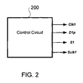
- FIG. 2 schematically shows a control circuit in accordance with an embodiment of the present invention.
- FIG. 3 shows waveforms of signals in the voltage regulator of FIG. 1 .
- FIG. 4 shows waveforms of signals in the voltage regulator of FIG. 1 in a simulation.
- FIG. 5 shows a flow diagram of a method of generating an average of sensed inductor current in a voltage regulator in accordance with an embodiment of the present invention.
- FIG. 1 schematically shows the use of a sample and hold inductor current sense configuration in a voltage regulator in accordance with an embodiment of the present invention.
- the inductor current sense configuration is employed in a low voltage, high current voltage regulator circuit 100 .
- the regulator circuit 100 may have multiple phases but circuitry for only one phase is shown in FIG. 1 for clarity of illustration.
- the inductor current sense configuration may also be employed in other voltage regulators without detracting from the merits of the present invention.
- switches S 4 and S 5 serve as synchronous switches of the regulator circuit 100 .
- An inverter 106 allows the switch S 4 to be ON (i.e., close) when the switch S 5 is driven OFF (i.e., open), and to be OFF when the switch S 5 is driven ON.
- the clock signal Clk 1 is a periodic signal that sets the SR flip-flop 105 at regular intervals to turn ON the top switch S 5 .
- the switches S 4 and S 5 may comprise MOSFET transistors, for example.
- the comparison signal COMP is indicative of the difference between the output voltage VOUT of the regulator circuit 100 at a node 102 and a reference voltage (not shown).
- the PWM (pulse width modulation) comparator 103 compares the comparison signal COMP to an emulated sensed inductor current at a node 112 to reset the flip-flop 105 , and thereby turn OFF the switch S 5 and turn ON the switch S 4 .
- the regulator circuit 100 includes an output inductor L and an output capacitor C 4 . Electrical current through the output inductor L is what is referred to as “inductor current.” The load is represented by the resistor R 1 and is coupled across the output capacitor C 4 . The inductor current charges the output capacitor C 4 to develop the output voltage VOUT.
- the resistor RL represents the DCR (DC resistance) of the output inductor L, which is also referred to as the “power inductor.”
- the input voltage VIN is the input voltage to the regulator 100 .
- the sample and hold inductor current sense configuration comprises a lossless current sense circuit 101 , a current sense amplifier 104 , and a sample and hold circuit 110 .
- the sample and hold inductor current sense configuration allows for sensing of the inductor current and generate its average.
- the sensed inductor current may be used for droop control, phase current balancing, and pulse width modulation when using current mode control.
- the lossless current sense circuit 101 comprises a sense resistor Rs and a sense capacitor Cs, which form an RC network across the output inductor L.
- the inductor current i.e., the current through the output inductor L
- the voltage across the sense capacitor Cs is thus equal to the inductor current multiplied by the resistor RL.
- the current sense amplifier 104 amplifies the voltage across the sense capacitor to generate a sense voltage ViL 1 representing the sensed inductor current.
- the valley i.e., lowest point
- the valley of the inductor current can be detected for cycle-by-cycle based peak/valley current mode control from the output of the current sense amplifier 104 .
- the resulting sensed inductor valley current is not accurate enough to be used for droop control due to valley-to-average inductor current error.
- This valley-to-average inductor current error also affects phase current balancing due to mismatched phase inductance.
- the voltage across the output capacitor Cs can be directly used for droop programming, it would be relatively difficult to calibrate input offset voltage of the current sense amplifier 104 using this approach because the signal from the output capacitor Cs is continuous.
- the sample and hold inductor current sense configuration of the present invention addresses these issues.
- the sample and hold circuit 110 includes capacitors C 1 and C 2 and switches S 1 , Sclk 1 , S 7 , and D 1 p .
- a control circuit 200 shown in FIG. 2 may generate the clock signal Clk 1 as well as the control signals for the switches S 1 , Sclk 1 , and D 1 p in accordance with the timing diagram shown in FIG. 3 .
- the clock signal Clk 1 is provided to the S input of the SR flip-flop 105 and controls a switch S 6 at the node 109 .
- the signal D 1 from the Q output of the SR flip-flop 105 controls the regulator top switch S 5 and the switch S 7 in the sample & hold circuit 110 .
- the control circuit 200 may be implemented using a variety of circuits without detracting from the merits of the present invention.
- the waveforms of FIG. 3 correspond to signals on nodes and components that are labeled the same in FIG. 1 .
- the operation of the sample and hold circuit 110 is now explained with reference to FIGS. 1 and 3 .
- the operation of the regulator circuit 100 is divided into time periods t 1 -t 2 , t 2 -t 3 , t 3 -t 4 , t 4 -t 5 , and t 5 -t 6 .
- time t 1 and time t 2 also referred to as a first sample window
- the peak of the sensed inductor current at the output of the current sense amplifier 104 is sampled to the capacitor C 1 right after the switch S 5 is turned OFF.
- Turning OFF the switch S 5 which is also referred to as the “top transistor,” results in the sensed inductor current going down as indicated by the ramping down of the voltage ViL 1 during the time period t 1 -t 2 .
- the peak, i.e., highest point, of the sensed inductor current may be sampled into the capacitor C 1 by turning ON the switch S 1 (see waveform “S 1 ” in FIG. 3 ), while the switches Sclk 1 , S 7 , and D 1 p are OFF.
- the voltage across the capacitor C 1 is shown in FIG. 3 as the waveform “VC 1 ”.
- input offset voltage calibration such as auto-zero calibration
- the current sense amplifier 104 can be done to further improve phase current sense and droop control accuracy.
- Any suitable conventional auto-zero calibration scheme for calibrating input offset voltage may be used without detracting from the merits of the present invention.
- Providing a time period for performing input offset voltage calibration is one of the benefits of using the sample and hold inductor current sense configuration of FIG. 1 .
- other methods of sensing the inductor current such as by using information directly from the sense capacitor Cs, does not readily allow for input offset voltage calibration of a current sense amplifier.
- the switch S 4 which is also referred to as the “bottom transistor,” continues to be ON (complete S 4 ON period is from t 1 to t 5 ) and the sensed peak inductor current is held by the capacitor C 1 (see 301 ).
- the inductor current which is represented by the voltage ViL 1 , ramps down towards its valley, i.e., its lowest point, during this time period (see 302 ).
- the valley of inductor valley current is sampled and held at the capacitor C 2 .
- the sampling of the valley of the inductor current may be performed at the second sample window defined by the pulse of a periodic clock signal applied at the switch Sclk 1 right before the switch S 6 or S 5 turns ON. Turning ON the switch Sckl 1 samples the valley of the inductor current and stores it at the capacitor C 2 .
- the voltage across the capacitor C 2 is shown in FIG. 3 as the waveform “VC 2 .”
- the clock signal Clk 1 turns ON the switch S 5 while the switches S 7 and S 6 are closed.
- the capacitor C 1 substantially the same size as the capacitor C 2 , and the size of each of the capacitors C 1 and C 2 is made much bigger than the capacitor C 3 (e.g., at least 10 ⁇ bigger)
- the voltage across the capacitor C 3 tracks the voltage across the capacitors C 1 and C 2 , and is equal to the average of the sensed inductor current.
- the voltage across the capacitor C 1 is shown as “VC 1 ”
- the voltage across the capacitor C 2 is shown as “VC 2 ”
- the voltage across the capacitor C 3 is shown as “VC 3 .”
- the average sensed inductor current may be provided to a droop control circuit (not shown). Such a droop control circuit may be electrically connected to the regulator 100 at the node 109 .
- the average sensed inductor current may also be used for multi-phase current balancing control. Any suitable conventional droop control and multi-phase current balancing control circuits may take advantage of the average sensed inductor current at the node 109 without detracting from the merits of the present invention.
- a current source 108 generates a ramp current iramp that is proportional to the difference between the input voltage VIN and the output voltage VOUT (i.e., VIN ⁇ VOUT) to emulate inductor current rising slope, plus an external compensation ramp slope for current mode control.
- switch D 1 p turns ON to allow the current source 108 to charge the capacitors C 1 and C 2 linearly to emulate sensed inductor current rising slope plus an external compensation slope (see 303 ).
- the emulated sensed inductor current is provided as an input to the PWM comparator 103 , which together with the clock signal Clk 1 at the S input of the flip-flop 105 , controls switching of the switches S 4 and S 5 to maintain the output voltage VOUT within regulation.
- FIG. 4 shows the voltage ViL 1 representing the sensed inductor current, the comparison signal COMP, the average sensed inductor current at the node 109 , the voltage VC 1 across the capacitor C 1 , and the voltage VC 2 across the capacitor C 2 in a simulation of the regulator circuit 100 of FIG. 1 .
- the horizontal axis represents time in microseconds, while the vertical axis represents magnitude in volts.
- the fluctuation in the comp signal between 150 and 165 microseconds represents a sudden load increase.
- the signal at the node 109 does not accurately represent the average of the inductor current.
- the signal at the node 109 quickly adapts to the change in the load and more accurately represents the average inductor current in the steady state period beginning around 170 microseconds.
- FIG. 5 there is shown a flow diagram of a method 500 of generating an average of sensed inductor current in a voltage regulator in accordance with an embodiment of the present invention.
- the method 500 may be performed using components shown in FIG. 1 , for example. Other components may also be used without detracting from the merits of the present invention.
- the sample and hold circuit 110 samples and holds the peak of a sensed inductor current at a first sample window.
- the sensed inductor current may be indicative of the inductor current flowing through the output inductor L.
- the inductor current may be sensed from the lossless current sense circuit 101 using the current sense amplifier 104 .
- step 502 the input offset voltage of the current sense amplifier 104 is calibrated at a time between the first sample window and a second sample window.
- step 503 the sample and hold circuit 110 samples and holds the valley of the sensed inductor current at the second sample window.
- an average of the sensed inductor current is generated from the sampled peak and valley of the sensed inductor current.
- the average sensed inductor current may be generated by coupling together capacitors C 1 and C 2 , which hold the peak and valley samples, respectively, of the sensed inductor current.
- step 505 the average of the sensed inductor current is used for droop control and multi-phase current balancing control of the regulator 100 .
- step 506 the sensed inductor current is emulated.
- An emulated sensed inductor current may be generated by charging the capacitors C 1 and C 2 with a ramp current that is proportional to the difference between the input voltage VIN and output voltage VOUT of the regulator 100 .
- step 507 the emulated sensed inductor current is used for current mode control of the regulator 100 .
Landscapes
- Physics & Mathematics (AREA)
- General Physics & Mathematics (AREA)
- Engineering & Computer Science (AREA)
- Power Engineering (AREA)
- Dc-Dc Converters (AREA)
Abstract
Description
L/RL=Rs*Cs, (EQ. 1)
where RL is the DCR of the output inductor L. The voltage across the sense capacitor Cs is thus equal to the inductor current multiplied by the resistor RL. The
C1=C2>>C3 (EQ. 1)
allows charge sharing between the capacitors C1 and C2, resulting in their voltage to be equal to the average of their voltages before the charge sharing. The voltage across the capacitor C3 tracks the voltage across the capacitors C1 and C2, and is equal to the average of the sensed inductor current. In
Claims (20)
Priority Applications (1)
| Application Number | Priority Date | Filing Date | Title |
|---|---|---|---|
| US12/077,463 US7710084B1 (en) | 2008-03-19 | 2008-03-19 | Sample and hold technique for generating an average of sensed inductor current in voltage regulators |
Applications Claiming Priority (1)
| Application Number | Priority Date | Filing Date | Title |
|---|---|---|---|
| US12/077,463 US7710084B1 (en) | 2008-03-19 | 2008-03-19 | Sample and hold technique for generating an average of sensed inductor current in voltage regulators |
Publications (1)
| Publication Number | Publication Date |
|---|---|
| US7710084B1 true US7710084B1 (en) | 2010-05-04 |
Family
ID=42124838
Family Applications (1)
| Application Number | Title | Priority Date | Filing Date |
|---|---|---|---|
| US12/077,463 Active 2028-06-07 US7710084B1 (en) | 2008-03-19 | 2008-03-19 | Sample and hold technique for generating an average of sensed inductor current in voltage regulators |
Country Status (1)
| Country | Link |
|---|---|
| US (1) | US7710084B1 (en) |
Cited By (54)
| Publication number | Priority date | Publication date | Assignee | Title |
|---|---|---|---|---|
| US20090327786A1 (en) * | 2008-06-26 | 2009-12-31 | Carroll Robert T | Power supply circuit and multi-phase control |
| US20100259996A1 (en) * | 2006-09-01 | 2010-10-14 | National Semiconductor Corporation | System and method for providing low cost high endurance low voltage electrically erasable programmable read only memory |
| US20110080209A1 (en) * | 2009-10-02 | 2011-04-07 | Power Integrations, Inc. | Method and apparatus for implementing slew rate control using bypass capacitor |
| US20110181199A1 (en) * | 2008-12-12 | 2011-07-28 | O2Micro, Inc. | Controllers, systems and methods for controlling dimming of light sources |
| US20110254537A1 (en) * | 2010-04-14 | 2011-10-20 | System General Corp. | Method and Apparatus for Detecting CCM Operation of a Magnetic Device |
| US20120153913A1 (en) * | 2010-12-20 | 2012-06-21 | Richtek Technology Corp | Method for improving voltage identification transient response and voltage regulator |
| CN102609021A (en) * | 2011-01-24 | 2012-07-25 | 立锜科技股份有限公司 | Method for improving voltage identification transient response and voltage regulator |
| US8288953B1 (en) * | 2010-01-19 | 2012-10-16 | Texas Instruments Incorporated | Buck constant average current regulation of light emitting diodes |
| US20120299502A1 (en) * | 2010-03-04 | 2012-11-29 | Yan Tiesheng | Circuits and methods for driving light sources |
| US20130009621A1 (en) * | 2011-07-07 | 2013-01-10 | Silergy Semiconductor Technology (Hangzhou) Ltd | Low offset, fast response voltage controlled current source and controlling method thereof |
| US20130015830A1 (en) * | 2011-07-11 | 2013-01-17 | Linear Technology Corporation | Switching Power Supply Having Separate AC And DC Current Sensing Paths |
| US8378588B2 (en) | 2008-12-12 | 2013-02-19 | O2Micro Inc | Circuits and methods for driving light sources |
| US8378589B2 (en) | 2008-12-12 | 2013-02-19 | O2Micro, Inc. | Driving circuit with dimming controller for driving light sources |
| US20130083566A1 (en) * | 2011-09-30 | 2013-04-04 | Power Integrations, Inc. | Multi-stage sampling circuit for a power converter controller |
| US20130082689A1 (en) * | 2011-09-29 | 2013-04-04 | Monolithic Power Systems, Inc. | Methods for sensing current in a switching regulator |
| US8482219B2 (en) | 2008-12-12 | 2013-07-09 | O2Micro, Inc. | Driving circuit with dimming controller for driving light sources |
| US8587275B2 (en) | 2011-02-09 | 2013-11-19 | National Semiconductor Corporation | Instantaneous average current measurement method |
| US8698419B2 (en) | 2010-03-04 | 2014-04-15 | O2Micro, Inc. | Circuits and methods for driving light sources |
| US20140103898A1 (en) * | 2012-10-17 | 2014-04-17 | Texas Instruments Incorporated | Apparatus and method for controlling inductor current in a switch mode power supply |
| US20140152281A1 (en) * | 2012-11-30 | 2014-06-05 | Yung-I Chang | Average inductor current mode voltage control device and method |
| US20140191736A1 (en) * | 2013-01-09 | 2014-07-10 | Infineon Technologies North America Corp. | Active Transient Response for DC-DC Converters |
| CN104009630A (en) * | 2013-02-22 | 2014-08-27 | 德州仪器公司 | Emulated current ramp for DC-DC converter |
| US8866398B2 (en) | 2012-05-11 | 2014-10-21 | O2Micro, Inc. | Circuits and methods for driving light sources |
| US20140320104A1 (en) * | 2013-02-22 | 2014-10-30 | Texas Instruments Incorporated | Advanced control circuit for switched-mode dc-dc converter |
| US20150077074A1 (en) * | 2011-12-27 | 2015-03-19 | International Rectifier Corporation | Circuit and Method for Producing an Average Output Inductor Current Indicator |
| TWI478476B (en) * | 2012-08-21 | 2015-03-21 | Alpha & Omega Semiconductor Cayman Ltd | Compensation of average inductor current control using variable reference voltage |
| US9030122B2 (en) | 2008-12-12 | 2015-05-12 | O2Micro, Inc. | Circuits and methods for driving LED light sources |
| US9035624B1 (en) * | 2011-12-27 | 2015-05-19 | International Rectifier Corporation | Power supply circuitry and current measurement |
| KR20150120187A (en) * | 2014-04-17 | 2015-10-27 | 삼성전자주식회사 | Dc-dc converter and electronic system comprising the same |
| US9232591B2 (en) | 2008-12-12 | 2016-01-05 | O2Micro Inc. | Circuits and methods for driving light sources |
| US9253843B2 (en) | 2008-12-12 | 2016-02-02 | 02Micro Inc | Driving circuit with dimming controller for driving light sources |
| US9356517B1 (en) * | 2014-12-01 | 2016-05-31 | Endura Technologies LLC | DC-DC converter with digital current sensing |
| US9386653B2 (en) | 2008-12-12 | 2016-07-05 | O2Micro Inc | Circuits and methods for driving light sources |
| US20170093385A1 (en) * | 2015-09-28 | 2017-03-30 | Cypress Semiconductor Corporation | Valley Detection Circuit and Drive Circuit |
| US9667156B2 (en) | 2015-03-06 | 2017-05-30 | Fairchild Semiconductor Corporation | Power supply with line compensation circuit |
| CN107134920A (en) * | 2016-05-20 | 2017-09-05 | 成都芯源系统有限公司 | Integrated circuit and method for controlling integrated circuit |
| US9780657B2 (en) * | 2015-07-21 | 2017-10-03 | Qualcomm Incorporated | Circuits and methods for controlling a boost switching regulator based on inductor current |
| US10123384B1 (en) | 2017-09-22 | 2018-11-06 | Linear Technology Holding, LLC | LED dimming |
| US10136488B1 (en) * | 2017-10-05 | 2018-11-20 | Linear Technology Holding, LLC | LED dimming |
| US20180351371A1 (en) * | 2014-11-13 | 2018-12-06 | Silergy Semiconductor Technology (Hangzhou) Ltd | Tuning circuit, tuning method and resonance-type contactless power supply |
| US20180375420A1 (en) * | 2017-03-24 | 2018-12-27 | Versatile Power, Inc. | Systems, methods, and devices for remote sense without wires |
| US10193442B2 (en) | 2016-02-09 | 2019-01-29 | Faraday Semi, LLC | Chip embedded power converters |
| US10201052B1 (en) | 2017-09-22 | 2019-02-05 | Linear Technology Holding, LLC | LED dimming |
| US10504848B1 (en) | 2019-02-19 | 2019-12-10 | Faraday Semi, Inc. | Chip embedded integrated voltage regulator |
| US10742202B1 (en) | 2019-07-23 | 2020-08-11 | International Business Machines Corporation | Autozero to an offset value for a slope detector for voltage droop monitoring |
| EP3732492A4 (en) * | 2017-12-29 | 2021-03-24 | Texas Instruments Incorporated | Apparatus and methods for processing sensed current |
| US11063516B1 (en) | 2020-07-29 | 2021-07-13 | Faraday Semi, Inc. | Power converters with bootstrap |
| US11069624B2 (en) | 2019-04-17 | 2021-07-20 | Faraday Semi, Inc. | Electrical devices and methods of manufacture |
| US11119126B2 (en) | 2019-07-23 | 2021-09-14 | International Business Machines Corporation | Slope detector for voltage droop monitoring |
| US11387731B2 (en) * | 2019-03-20 | 2022-07-12 | Texas Instruments Incorporated | DC-DC converter with improved regulation accuracy |
| US11469788B2 (en) * | 2018-11-27 | 2022-10-11 | Texas Instruments Incorporated | PS15 base current sampling in synchronous mode |
| GB2614089A (en) * | 2021-12-21 | 2023-06-28 | Cirrus Logic Int Semiconductor Ltd | Current estimation in a power converter |
| US11990839B2 (en) | 2022-06-21 | 2024-05-21 | Faraday Semi, Inc. | Power converters with large duty cycles |
| US11996770B2 (en) | 2022-11-23 | 2024-05-28 | Faraday Semi, Inc. | Chip embedded power converters |
Citations (31)
| Publication number | Priority date | Publication date | Assignee | Title |
|---|---|---|---|---|
| US4243975A (en) | 1977-09-30 | 1981-01-06 | Tokyo Shibaura Denki Kabushiki Kaisha | Analog-to-digital converter |
| US5852415A (en) | 1994-04-29 | 1998-12-22 | Analog Devices, Inc. | Charge redistribution analog-to-digital converter with system calibration |
| US6215288B1 (en) * | 2000-02-25 | 2001-04-10 | Cadence Design Systems, Inc. | Ultra-low power switching regulator method and apparatus |
| US6226419B1 (en) | 1999-02-26 | 2001-05-01 | Electronics For Imaging, Inc. | Automatic margin alignment using a digital document processor |
| US6320426B1 (en) | 2000-12-18 | 2001-11-20 | Topic Semiconductor Corp. | Self-calibrating circuit of high speed comparator |
| US6459335B1 (en) | 2000-09-29 | 2002-10-01 | Microchip Technology Incorporated | Auto-calibration circuit to minimize input offset voltage in an integrated circuit analog input device |
| US6515464B1 (en) | 2000-09-29 | 2003-02-04 | Microchip Technology Incorporated | Input voltage offset calibration of an analog device using a microcontroller |
| US6535061B2 (en) | 2000-12-06 | 2003-03-18 | Microchip Technology Incorporated | Configurable operational amplifier as a microcontroller peripheral |
| US6879136B1 (en) * | 2003-10-31 | 2005-04-12 | Analog Devices, Inc. | Inductor current emulation circuit for switching power supply |
| US7045993B1 (en) * | 2004-04-29 | 2006-05-16 | National Semiconductor Corporation | Apparatus and method for step-down switching voltage regulation |
| US7064528B2 (en) | 2004-03-11 | 2006-06-20 | Intersil Americas, Inc. | Droop amplifier circuit |
| US7064693B1 (en) | 2005-05-23 | 2006-06-20 | National Chiao Tung University | Background comparator offset calibration technique for flash analog-to-digital converters |
| US7133751B2 (en) | 2003-03-21 | 2006-11-07 | Intel Corporation | Method and apparatus for detecting on-die voltage variations |
| US7135836B2 (en) | 2003-03-28 | 2006-11-14 | Power Designers, Llc | Modular and reconfigurable rapid battery charger |
| US7158395B2 (en) | 2003-05-02 | 2007-01-02 | Ballard Power Systems Corporation | Method and apparatus for tracking maximum power point for inverters, for example, in photovoltaic applications |
| US7157924B2 (en) | 2001-12-19 | 2007-01-02 | Intel Corporation | Method and apparatus for on-die voltage fluctuation detection |
| US7164275B2 (en) | 2004-09-30 | 2007-01-16 | Rockwell Automation Technologies, Inc. | AC power line impedance monitoring method and system |
| US7170765B2 (en) | 2003-12-30 | 2007-01-30 | Delta Electronics, Inc. | Current distribution circuit |
| US7180919B2 (en) | 2002-08-23 | 2007-02-20 | Dainippon Screen Mfg. Co., Ltd. | Light emitting device drive circuit |
| US7202646B2 (en) | 2004-08-02 | 2007-04-10 | Vlt, Inc. | Control interface with droop compensation |
| US7225349B2 (en) | 2003-07-25 | 2007-05-29 | Intel Corporation | Power supply voltage droop compensated clock modulation for microprocessors |
| US7248082B2 (en) | 2004-11-30 | 2007-07-24 | Fujitsu Limited | Sample-hold circuit |
| US7256089B2 (en) | 2001-09-24 | 2007-08-14 | Intel Corporation | Top electrode barrier for on-chip die de-coupling capacitor and method of making same |
| US7274181B2 (en) | 2004-06-25 | 2007-09-25 | Intel Corporation | Systems, multiphase power converters with droop-control circuitry and methods |
| US7279869B2 (en) * | 2005-05-06 | 2007-10-09 | Aimtron Technology Corp. | PFM control circuit for DC regulator |
| USRE39976E1 (en) | 2001-11-26 | 2008-01-01 | Analog Devices, Inc. | Multi-phase switching regulator |
| US7339357B2 (en) | 2006-04-25 | 2008-03-04 | Agere Systems, Inc. | Power supply regulation using kelvin tap for voltage sense feedback from point within integrated circuit load |
| US7372241B1 (en) * | 2004-04-29 | 2008-05-13 | National Semiconductor Corporation | Apparatus and method for switching voltage regulation |
| US7432689B2 (en) * | 2006-05-05 | 2008-10-07 | Micrel, Inc. | Buck-boost control logic for PWM regulator |
| US7439716B2 (en) * | 2006-09-12 | 2008-10-21 | Semiconductor Components Industries, L.L.C. | DC-DC converter and method |
| US7492132B2 (en) * | 2005-08-11 | 2009-02-17 | Renesas Technology Corp. | Switching regulator |
-
2008
- 2008-03-19 US US12/077,463 patent/US7710084B1/en active Active
Patent Citations (33)
| Publication number | Priority date | Publication date | Assignee | Title |
|---|---|---|---|---|
| US4243975A (en) | 1977-09-30 | 1981-01-06 | Tokyo Shibaura Denki Kabushiki Kaisha | Analog-to-digital converter |
| US5852415A (en) | 1994-04-29 | 1998-12-22 | Analog Devices, Inc. | Charge redistribution analog-to-digital converter with system calibration |
| US6226419B1 (en) | 1999-02-26 | 2001-05-01 | Electronics For Imaging, Inc. | Automatic margin alignment using a digital document processor |
| US6215288B1 (en) * | 2000-02-25 | 2001-04-10 | Cadence Design Systems, Inc. | Ultra-low power switching regulator method and apparatus |
| US6459335B1 (en) | 2000-09-29 | 2002-10-01 | Microchip Technology Incorporated | Auto-calibration circuit to minimize input offset voltage in an integrated circuit analog input device |
| US6515464B1 (en) | 2000-09-29 | 2003-02-04 | Microchip Technology Incorporated | Input voltage offset calibration of an analog device using a microcontroller |
| US6535061B2 (en) | 2000-12-06 | 2003-03-18 | Microchip Technology Incorporated | Configurable operational amplifier as a microcontroller peripheral |
| US6320426B1 (en) | 2000-12-18 | 2001-11-20 | Topic Semiconductor Corp. | Self-calibrating circuit of high speed comparator |
| US7256089B2 (en) | 2001-09-24 | 2007-08-14 | Intel Corporation | Top electrode barrier for on-chip die de-coupling capacitor and method of making same |
| USRE39976E1 (en) | 2001-11-26 | 2008-01-01 | Analog Devices, Inc. | Multi-phase switching regulator |
| US7157924B2 (en) | 2001-12-19 | 2007-01-02 | Intel Corporation | Method and apparatus for on-die voltage fluctuation detection |
| US7180919B2 (en) | 2002-08-23 | 2007-02-20 | Dainippon Screen Mfg. Co., Ltd. | Light emitting device drive circuit |
| US7133751B2 (en) | 2003-03-21 | 2006-11-07 | Intel Corporation | Method and apparatus for detecting on-die voltage variations |
| US7135836B2 (en) | 2003-03-28 | 2006-11-14 | Power Designers, Llc | Modular and reconfigurable rapid battery charger |
| US7158395B2 (en) | 2003-05-02 | 2007-01-02 | Ballard Power Systems Corporation | Method and apparatus for tracking maximum power point for inverters, for example, in photovoltaic applications |
| US7225349B2 (en) | 2003-07-25 | 2007-05-29 | Intel Corporation | Power supply voltage droop compensated clock modulation for microprocessors |
| US6879136B1 (en) * | 2003-10-31 | 2005-04-12 | Analog Devices, Inc. | Inductor current emulation circuit for switching power supply |
| US7170765B2 (en) | 2003-12-30 | 2007-01-30 | Delta Electronics, Inc. | Current distribution circuit |
| US7064528B2 (en) | 2004-03-11 | 2006-06-20 | Intersil Americas, Inc. | Droop amplifier circuit |
| US7372241B1 (en) * | 2004-04-29 | 2008-05-13 | National Semiconductor Corporation | Apparatus and method for switching voltage regulation |
| US7119522B1 (en) * | 2004-04-29 | 2006-10-10 | National Semiconductor Corporation | Apparatus and method for step-down switching voltage regulation |
| US7372238B1 (en) * | 2004-04-29 | 2008-05-13 | National Semiconductor Corporation | Apparatus and method for step-down switching voltage regulation |
| US7045993B1 (en) * | 2004-04-29 | 2006-05-16 | National Semiconductor Corporation | Apparatus and method for step-down switching voltage regulation |
| US7274181B2 (en) | 2004-06-25 | 2007-09-25 | Intel Corporation | Systems, multiphase power converters with droop-control circuitry and methods |
| US7202646B2 (en) | 2004-08-02 | 2007-04-10 | Vlt, Inc. | Control interface with droop compensation |
| US7164275B2 (en) | 2004-09-30 | 2007-01-16 | Rockwell Automation Technologies, Inc. | AC power line impedance monitoring method and system |
| US7248082B2 (en) | 2004-11-30 | 2007-07-24 | Fujitsu Limited | Sample-hold circuit |
| US7279869B2 (en) * | 2005-05-06 | 2007-10-09 | Aimtron Technology Corp. | PFM control circuit for DC regulator |
| US7064693B1 (en) | 2005-05-23 | 2006-06-20 | National Chiao Tung University | Background comparator offset calibration technique for flash analog-to-digital converters |
| US7492132B2 (en) * | 2005-08-11 | 2009-02-17 | Renesas Technology Corp. | Switching regulator |
| US7339357B2 (en) | 2006-04-25 | 2008-03-04 | Agere Systems, Inc. | Power supply regulation using kelvin tap for voltage sense feedback from point within integrated circuit load |
| US7432689B2 (en) * | 2006-05-05 | 2008-10-07 | Micrel, Inc. | Buck-boost control logic for PWM regulator |
| US7439716B2 (en) * | 2006-09-12 | 2008-10-21 | Semiconductor Components Industries, L.L.C. | DC-DC converter and method |
Non-Patent Citations (6)
| Title |
|---|
| "6-Bit VID Controller 2-4 Phase VRM 10.X Controller", Jan. 5, 2004, pp. 1-30, FAN5019 Rev. 1.0.7, Fairchild Semiconductor Corporation. |
| "8-Bit Programmable 2 to 4 Phase Synchronous Buck Controller", Apr. 2006, pp. 1-6, FAN5032 Rev 1.0.0, Fairchild Semiconductor Corporation. |
| "8-Bit Programmable 2-to 5-Phase Synchronous Buck Controller", Jan. 2007, pp. 1-3, FAN5029 Rev. 1.1.3, Fairchild Semiconductor Corporation. |
| "8-Bit Programmable, 2 to 4 Phase, Synchronous Buck Controller", Mar. 2006, pp. 1-3, FAN5031 Rev. 1.0.1, Fairchild Semiconductor Corporation. |
| "8-Bit Programmable, 2-to 3-Phase Synchronous Buck Controller", Jan. 2007, pp. 1-39, FAN5033 Rev 1.0.0, Fairchild Semiconductor Corporation. |
| Forghani-Zadeh,H.S, et al. ,"Current-Sensing Techniques for DC-DC Converters", Published 2002, pp. 1-4, IEEE, Georgia Tech Analog Consortium, Georgia Institute of Technology, Atlanta, GA. |
Cited By (95)
| Publication number | Priority date | Publication date | Assignee | Title |
|---|---|---|---|---|
| US20100259996A1 (en) * | 2006-09-01 | 2010-10-14 | National Semiconductor Corporation | System and method for providing low cost high endurance low voltage electrically erasable programmable read only memory |
| US20090327786A1 (en) * | 2008-06-26 | 2009-12-31 | Carroll Robert T | Power supply circuit and multi-phase control |
| US8242759B2 (en) * | 2008-06-26 | 2012-08-14 | International Rectifier Corporation | Power supply circuit and multi-phase control based on peak and average current |
| US9386653B2 (en) | 2008-12-12 | 2016-07-05 | O2Micro Inc | Circuits and methods for driving light sources |
| US8482219B2 (en) | 2008-12-12 | 2013-07-09 | O2Micro, Inc. | Driving circuit with dimming controller for driving light sources |
| US9030122B2 (en) | 2008-12-12 | 2015-05-12 | O2Micro, Inc. | Circuits and methods for driving LED light sources |
| US20110181199A1 (en) * | 2008-12-12 | 2011-07-28 | O2Micro, Inc. | Controllers, systems and methods for controlling dimming of light sources |
| US9232591B2 (en) | 2008-12-12 | 2016-01-05 | O2Micro Inc. | Circuits and methods for driving light sources |
| US8378589B2 (en) | 2008-12-12 | 2013-02-19 | O2Micro, Inc. | Driving circuit with dimming controller for driving light sources |
| US8378588B2 (en) | 2008-12-12 | 2013-02-19 | O2Micro Inc | Circuits and methods for driving light sources |
| US9253843B2 (en) | 2008-12-12 | 2016-02-02 | 02Micro Inc | Driving circuit with dimming controller for driving light sources |
| US8508150B2 (en) | 2008-12-12 | 2013-08-13 | O2Micro, Inc. | Controllers, systems and methods for controlling dimming of light sources |
| US8970290B2 (en) | 2009-10-02 | 2015-03-03 | Power Integrations Inc. | Method and apparatus for implementing slew rate control using bypass capacitor |
| US8299772B2 (en) | 2009-10-02 | 2012-10-30 | Power Integrations, Inc. | Method and apparatus for implementing slew rate control using bypass capacitor |
| US20110080209A1 (en) * | 2009-10-02 | 2011-04-07 | Power Integrations, Inc. | Method and apparatus for implementing slew rate control using bypass capacitor |
| US8729882B2 (en) | 2009-10-02 | 2014-05-20 | Power Integrations, Inc. | Method and apparatus for implementing slew rate control using bypass capacitor |
| US8063622B2 (en) * | 2009-10-02 | 2011-11-22 | Power Integrations, Inc. | Method and apparatus for implementing slew rate control using bypass capacitor |
| US8288953B1 (en) * | 2010-01-19 | 2012-10-16 | Texas Instruments Incorporated | Buck constant average current regulation of light emitting diodes |
| US8664895B2 (en) * | 2010-03-04 | 2014-03-04 | O2Micro, Inc. | Circuits and methods for driving light sources |
| US20120299502A1 (en) * | 2010-03-04 | 2012-11-29 | Yan Tiesheng | Circuits and methods for driving light sources |
| US8698419B2 (en) | 2010-03-04 | 2014-04-15 | O2Micro, Inc. | Circuits and methods for driving light sources |
| US8890440B2 (en) | 2010-03-04 | 2014-11-18 | O2Micro, Inc. | Circuits and methods for driving light sources |
| US20110254537A1 (en) * | 2010-04-14 | 2011-10-20 | System General Corp. | Method and Apparatus for Detecting CCM Operation of a Magnetic Device |
| US8766617B2 (en) * | 2010-12-20 | 2014-07-01 | Richtek Technology Corp | Method for improving voltage identification transient response and voltage regulator |
| US20120153913A1 (en) * | 2010-12-20 | 2012-06-21 | Richtek Technology Corp | Method for improving voltage identification transient response and voltage regulator |
| CN102609021A (en) * | 2011-01-24 | 2012-07-25 | 立锜科技股份有限公司 | Method for improving voltage identification transient response and voltage regulator |
| CN102609021B (en) * | 2011-01-24 | 2014-09-03 | 立锜科技股份有限公司 | Method for improving voltage identification transient response and voltage regulator |
| US8587275B2 (en) | 2011-02-09 | 2013-11-19 | National Semiconductor Corporation | Instantaneous average current measurement method |
| US8710819B2 (en) * | 2011-07-07 | 2014-04-29 | Silergy Semiconductor Technology (Hangzhou) Ltd. | Low offset, fast response voltage controlled current source and controlling method thereof |
| US20130009621A1 (en) * | 2011-07-07 | 2013-01-10 | Silergy Semiconductor Technology (Hangzhou) Ltd | Low offset, fast response voltage controlled current source and controlling method thereof |
| TWI450068B (en) * | 2011-07-11 | 2014-08-21 | Linear Techn Inc | Switching power supply having separate ac and dc current sensing paths |
| US20130015830A1 (en) * | 2011-07-11 | 2013-01-17 | Linear Technology Corporation | Switching Power Supply Having Separate AC And DC Current Sensing Paths |
| US8823352B2 (en) * | 2011-07-11 | 2014-09-02 | Linear Technology Corporation | Switching power supply having separate AC and DC current sensing paths |
| US9817039B2 (en) * | 2011-09-29 | 2017-11-14 | Monolithic Power Systems, Inc. | Methods for sensing current in a switching regulator |
| US20130082689A1 (en) * | 2011-09-29 | 2013-04-04 | Monolithic Power Systems, Inc. | Methods for sensing current in a switching regulator |
| US8717785B2 (en) * | 2011-09-30 | 2014-05-06 | Power Integrations, Inc. | Multi-stage sampling circuit for a power converter controller |
| US20130083566A1 (en) * | 2011-09-30 | 2013-04-04 | Power Integrations, Inc. | Multi-stage sampling circuit for a power converter controller |
| US20150077074A1 (en) * | 2011-12-27 | 2015-03-19 | International Rectifier Corporation | Circuit and Method for Producing an Average Output Inductor Current Indicator |
| US9035624B1 (en) * | 2011-12-27 | 2015-05-19 | International Rectifier Corporation | Power supply circuitry and current measurement |
| US9502980B2 (en) * | 2011-12-27 | 2016-11-22 | Infineon Technologies Americas Corp. | Circuit and method for producing an average output inductor current indicator |
| US8866398B2 (en) | 2012-05-11 | 2014-10-21 | O2Micro, Inc. | Circuits and methods for driving light sources |
| TWI478476B (en) * | 2012-08-21 | 2015-03-21 | Alpha & Omega Semiconductor Cayman Ltd | Compensation of average inductor current control using variable reference voltage |
| US20140103898A1 (en) * | 2012-10-17 | 2014-04-17 | Texas Instruments Incorporated | Apparatus and method for controlling inductor current in a switch mode power supply |
| US9164528B2 (en) * | 2012-10-17 | 2015-10-20 | Texas Instruments Incorporated | Apparatus and method for controlling inductor current in a switch mode power supply |
| US20140152281A1 (en) * | 2012-11-30 | 2014-06-05 | Yung-I Chang | Average inductor current mode voltage control device and method |
| US8952669B2 (en) * | 2012-11-30 | 2015-02-10 | Alpha & Omega Semiconductor, Inc. | Average inductor current mode voltage control device and method |
| US20140191736A1 (en) * | 2013-01-09 | 2014-07-10 | Infineon Technologies North America Corp. | Active Transient Response for DC-DC Converters |
| US9998008B2 (en) * | 2013-01-09 | 2018-06-12 | Infineon Technologies Austria Ag | Active transient response for DC-DC converters |
| US9548651B2 (en) * | 2013-02-22 | 2017-01-17 | Texas Instruments Incorporated | Advanced control circuit for switched-mode DC-DC converter |
| US20170194862A1 (en) * | 2013-02-22 | 2017-07-06 | Texas Instruments Incorporated | Advanced Control Circuit for Switched-Mode DC-DC Converter |
| US9317049B2 (en) * | 2013-02-22 | 2016-04-19 | Texas Instruments Incorporated | Emulated current ramp for DC-DC converter |
| US20140320104A1 (en) * | 2013-02-22 | 2014-10-30 | Texas Instruments Incorporated | Advanced control circuit for switched-mode dc-dc converter |
| CN104009630A (en) * | 2013-02-22 | 2014-08-27 | 德州仪器公司 | Emulated current ramp for DC-DC converter |
| US20140239924A1 (en) * | 2013-02-22 | 2014-08-28 | Texas Instruments Incorporated | Emulated current ramp for dc-dc converter |
| KR20150120187A (en) * | 2014-04-17 | 2015-10-27 | 삼성전자주식회사 | Dc-dc converter and electronic system comprising the same |
| US9548661B2 (en) | 2014-04-17 | 2017-01-17 | Samsung Electronics Co., Ltd. | DC-DC converter and electronic system including the same |
| US20180351371A1 (en) * | 2014-11-13 | 2018-12-06 | Silergy Semiconductor Technology (Hangzhou) Ltd | Tuning circuit, tuning method and resonance-type contactless power supply |
| US11063443B2 (en) * | 2014-11-13 | 2021-07-13 | Silergy Semiconductor Technology (Hangzhou) Ltd | Tuning circuit, tuning method and resonance-type contactless power supply |
| US9712053B2 (en) | 2014-12-01 | 2017-07-18 | Endura Technologies LLC | DC-DC converter with digital current sensing |
| US10116214B2 (en) | 2014-12-01 | 2018-10-30 | Chaoyang Semiconductor Jiangyin Technology Co., Ltd. | DC-DC converter with digital current sensing |
| US9356517B1 (en) * | 2014-12-01 | 2016-05-31 | Endura Technologies LLC | DC-DC converter with digital current sensing |
| US9667156B2 (en) | 2015-03-06 | 2017-05-30 | Fairchild Semiconductor Corporation | Power supply with line compensation circuit |
| US9780657B2 (en) * | 2015-07-21 | 2017-10-03 | Qualcomm Incorporated | Circuits and methods for controlling a boost switching regulator based on inductor current |
| US9793883B2 (en) * | 2015-09-28 | 2017-10-17 | Cypress Semiconductor Corporation | Valley detection circuit and drive circuit |
| US20170093385A1 (en) * | 2015-09-28 | 2017-03-30 | Cypress Semiconductor Corporation | Valley Detection Circuit and Drive Circuit |
| JP2018532359A (en) * | 2015-09-28 | 2018-11-01 | サイプレス セミコンダクター コーポレーション | Valley detection circuit and drive circuit |
| CN107925355B (en) * | 2015-09-28 | 2019-08-02 | 赛普拉斯半导体公司 | Valley value detection circuit and driving circuit |
| WO2017058824A1 (en) * | 2015-09-28 | 2017-04-06 | Cypress Semiconductor Corporation | Valley detection circuit and drive circuit |
| CN107925355A (en) * | 2015-09-28 | 2018-04-17 | 赛普拉斯半导体公司 | Valley value detection circuit and drive circuit |
| US10193442B2 (en) | 2016-02-09 | 2019-01-29 | Faraday Semi, LLC | Chip embedded power converters |
| US11557962B2 (en) | 2016-02-09 | 2023-01-17 | Faraday Semi, Inc. | Chip embedded power converters |
| US10924011B2 (en) | 2016-02-09 | 2021-02-16 | Faraday Semi, Inc. | Chip embedded power converters |
| CN107134920B (en) * | 2016-05-20 | 2019-05-03 | 成都芯源系统有限公司 | Integrated circuit and method for controlling integrated circuit |
| CN107134920A (en) * | 2016-05-20 | 2017-09-05 | 成都芯源系统有限公司 | Integrated circuit and method for controlling integrated circuit |
| US9812963B1 (en) * | 2016-05-20 | 2017-11-07 | Monolithic Power Systems, Inc. | Current detection and averaging circuit for switching power supplies with a half-bridge switch circuit topology |
| US20180375420A1 (en) * | 2017-03-24 | 2018-12-27 | Versatile Power, Inc. | Systems, methods, and devices for remote sense without wires |
| US10666126B2 (en) * | 2017-03-24 | 2020-05-26 | Versatile Power, Inc. | Systems, methods, and devices for remote sense without wires |
| US10201052B1 (en) | 2017-09-22 | 2019-02-05 | Linear Technology Holding, LLC | LED dimming |
| US10123384B1 (en) | 2017-09-22 | 2018-11-06 | Linear Technology Holding, LLC | LED dimming |
| US10136488B1 (en) * | 2017-10-05 | 2018-11-20 | Linear Technology Holding, LLC | LED dimming |
| EP3732492A4 (en) * | 2017-12-29 | 2021-03-24 | Texas Instruments Incorporated | Apparatus and methods for processing sensed current |
| US11469788B2 (en) * | 2018-11-27 | 2022-10-11 | Texas Instruments Incorporated | PS15 base current sampling in synchronous mode |
| US10504848B1 (en) | 2019-02-19 | 2019-12-10 | Faraday Semi, Inc. | Chip embedded integrated voltage regulator |
| US11652062B2 (en) | 2019-02-19 | 2023-05-16 | Faraday Semi, Inc. | Chip embedded integrated voltage regulator |
| US11387731B2 (en) * | 2019-03-20 | 2022-07-12 | Texas Instruments Incorporated | DC-DC converter with improved regulation accuracy |
| US11069624B2 (en) | 2019-04-17 | 2021-07-20 | Faraday Semi, Inc. | Electrical devices and methods of manufacture |
| US11621230B2 (en) | 2019-04-17 | 2023-04-04 | Faraday Semi, Inc. | Electrical devices and methods of manufacture |
| US11119126B2 (en) | 2019-07-23 | 2021-09-14 | International Business Machines Corporation | Slope detector for voltage droop monitoring |
| US10742202B1 (en) | 2019-07-23 | 2020-08-11 | International Business Machines Corporation | Autozero to an offset value for a slope detector for voltage droop monitoring |
| US11063516B1 (en) | 2020-07-29 | 2021-07-13 | Faraday Semi, Inc. | Power converters with bootstrap |
| US11855534B2 (en) | 2020-07-29 | 2023-12-26 | Faraday Semi, Inc. | Power converters with bootstrap |
| GB2614089A (en) * | 2021-12-21 | 2023-06-28 | Cirrus Logic Int Semiconductor Ltd | Current estimation in a power converter |
| GB2614089B (en) * | 2021-12-21 | 2024-05-29 | Cirrus Logic Int Semiconductor Ltd | Current estimation in a power converter |
| US11990839B2 (en) | 2022-06-21 | 2024-05-21 | Faraday Semi, Inc. | Power converters with large duty cycles |
| US11996770B2 (en) | 2022-11-23 | 2024-05-28 | Faraday Semi, Inc. | Chip embedded power converters |
Similar Documents
| Publication | Publication Date | Title |
|---|---|---|
| US7710084B1 (en) | Sample and hold technique for generating an average of sensed inductor current in voltage regulators | |
| US10651754B1 (en) | Accurate peak detection architecture for secondary controlled AC-DC converter | |
| US9379623B2 (en) | Systems and methods for dynamic threshold adjustment with primary-side sensing and regulation for flyback power converters | |
| US9184651B2 (en) | Current detection and emulation circuit, and method thereof | |
| US9577537B2 (en) | Systems and methods for load compensation with primary-side sensing and regulation for flyback power converters | |
| US20210104949A1 (en) | Systems and methods of overvoltage protection for led lighting | |
| US7777457B2 (en) | Constant frequency current-mode buck-boost converter with reduced current sensing | |
| US7045993B1 (en) | Apparatus and method for step-down switching voltage regulation | |
| US10181792B2 (en) | Sensor-less buck current regulator with average current mode control | |
| US8120340B2 (en) | Control device for an interleaving power factor corrector | |
| EP2290795A1 (en) | Power supply controller with an input voltage compensation circuit | |
| US20150115923A1 (en) | Load current readback and average estimation | |
| US9841779B2 (en) | Variable reference signal generator used with switching mode power supply and the method thereof | |
| US20140062440A1 (en) | Sensorless Current Sense for Regulating Inductor Current in a Buck Converter | |
| US11990843B2 (en) | Methods and circuits for sensing isolated power converter output voltage across the isolation barrier | |
| US20240039384A1 (en) | Current detection circuit and controller for switching converter circuit | |
| CN112953181A (en) | Current detection circuit and method of fixed on-time power converter | |
| KR100839094B1 (en) | The circuit and method of sensing inductor current in dc/dc converter | |
| US11336168B2 (en) | Measuring current in a constant on-time regulator | |
| US20230353030A1 (en) | Current sampling in converter circuits | |
| JP2005049152A (en) | Current detecting circuit | |
| JP5578245B2 (en) | Constant current output control type switching regulator | |
| Straka | Multi-mode near minimum deviation controller IC for high frequency switch-mode power supplies | |
| CN112019045A (en) | Fixed open-time controller and buck converter device using the same | |
| CN103825433A (en) | Switch converter and control circuit thereof |
Legal Events
| Date | Code | Title | Description |
|---|---|---|---|
| AS | Assignment |
Owner name: FAIRCHILD SEMICONDUCTOR CORPORATION,MAINE Free format text: ASSIGNMENT OF ASSIGNORS INTEREST;ASSIGNOR:GUO, YIGANG;REEL/FRAME:024093/0888 Effective date: 20080318 |
|
| STCF | Information on status: patent grant |
Free format text: PATENTED CASE |
|
| FPAY | Fee payment |
Year of fee payment: 4 |
|
| AS | Assignment |
Owner name: DEUTSCHE BANK AG NEW YORK BRANCH, AS COLLATERAL AGENT, NEW YORK Free format text: PATENT SECURITY AGREEMENT;ASSIGNOR:FAIRCHILD SEMICONDUCTOR CORPORATION;REEL/FRAME:040075/0644 Effective date: 20160916 Owner name: DEUTSCHE BANK AG NEW YORK BRANCH, AS COLLATERAL AG Free format text: PATENT SECURITY AGREEMENT;ASSIGNOR:FAIRCHILD SEMICONDUCTOR CORPORATION;REEL/FRAME:040075/0644 Effective date: 20160916 |
|
| MAFP | Maintenance fee payment |
Free format text: PAYMENT OF MAINTENANCE FEE, 8TH YEAR, LARGE ENTITY (ORIGINAL EVENT CODE: M1552) Year of fee payment: 8 |
|
| AS | Assignment |
Owner name: SEMICONDUCTOR COMPONENTS INDUSTRIES, LLC, ARIZONA Free format text: ASSIGNMENT OF ASSIGNORS INTEREST;ASSIGNOR:FAIRCHILD SEMICONDUCTOR CORPORATION;REEL/FRAME:057694/0374 Effective date: 20210722 |
|
| MAFP | Maintenance fee payment |
Free format text: PAYMENT OF MAINTENANCE FEE, 12TH YEAR, LARGE ENTITY (ORIGINAL EVENT CODE: M1553); ENTITY STATUS OF PATENT OWNER: LARGE ENTITY Year of fee payment: 12 |
|
| AS | Assignment |
Owner name: FAIRCHILD SEMICONDUCTOR CORPORATION, ARIZONA Free format text: RELEASE BY SECURED PARTY;ASSIGNOR:DEUTSCHE BANK AG NEW YORK BRANCH;REEL/FRAME:057969/0206 Effective date: 20211027 |
|
| AS | Assignment |
Owner name: DEUTSCHE BANK AG NEW YORK BRANCH, AS COLLATERAL AGENT, NEW YORK Free format text: SECURITY INTEREST;ASSIGNOR:SEMICONDUCTOR COMPONENTS INDUSTRIES, LLC;REEL/FRAME:058871/0799 Effective date: 20211028 |
|
| AS | Assignment |
Owner name: FAIRCHILD SEMICONDUCTOR CORPORATION, ARIZONA Free format text: RELEASE OF SECURITY INTEREST IN PATENTS RECORDED AT REEL 040075, FRAME 0644;ASSIGNOR:DEUTSCHE BANK AG NEW YORK BRANCH, AS COLLATERAL AGENT;REEL/FRAME:064070/0536 Effective date: 20230622 Owner name: SEMICONDUCTOR COMPONENTS INDUSTRIES, LLC, ARIZONA Free format text: RELEASE OF SECURITY INTEREST IN PATENTS RECORDED AT REEL 040075, FRAME 0644;ASSIGNOR:DEUTSCHE BANK AG NEW YORK BRANCH, AS COLLATERAL AGENT;REEL/FRAME:064070/0536 Effective date: 20230622 |
|
| AS | Assignment |
Owner name: FAIRCHILD SEMICONDUCTOR CORPORATION, ARIZONA Free format text: RELEASE OF SECURITY INTEREST IN PATENTS RECORDED AT REEL 058871, FRAME 0799;ASSIGNOR:DEUTSCHE BANK AG NEW YORK BRANCH, AS COLLATERAL AGENT;REEL/FRAME:065653/0001 Effective date: 20230622 Owner name: SEMICONDUCTOR COMPONENTS INDUSTRIES, LLC, ARIZONA Free format text: RELEASE OF SECURITY INTEREST IN PATENTS RECORDED AT REEL 058871, FRAME 0799;ASSIGNOR:DEUTSCHE BANK AG NEW YORK BRANCH, AS COLLATERAL AGENT;REEL/FRAME:065653/0001 Effective date: 20230622 |