US7695890B2 - Negative photoresist for silicon KOH etch without silicon nitride - Google Patents

Negative photoresist for silicon KOH etch without silicon nitride Download PDF

Info

Publication number
US7695890B2
US7695890B2 US11/470,520 US47052006A US7695890B2 US 7695890 B2 US7695890 B2 US 7695890B2 US 47052006 A US47052006 A US 47052006A US 7695890 B2 US7695890 B2 US 7695890B2
Authority
US
United States
Prior art keywords
group
substrates
weight
individually selected
photosensitive layer
Prior art date
Legal status (The legal status is an assumption and is not a legal conclusion. Google has not performed a legal analysis and makes no representation as to the accuracy of the status listed.)
Active, expires
Application number
US11/470,520
Other versions
US20070075309A1 (en
Inventor
Xing-Fu Zhong
Jyoti K. Malhotra
Chenghong Li
Current Assignee (The listed assignees may be inaccurate. Google has not performed a legal analysis and makes no representation or warranty as to the accuracy of the list.)
Brewer Science Inc
Original Assignee
Brewer Science Inc
Priority date (The priority date is an assumption and is not a legal conclusion. Google has not performed a legal analysis and makes no representation as to the accuracy of the date listed.)
Filing date
Publication date
Priority to US11/470,520 priority Critical patent/US7695890B2/en
Application filed by Brewer Science Inc filed Critical Brewer Science Inc
Priority to KR1020087007155A priority patent/KR101360503B1/en
Priority to CN200680032665.4A priority patent/CN101258444B/en
Priority to JP2008530189A priority patent/JP4870769B2/en
Priority to PCT/US2006/034817 priority patent/WO2007030593A1/en
Priority to EP06803089A priority patent/EP1932060B1/en
Priority to TW095133184A priority patent/TWI411879B/en
Assigned to BREWER SCIENCE INC. reassignment BREWER SCIENCE INC. ASSIGNMENT OF ASSIGNORS INTEREST (SEE DOCUMENT FOR DETAILS). Assignors: MALHOTRA, JYOTI K., ZHONG, XING-FU, LI, CHENGHONG
Publication of US20070075309A1 publication Critical patent/US20070075309A1/en
Application granted granted Critical
Publication of US7695890B2 publication Critical patent/US7695890B2/en
Active legal-status Critical Current
Adjusted expiration legal-status Critical

Links

Classifications

    • GPHYSICS
    • G03PHOTOGRAPHY; CINEMATOGRAPHY; ANALOGOUS TECHNIQUES USING WAVES OTHER THAN OPTICAL WAVES; ELECTROGRAPHY; HOLOGRAPHY
    • G03FPHOTOMECHANICAL PRODUCTION OF TEXTURED OR PATTERNED SURFACES, e.g. FOR PRINTING, FOR PROCESSING OF SEMICONDUCTOR DEVICES; MATERIALS THEREFOR; ORIGINALS THEREFOR; APPARATUS SPECIALLY ADAPTED THEREFOR
    • G03F7/00Photomechanical, e.g. photolithographic, production of textured or patterned surfaces, e.g. printing surfaces; Materials therefor, e.g. comprising photoresists; Apparatus specially adapted therefor
    • G03F7/004Photosensitive materials
    • G03F7/038Macromolecular compounds which are rendered insoluble or differentially wettable
    • G03F7/0382Macromolecular compounds which are rendered insoluble or differentially wettable the macromolecular compound being present in a chemically amplified negative photoresist composition
    • GPHYSICS
    • G03PHOTOGRAPHY; CINEMATOGRAPHY; ANALOGOUS TECHNIQUES USING WAVES OTHER THAN OPTICAL WAVES; ELECTROGRAPHY; HOLOGRAPHY
    • G03FPHOTOMECHANICAL PRODUCTION OF TEXTURED OR PATTERNED SURFACES, e.g. FOR PRINTING, FOR PROCESSING OF SEMICONDUCTOR DEVICES; MATERIALS THEREFOR; ORIGINALS THEREFOR; APPARATUS SPECIALLY ADAPTED THEREFOR
    • G03F7/00Photomechanical, e.g. photolithographic, production of textured or patterned surfaces, e.g. printing surfaces; Materials therefor, e.g. comprising photoresists; Apparatus specially adapted therefor
    • G03F7/004Photosensitive materials
    • G03F7/0041Photosensitive materials providing an etching agent upon exposure
    • GPHYSICS
    • G03PHOTOGRAPHY; CINEMATOGRAPHY; ANALOGOUS TECHNIQUES USING WAVES OTHER THAN OPTICAL WAVES; ELECTROGRAPHY; HOLOGRAPHY
    • G03FPHOTOMECHANICAL PRODUCTION OF TEXTURED OR PATTERNED SURFACES, e.g. FOR PRINTING, FOR PROCESSING OF SEMICONDUCTOR DEVICES; MATERIALS THEREFOR; ORIGINALS THEREFOR; APPARATUS SPECIALLY ADAPTED THEREFOR
    • G03F7/00Photomechanical, e.g. photolithographic, production of textured or patterned surfaces, e.g. printing surfaces; Materials therefor, e.g. comprising photoresists; Apparatus specially adapted therefor
    • G03F7/004Photosensitive materials
    • G03F7/0045Photosensitive materials with organic non-macromolecular light-sensitive compounds not otherwise provided for, e.g. dissolution inhibitors
    • GPHYSICS
    • G03PHOTOGRAPHY; CINEMATOGRAPHY; ANALOGOUS TECHNIQUES USING WAVES OTHER THAN OPTICAL WAVES; ELECTROGRAPHY; HOLOGRAPHY
    • G03FPHOTOMECHANICAL PRODUCTION OF TEXTURED OR PATTERNED SURFACES, e.g. FOR PRINTING, FOR PROCESSING OF SEMICONDUCTOR DEVICES; MATERIALS THEREFOR; ORIGINALS THEREFOR; APPARATUS SPECIALLY ADAPTED THEREFOR
    • G03F7/00Photomechanical, e.g. photolithographic, production of textured or patterned surfaces, e.g. printing surfaces; Materials therefor, e.g. comprising photoresists; Apparatus specially adapted therefor
    • G03F7/004Photosensitive materials
    • G03F7/0047Photosensitive materials characterised by additives for obtaining a metallic or ceramic pattern, e.g. by firing
    • GPHYSICS
    • G03PHOTOGRAPHY; CINEMATOGRAPHY; ANALOGOUS TECHNIQUES USING WAVES OTHER THAN OPTICAL WAVES; ELECTROGRAPHY; HOLOGRAPHY
    • G03FPHOTOMECHANICAL PRODUCTION OF TEXTURED OR PATTERNED SURFACES, e.g. FOR PRINTING, FOR PROCESSING OF SEMICONDUCTOR DEVICES; MATERIALS THEREFOR; ORIGINALS THEREFOR; APPARATUS SPECIALLY ADAPTED THEREFOR
    • G03F7/00Photomechanical, e.g. photolithographic, production of textured or patterned surfaces, e.g. printing surfaces; Materials therefor, e.g. comprising photoresists; Apparatus specially adapted therefor
    • G03F7/004Photosensitive materials
    • G03F7/075Silicon-containing compounds
    • G03F7/0752Silicon-containing compounds in non photosensitive layers or as additives, e.g. for dry lithography
    • HELECTRICITY
    • H01ELECTRIC ELEMENTS
    • H01LSEMICONDUCTOR DEVICES NOT COVERED BY CLASS H10
    • H01L21/00Processes or apparatus adapted for the manufacture or treatment of semiconductor or solid state devices or of parts thereof
    • H01L21/02Manufacture or treatment of semiconductor devices or of parts thereof
    • H01L21/04Manufacture or treatment of semiconductor devices or of parts thereof the devices having at least one potential-jump barrier or surface barrier, e.g. PN junction, depletion layer or carrier concentration layer
    • H01L21/18Manufacture or treatment of semiconductor devices or of parts thereof the devices having at least one potential-jump barrier or surface barrier, e.g. PN junction, depletion layer or carrier concentration layer the devices having semiconductor bodies comprising elements of Group IV of the Periodic System or AIIIBV compounds with or without impurities, e.g. doping materials
    • H01L21/30Treatment of semiconductor bodies using processes or apparatus not provided for in groups H01L21/20 - H01L21/26
    • H01L21/302Treatment of semiconductor bodies using processes or apparatus not provided for in groups H01L21/20 - H01L21/26 to change their surface-physical characteristics or shape, e.g. etching, polishing, cutting
    • H01L21/306Chemical or electrical treatment, e.g. electrolytic etching
    • H01L21/308Chemical or electrical treatment, e.g. electrolytic etching using masks
    • H01L21/3081Chemical or electrical treatment, e.g. electrolytic etching using masks characterised by their composition, e.g. multilayer masks, materials
    • YGENERAL TAGGING OF NEW TECHNOLOGICAL DEVELOPMENTS; GENERAL TAGGING OF CROSS-SECTIONAL TECHNOLOGIES SPANNING OVER SEVERAL SECTIONS OF THE IPC; TECHNICAL SUBJECTS COVERED BY FORMER USPC CROSS-REFERENCE ART COLLECTIONS [XRACs] AND DIGESTS
    • Y10TECHNICAL SUBJECTS COVERED BY FORMER USPC
    • Y10STECHNICAL SUBJECTS COVERED BY FORMER USPC CROSS-REFERENCE ART COLLECTIONS [XRACs] AND DIGESTS
    • Y10S430/00Radiation imagery chemistry: process, composition, or product thereof
    • Y10S430/1053Imaging affecting physical property or radiation sensitive material, or producing nonplanar or printing surface - process, composition, or product: radiation sensitive composition or product or process of making binder containing
    • Y10S430/1055Radiation sensitive composition or product or process of making
    • Y10S430/106Binder containing
    • Y10S430/108Polyolefin or halogen containing
    • YGENERAL TAGGING OF NEW TECHNOLOGICAL DEVELOPMENTS; GENERAL TAGGING OF CROSS-SECTIONAL TECHNOLOGIES SPANNING OVER SEVERAL SECTIONS OF THE IPC; TECHNICAL SUBJECTS COVERED BY FORMER USPC CROSS-REFERENCE ART COLLECTIONS [XRACs] AND DIGESTS
    • Y10TECHNICAL SUBJECTS COVERED BY FORMER USPC
    • Y10STECHNICAL SUBJECTS COVERED BY FORMER USPC CROSS-REFERENCE ART COLLECTIONS [XRACs] AND DIGESTS
    • Y10S430/00Radiation imagery chemistry: process, composition, or product thereof
    • Y10S430/1053Imaging affecting physical property or radiation sensitive material, or producing nonplanar or printing surface - process, composition, or product: radiation sensitive composition or product or process of making binder containing
    • Y10S430/1055Radiation sensitive composition or product or process of making
    • Y10S430/114Initiator containing
    • Y10S430/115Cationic or anionic

Definitions

  • the present invention is concerned with new photoresists for use in the manufacture of microelectronic devices such as those used in microelectromechanical systems (MEMS).
  • MEMS microelectromechanical systems
  • etch protective coatings or masks for MEMS fabrication processes have been selected primarily by using a trial-and-error method because there are no general purpose protective coatings on the market.
  • the etch selectivity of the etchants to various materials is often used as a guide for MEMS process engineers.
  • films of silicon nitride have been used as a protective layer or hardmask during KOH or TMAH bulk silicon etching.
  • Silicon dioxide has a higher etch rate than silicon nitride, Therefore, it is only used as a protective/mask layer for very short etches.
  • Gold (Au), chromium (Cr), and boron (B) have also been reportedly used in some situations.
  • Non-patterned, hard-baked photoresists have been used as masks, but they are readily etched in alkaline solutions.
  • Polymethyl methacrylate was also evaluated as an etch mask for KOH. However, because of saponification of the ester group, the masking time of this polymer was found to decrease sharply from 165 minutes at 60° C. to 15 minutes at 90° C.
  • a photoresist layer to be patterned must be applied to the protective coating or mask so that the pattern can be transferred to the underlying substrate.
  • this can only be carried out after the protective coating or mask has been applied, thus requiring time and expense to apply and later etch this protective layer or mask, which is very difficult to remove.
  • the present invention overcomes these problems by providing spin-applied, photosensitive coating systems that replace prior art masks or protective coatings, and that eliminate the need for additional photoresists in the system.
  • the inventive systems protect device features from corrosion and other forms of attack during deep-etching processes that utilize concentrated aqueous bases.
  • the invention provides a photosensitive composition useful as a protective layer.
  • the composition comprises a polymer and a photoacid generator, and the polymer comprises styrene-containing monomers, acrylonitrile-containing monomers, and epoxy-containing monomers.
  • the invention also provides methods of using these photosensitive compositions in conjunction with a primer layer to form microelectronic structures.
  • these systems comprise a primer layer that is applied to a microelectronic substrate surface, and a photosensitive layer that is applied to the primer layer.
  • Preferred primer layers are formed from primer layer compositions including a silane dispersed or dissolved in a solvent system.
  • Aromatic and organo silanes are particularly preferred silanes for use in the primer layers of the invention.
  • the silane include at least one (and more preferably 2-3) group per mole of compound, or per repeat unit of polymer, that reacts with epoxy groups to form covalent bonds so that adhesion to a silicon substrate is very strong.
  • One preferred such group is an amine group.
  • Preferred silanes include aminoalkoxysilanes, preferably from about C 1 to about C 8 alkoxys, more preferably from about C 1 to about C 4 alkoxys, and even more preferably from about C 1 to about C 3 alkoxys.
  • the aminoalkoxysilane is an aminoalkylalkoxysilane, preferably from about C 1 to about C 8 alkyls, more preferably from about C 1 to about C 4 alkyls, and even more preferably from about C 1 to about C 3 alkyls.
  • Phenylaminoalkylalkoxysilanes are also preferred.
  • Some examples of the foregoing include aminopropyltrimethoxysilane, aminiopropyltriethoxysilane, N-phenylaminopropyltrimethoxysilane, N-phenylaminopropyltriethoxysilane, 3-glycidoxpropyltrimethoxysilane, 2-(3,4-epoxycyclohexyl)ethyltrimethoxysilane, and 3-mercaptopropyl-trimethoxysilane.
  • silanes include phenylsilanes such as phenyltrimethoxysilane, phenyltrichlorosilane, phenyltriethoxysilane, phenyltriacetoxysilane, and diphenylsilanes such as diphenyldimethoxysilane, diphenyldichlorosilane, and diphenylsilanediol.
  • phenylsilanes such as phenyltrimethoxysilane, phenyltrichlorosilane, phenyltriethoxysilane, phenyltriacetoxysilane
  • diphenylsilanes such as diphenyldimethoxysilane, diphenyldichlorosilane, and diphenylsilanediol.
  • the most preferred silanes include 2-phenylethyltrialkoxysilane p/m-chlorophenyltrimethoxysilane, p/m-bromophenyltrimethoxysilane, (pim-chloromethyl)phenyltrimethoxysilanie 2-(p/m-methoxy)phenylethyltrimethoxysilane, 2-(p/m-chloromethyl)phenylethyltrimethoxysilane, 3,4-dichlorophenyltnichlorosilane, 3-phenoxypropyltrichlorosilane, 3-(N-phenylamino)propyltnimethoxysilane, and 2-(diphenylphosphino)ethyltriethoxysilane.
  • An effective primer layer composition according to the invention is a mixture of a diphenyidialkoxysilane (e.g., diphenyldimethoxysilane) and a phenyltrialkoxysilane, (e.g., phenyltrimethoxysilane) or, even more preferably, a mixture of diphenylsilanediol and phenyltrimethoxysilane in a solution of 1 -methoxy-2-propanol or 1-propoxy-2-propanol with from about 5-10% by weight water.
  • a diphenyidialkoxysilane e.g., diphenyldimethoxysilane
  • a phenyltrialkoxysilane e.g., phenyltrimethoxysilane
  • a particularly effective primer layer composition for photosensitive layers comprising a poly(styrene-co-acrylonitrile) polymer is an alcohol and water solution containing from about 0.1-1.0% (preferably from about 0.25-0.5%) by weight diphenylsilanediol and from about 0.1-1.0% (preferably from about 0.25-0.5%) by weight of phenyltrimethoxysilane.
  • diphenylsilanediol and phenylsilanetriol the hydrolysis product of phenyltrimethoxysilane condense to from siloxane bonds and establish a three-dimensional silicone coating layer on the substrate.
  • Another preferred silane has the formula
  • Silanes having this structure are not only compatible with styrene-containing copolymers, but they are also reactive with ester, benzyl chloride, and/or epoxy groups, and they are excellent adhesion promoters.
  • One particularly preferred silane within the scope of this formula is
  • This silane is 3-[N-phenylamino]propyltrimetlioxysilane (mentioned above), and it is commercially available from Lancaster Synthesis and Gelest Corporation.
  • the silane should be included in the primer layer composition at a level of from about 0.1% to about 3% by weight, preferably from about 0.2% to about 2% by weight, and even more preferably from about 0.5% to about 1% by weight, based upon the total weight of solids in the primer layer composition taken as 100% by weight
  • the solvent system utilized in the primer layer composition should have a boiling point of from about 100° C. to about 220° C., and preferably from about 140° C. to about 180° C.
  • the solvent system should be utilized at a level of from about 30% to about 99.9% by weight, and preferably from about 40% to about 80% by weight, based upon the total weight of the primer layer composition taken as 100% by weight.
  • Preferred solvent systems include a solvent selected from the group consisting of methanol, ethanol, isopropanol, butanol, 1-methoxy-2-propanol, ethylene glycol monomethyl ether, and 1-propoxy-2-propanol, and mixtures thereof.
  • water is included in the solvent system at a level of from about 20% to about 60% by weight, and preferably from about 20% to about 40% by weight, based upon the total weight of the primer layer composition taken as 100% by weight.
  • the primer layer composition can also include a catalyst.
  • Suitable catalysts include any inorganic or organic acid (e.g., hydrochloric acid, sulfuric acid, phosphoric acid, acetic acid) or an inorganic or organic base (e.g., potassium hydroxide, TMAH, ammonia, amines).
  • the catalyst is preferably present in the primer layer composition at levels of from about 0.01% to about 0.5% by weight, more preferably from about 0.1% to about 0.3% by weight, and even more preferably from about 0.02% to about 0.03% by weight, based upon the total weight of solids in the primer layer composition taken as 100% by weight.
  • the primer layer can also include a number of optional ingredients, such as a surfactant.
  • a surfactant such as FC4430 (available from 3M) or Triton X-100 (available from 3M) can be added to make a uniform primer coating that is defect-free.
  • the photosensitive layer is formed from a composition comprising a polymer dispersed or dissolved in a solvent system.
  • a preferred polymer is a terpolymer comprising recurring: styrene monomers; acrylonitrile monomers; and monomers comprising functional groups that react with amines.
  • Preferred styrene monomers have the formula
  • Preferred acrylonitrile monomers have the formula
  • Preferred monomers comprising functional groups for reacting with amines include monomers comprising one or more epoxy groups (e.g., glycidyl methacrylate, glycidyl acrylate, vinylbenzoyl glycidyl ether).
  • epoxy groups e.g., glycidyl methacrylate, glycidyl acrylate, vinylbenzoyl glycidyl ether.
  • the polymer preferably comprises from about 35% to about 75% by weight of monomer (I), more preferably from about 40% to about 70% by weight of monomer (I), and even more preferably from about 50% to about 65% by weight of monomer (I).
  • the polymer preferably comprises from about 20% to about 40% by weight of monomer (II), more preferably from about 25% to about 35% by weight of monomer (II), and even more preferably from about 25% to about 30% by weight of monomer (II).
  • the polymer preferably comprises from about 5% to about 15% by weight of monomer (III), more preferably from about 6% to about 12% by weight of monomer (III), and even more preferably from about 8% to about 10% by weight of monomer (III).
  • Each of the above percentages by weight is based upon the total weight of the polymer taken as 100% by weight.
  • the polymer have a weight average molecular weight of from about 10,000 Daltons to about 80,000 Daltons, preferably from about 20,000 Daltons to about 60,000 Daltons, and even more preferably from about 30,000 Daltons to about 50,000 Daltons.
  • Monomers other than monomers (I), (II), and (III) can also be present in the polymer, if desired.
  • the combined weight of monomers (I), (II), and (III) in the polymer is preferably at least about 60% by weight, and more preferably from about 70% to about 90% by weight, based upon the total weight of the polymer taken as 100% by weight.
  • suitable other monomers include those having functional groups that can react with groups in the primer layer for achieving chemical bonding between the two layers.
  • These monomers may have, by way of example, haloalkyl (e.g., benzyl chloride, 2-chloroethyl methacrylate), ester (methacrylates, acrylates, maleates, fumarates, isocyanates), or anhydride functional groups, which react readily with functional groups such as hydroxyl, amino, or oxiranyl groups that can be present in the primer layer.
  • haloalkyl e.g., benzyl chloride, 2-chloroethyl methacrylate
  • ester methacrylates, acrylates, maleates, fumarates, isocyanates
  • anhydride functional groups which react readily with functional groups such as hydroxyl, amino, or oxiranyl groups that can be present in the primer layer.
  • the polymer should be included in the photosensitive layer composition at a level of from about 90% to about 98% by weight, and preferably from about 90% to about 95% by weight, based upon the total weight of solids in the photosensitive layer composition taken as 100% by weight.
  • the photosensitive composition will also comprise a photoacid generator (PAG).
  • PAG photoacid generator
  • the PAG generates a strong acid or superacid when exposed to actinic radiation such as UV light.
  • suitable PAGs include those selected from the group consisting of triarylsulfonium hexafluoroantimonate, triarylulfonium hexafluorophosphate, diaryliodonium hexafluoroantimonate, diaryliodonium hexafluorophosphate,
  • each R 3 is individually selected from the group consisting of C 3 H 7 , C 8 H 17 , CH 3 C 6 H 4 , and camphor.
  • the PAGs of formulas (IV) and (V) are sold by Ciba Specialty Chemicals as The CGI 13XX Family and The CGI 26X Family, respectively.
  • the PAG should be included in the photosensitive composition at a level of from about 2% to about 10% by weight, and preferably from about 5% to about 8% by weight, based upon the total weight of solids in the photosensitive composition taken as 100% by weight.
  • the solvent system utilized in the photosensitive composition should have a boiling point of from about 120° C. to about 200° C., and preferably from about 130° C. to about 180° C.
  • the solvent system should be utilized at a level of from about 70% to about 95% by weight, and preferably from about 80% to about 90% by weight, based upon the total weight of the photosensitive composition taken as 100% by weight.
  • Preferred solvent systems include a solvent selected from the group consisting of methyl isoamyl ketone, di(ethylene glycol) dimethyl ether, propylene glycol monomethyl ether acetate, ethyl lactate, cyclohexanone, and mixtures thereof.
  • Preferred substrates for use in this process include those comprising silicon.
  • Some particularly preferred substrates are selected from the group consisting of Si substrates, SiO 2 substrates, Si 3 N 4 substrates, SiO 2 on silicon substrates, Si 3 N 4 on silicon substrates, glass substrates, quartz substrates, ceramic substrates, semiconductor substrates, and metal substrates.
  • the silane and any other components are dissolved in the primer solvent system to form the silane composition.
  • This composition is then spin-applied onto the substrate at about 500-5,000 rpm, and preferably from about 1000-3,000 rpm, for about 30-90 seconds, and preferably for about 60 seconds. It is then baked at a temperature of from about 60-110° C. for about 60-180 seconds (preferably about 120 seconds), and then at about 150-250° C. for about 60-180 seconds (preferably about 120 seconds) in order to condense the silane molecules into a continuous film that is bonded to surface hydroxyl groups present on typical microelectronic substrates. That is, the hydrolyzed silane reacts with the silanol groups present in the silicon-containing substrate and also self-crosslinks by condensation.
  • the primer layer have an average thickness (as measured by an ellipsometer over 5 different points) of less than about 50 nm and more preferably from about 20 nm to about 30 nm.
  • the polymer, PAG, and any other components are dissolved in the solvent system and spin coated onto the substrate at about 1,000-5,000 rpm, and preferably from about 1,000-2,000 rpm, for about 30-90 seconds, and preferably about 60 seconds. It is then baked at a temperature of from about 100-120° C. for about 60-180 seconds (preferably about 120 seconds).
  • the polymer solids level and spinning conditions are typically adjusted to achieve an average coating thickness after baking (as measured by an ellipsometer over 5 different points) of from about 500 nm to about 3,000 nm, and preferably from about 1,000 nm to about 2,000 nm, depending upon the degree of coverage required over device topography on the substrate.
  • the epoxy or other reactive group in the photosensitive layer polymer form covalent bonds with an amine or other reactive group on the silane of the primer layer.
  • the photosensitive layer is then imaged by exposing it to UV light with a wavelength of from about 150-500 nm (e.g., about 248 nm or about 365 nm), preferably in a dose of about 500 mJ/cm 2 .
  • the coating is then preferably post-exposure baked at about 110° C. to about 30° C. for about 2 minutes, and developed with a solvent for about 1 minute. Finally, the coating is baked at about 200° C. to about 250° C. for about 5 minutes.
  • Exposure to light causes the PAG to generate an acid, and this acid initiates crosslinking of the polymer (preferably via the epoxy groups) in the photosensitive layer.
  • the crossliniked epoxy groups will have the structure
  • the exposed areas become substantially insoluble (e.g., less than about 1% by weight soluble, preferably less than about 0.05% soluble, and more preferably about 0% soluble) in typical solvent developers such as propylene glycol monomethyl ether acetate, methyl isoamyl ketone, and ethyl acetoacetate.
  • solvent developers such as propylene glycol monomethyl ether acetate, methyl isoamyl ketone, and ethyl acetoacetate.
  • the unexposed areas remain soluble in these developers and are thus readily removed during developing.
  • the pattern can be easily transferred with no additional etching steps to remove the protective layer being needed.
  • the layer systems will exhibit less than about 100 ⁇ m, preferably less than about 70 ⁇ m, and more preferably less than about 50 ⁇ m of undercutting when subjected for about 2 hours (or even about 3 hours) to etching in an approximately 30-35% by weight aqueous KOH solution having a temperature of about 83-87° C. Undercutting is determined by measuring the width of overhanging protective layer at the edge of etched areas as observed under a confocal microscope. 5 Furthermore, the inventive protective systems will experience very little or no etchant penetration during etching processes.
  • the inventive protective systems when subjected for about 2 hours (or even about 3 hours) to etching in an approximately 30-35% by weight aqueous KOH solution having a temperature of about 83-87 ° C., the inventive protective systems will have less than about 0.1 pinholes per cm 2 of substrate, and preferably less than about 0.05 pinholes per cm 2 of substrate, when observed under a microscope at 10 ⁇ magnification. This is different from prior art photosensitive layers, which would dissolve relatively quickly in KOH and thus required the presence of a separate protective layer such as a silicon nitride layer.
  • a solution was made by dissolving 67.50 g of styrene, 25.00 g of acrylonitrile, 7.50 g of glycidyl methacrylate, and 1.25 g of 2,2′-azobisisobutyronitrile in 400 g of cyclopentanone, all of which were obtained from Aldrich.
  • the solution was heated to 65° C. under nitrogen while undergoing magnetic stirring.
  • the polymerization was allowed to proceed at 65° C. for 98 hours.
  • the actual yield was determined by solids analysis to be 97% of the theoretical yield.
  • N-phenylaminopropyltrimethoxysilane obtained from Gelest
  • propylene glycol propyl ether obtained from General Chemical
  • the primer solution in Part 3 of this Example was spin coated onto a silicon wafer at 1,500 rpm for 1 minute.
  • the primer coating was baked at 75° C. for 2 minutes and then at 180° C. for 2 minutes.
  • the topcoat solution of Part 2 of this Example was then spin coated over the primer layer at 1,500 rpm for 1 minute.
  • the topcoat was baked at 100° C. for 2 minutes.
  • the coating was imaged by exposing it to UV light at 2)0 a wavelength of 365 nm in a dose of 500 mJ/cm 2 , baking at 130° C. for 2 minutes, and developing with acetone for 1 minute. Finally, the combination was baked at 230° C. for 5 minutes. A negative pattern was obtained.
  • the wafer prepared and patterned in Part 4 of this Example was etched in 30% KOH aqueous solution at 85° C. for 1 hour.
  • the silicon was etched 70 ⁇ m deep in areas without the polymer coating.
  • the polymer-coated areas remained intact.
  • the pattern was transferred to the silicon wafer in essentially the same manner as is the case with prior art silicon nitride masking methods.
  • a solution was made by dissolving 27.07 g of styrene, 10.00 g of acrylonitrile, 3.08 g of glycidyl methacrylate, and 0.51 g of dicumyl peroxide (obtained from Aldrich) in 160 g of PGMEA.
  • the solution was heated to 120° C. under nitrogen while undergoing magnetic stirring.
  • the polymerization was allowed to proceed at 120° C. for 24 hours.
  • the actual yield was determined by solids analysis to be 95.5% of the theoretical yield.
  • the primer solution of Part 2 of Example 1 was spin coated onto a silicon wafer at 1,500 rpm for 1 minute.
  • the primer coating was baked at 60° C. for 5 minutes and at 180° C. for 2 minutes.
  • the topcoat solution from Part 2 of this Example was then spin coated onto the wafer at 1,500 rpm for 1 minute.
  • the topcoat was baked at 100° C. for 2 minutes.
  • After the coating was imaged by exposing it to UV light at 254 nm in a dose of 500 mJ/cm 2 , it was baked at 130° C. for 2 minutes and then developed with PGMEA for 1 minute.
  • the coating was finally baked at 230 ° C. for 5 minutes. A negative pattern was obtained.
  • the wafer prepared and patterned in Part 3 of this Example was etched in 30% KOH aqueous solution at 80° C. for 1 hour.
  • the silicon was etched 58 ⁇ m deep in the areas without the polymer coating.
  • the polymer-coated areas remained intact
  • the pattern was transferred to the silicon wafer in essentially the same way as with prior art silicon nitride masking methods.
  • a solution was made by dissolving 168.0 g of styrene, 84.0 g of acrylonitrile, 28.3 g of glycidyl methacrylate, and 7.0 g of dicumyl peroxide in 1,120 g of PGMEA.
  • the solution was heated to 120° C. under nitrogen while undergoing magnetic stirring.
  • the polymerization was allowed to proceed at 120° C. for 28 hours.
  • the actual yield was found by solid analysis to be 97.5% of the theoretical.
  • the terpolymer was precipitated in isopropanol, filtered, and dried overnight under vacuum at 50° C.
  • N-phenylaminopropyltrimethoxysilane were dissolved in a mixture of 77.50 g of propylene glycol propyl ether (PnP), 120.14 g of deionized water, 0.51 g of acetic acid, and 0.03 g of FC4430 (a surfactant).
  • PnP propylene glycol propyl ether
  • FC4430 a surfactant
  • the primer solution prepared in Part 3 of this Example was spin coated onto a silicon wafer at 1,500 rpm for 1 minute.
  • the primer coating was baked at 100° C. for 1 minute and then at 205 ° C. for 1 minute.
  • the topcoat solution from Part 2 of this Example was spin coated over the primer layer at 1,500 rpm for I minute.
  • the topcoat was baked at 110° C. for 2 minutes.
  • the coating was imaged by exposing it to UV light at a wavelength of 365 nm in a dose of 500 mJ/cm 2 , baking at 130 ° C. for 2 minutes, and developing with PGMEA for 1 minute. Finally, the combination was baked at 230° C. for 5 minutes. A negative pattern was obtained.
  • the wafer prepared and patterned in Part 4 of this Example was etched in 30% KOH aqueous solution at 75° C. for 4 hours.
  • the silicon was etched 178 ⁇ m deep in the areas without the polymer coating.
  • the polymer-coated area remained intact.
  • the pattern was transferred to the silicon wafer in essentially the same manner as prior art silicon nitride masking methods.

Abstract

New photoresists for use during the production of semiconductor and MEMS devices are provided. The primer layer preferably comprises a silane dissolved or dispersed in a solvent system. The photoresist layer includes copolymers prepared from styrene, acrylonitrile, and epoxy-containing monomers. The photoresist layer comprises a photoacid generator, and is preferably negative-acting.

Description

RELATED APPLICATIONS
This applications claims the priority benefit of U.S. Patent Application No. 60/715,964, filed Sep. 9, 2005, entitled NEGATIVE PHOTORESIST FOR SILICON KOH ETCH WITHOUT SILICON NITRIDE, incorporated by reference herein.
BACKGROUND OF THE INVENTION
1. Field of the Invention
The present invention is concerned with new photoresists for use in the manufacture of microelectronic devices such as those used in microelectromechanical systems (MEMS).
2. Description of the Prior Art
It is common in silicon etching processes to utilize a thin (100- to 300-nm) silicon nitride or silicon dioxide coating on the silicon substrate as a mask for patterned etching or as a passivating layer to enclose active circuitry. In the prior art, etch protective coatings or masks for MEMS fabrication processes have been selected primarily by using a trial-and-error method because there are no general purpose protective coatings on the market. The etch selectivity of the etchants to various materials is often used as a guide for MEMS process engineers. With a much lower etch rate than silicon, films of silicon nitride have been used as a protective layer or hardmask during KOH or TMAH bulk silicon etching. Silicon dioxide has a higher etch rate than silicon nitride, Therefore, it is only used as a protective/mask layer for very short etches. Gold (Au), chromium (Cr), and boron (B) have also been reportedly used in some situations. Non-patterned, hard-baked photoresists have been used as masks, but they are readily etched in alkaline solutions. Polymethyl methacrylate was also evaluated as an etch mask for KOH. However, because of saponification of the ester group, the masking time of this polymer was found to decrease sharply from 165 minutes at 60° C. to 15 minutes at 90° C.
Regardless of the protective coating or mask selected, a photoresist layer to be patterned must be applied to the protective coating or mask so that the pattern can be transferred to the underlying substrate. However, this can only be carried out after the protective coating or mask has been applied, thus requiring time and expense to apply and later etch this protective layer or mask, which is very difficult to remove.
SUMMARY OF THE INVENTION
The present invention overcomes these problems by providing spin-applied, photosensitive coating systems that replace prior art masks or protective coatings, and that eliminate the need for additional photoresists in the system. The inventive systems protect device features from corrosion and other forms of attack during deep-etching processes that utilize concentrated aqueous bases.
The invention provides a photosensitive composition useful as a protective layer. The composition comprises a polymer and a photoacid generator, and the polymer comprises styrene-containing monomers, acrylonitrile-containing monomers, and epoxy-containing monomers. The invention also provides methods of using these photosensitive compositions in conjunction with a primer layer to form microelectronic structures.
DETAILED DESCRIPTION OF THE PREFERRED EMBODIMENTS
In more detail, these systems comprise a primer layer that is applied to a microelectronic substrate surface, and a photosensitive layer that is applied to the primer layer.
Primer Layer
Preferred primer layers are formed from primer layer compositions including a silane dispersed or dissolved in a solvent system. Aromatic and organo silanes are particularly preferred silanes for use in the primer layers of the invention. Furthermore, it is preferred that the silane include at least one (and more preferably 2-3) group per mole of compound, or per repeat unit of polymer, that reacts with epoxy groups to form covalent bonds so that adhesion to a silicon substrate is very strong. One preferred such group is an amine group.
Preferred silanes include aminoalkoxysilanes, preferably from about C1 to about C8 alkoxys, more preferably from about C1 to about C4 alkoxys, and even more preferably from about C1 to about C3 alkoxys. Even more preferably, the aminoalkoxysilane is an aminoalkylalkoxysilane, preferably from about C1 to about C8 alkyls, more preferably from about C1to about C4 alkyls, and even more preferably from about C1 to about C3 alkyls. Phenylaminoalkylalkoxysilanes are also preferred. Some examples of the foregoing include aminopropyltrimethoxysilane, aminiopropyltriethoxysilane, N-phenylaminopropyltrimethoxysilane, N-phenylaminopropyltriethoxysilane, 3-glycidoxpropyltrimethoxysilane, 2-(3,4-epoxycyclohexyl)ethyltrimethoxysilane, and 3-mercaptopropyl-trimethoxysilane.
Other preferred silanes include phenylsilanes such as phenyltrimethoxysilane, phenyltrichlorosilane, phenyltriethoxysilane, phenyltriacetoxysilane, and diphenylsilanes such as diphenyldimethoxysilane, diphenyldichlorosilane, and diphenylsilanediol. The most preferred silanes include 2-phenylethyltrialkoxysilane p/m-chlorophenyltrimethoxysilane, p/m-bromophenyltrimethoxysilane, (pim-chloromethyl)phenyltrimethoxysilanie 2-(p/m-methoxy)phenylethyltrimethoxysilane, 2-(p/m-chloromethyl)phenylethyltrimethoxysilane, 3,4-dichlorophenyltnichlorosilane, 3-phenoxypropyltrichlorosilane, 3-(N-phenylamino)propyltnimethoxysilane, and 2-(diphenylphosphino)ethyltriethoxysilane.
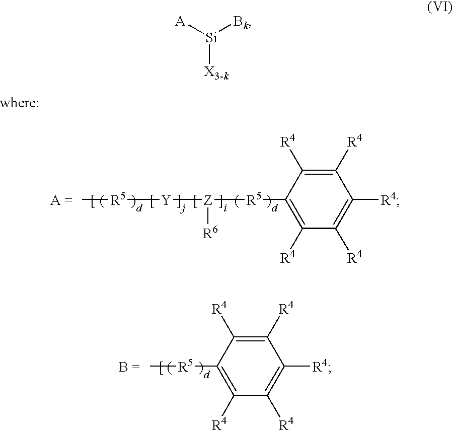
Some preferred silanes for use in the present invention can also be represented by the general formula
Figure US07695890-20100413-C00001

wherein:
    • each of i, j, and k is individually selected from the group consisting of 0 and 1, and if one of i and j is 1, then the other of i and j is 0;
    • each R4 is individually selected from the group consisting of hydrogen, the halogens, C1-C8 (preferably C1-C4) alkyls, C1-(C (preferably C1-C4) alkoxys, C1-C8 (preferably C1-C4) haloalkyls, aminos, and C 1-C8 (preferably C1-C4) alkylaminos;
    • each R5 is individually selected from the group consisting of C1-C8 (preferably C1-C4) aliphatic groups;
    • each R6 is individually selected from the group consisting of hydrogen and haloalkyls (preferably C1-C8, more preferably C1-C4);
    • each X is individually selected from the group consisting of halogens, hydroxyls, C1-C4 alkoxys and C1-C4 carboxyls;
    • Y is selected from the group consisting of oxygen and sulfur;
    • Z is selected from the group consisting of nitrogen and phosphorus; and
    • each d is individually selected from the group consisting of 0 and 1.
An effective primer layer composition according to the invention is a mixture of a diphenyidialkoxysilane (e.g., diphenyldimethoxysilane) and a phenyltrialkoxysilane, (e.g., phenyltrimethoxysilane) or, even more preferably, a mixture of diphenylsilanediol and phenyltrimethoxysilane in a solution of 1 -methoxy-2-propanol or 1-propoxy-2-propanol with from about 5-10% by weight water. A particularly effective primer layer composition for photosensitive layers comprising a poly(styrene-co-acrylonitrile) polymer is an alcohol and water solution containing from about 0.1-1.0% (preferably from about 0.25-0.5%) by weight diphenylsilanediol and from about 0.1-1.0% (preferably from about 0.25-0.5%) by weight of phenyltrimethoxysilane. Upon heating, diphenylsilanediol and phenylsilanetriol (the hydrolysis product of phenyltrimethoxysilane) condense to from siloxane bonds and establish a three-dimensional silicone coating layer on the substrate.
Another preferred silane has the formula
Figure US07695890-20100413-C00002

wherein:
    • each R7 is individually selected from the group consisting of hydrogen, the halogens, C1-C8 (preferably C1-C4) alkyls, C1-C, (preferably C1-C4) alkoxys, C1-C, (preferably C1-C4) haloalkyls, aminos, and C1-C8 (preferably C1-C4) alkylaminos; and
    • each R8 is individually selected from the group consisting of C1-C8 (preferably C1-C4) aliphatic groups.
Silanes having this structure are not only compatible with styrene-containing copolymers, but they are also reactive with ester, benzyl chloride, and/or epoxy groups, and they are excellent adhesion promoters. One particularly preferred silane within the scope of this formula is
Figure US07695890-20100413-C00003

This silane is 3-[N-phenylamino]propyltrimetlioxysilane (mentioned above), and it is commercially available from Lancaster Synthesis and Gelest Corporation.
The silane should be included in the primer layer composition at a level of from about 0.1% to about 3% by weight, preferably from about 0.2% to about 2% by weight, and even more preferably from about 0.5% to about 1% by weight, based upon the total weight of solids in the primer layer composition taken as 100% by weight
The solvent system utilized in the primer layer composition should have a boiling point of from about 100° C. to about 220° C., and preferably from about 140° C. to about 180° C. The solvent system should be utilized at a level of from about 30% to about 99.9% by weight, and preferably from about 40% to about 80% by weight, based upon the total weight of the primer layer composition taken as 100% by weight. Preferred solvent systems include a solvent selected from the group consisting of methanol, ethanol, isopropanol, butanol, 1-methoxy-2-propanol, ethylene glycol monomethyl ether, and 1-propoxy-2-propanol, and mixtures thereof. In one preferred embodiment, water is included in the solvent system at a level of from about 20% to about 60% by weight, and preferably from about 20% to about 40% by weight, based upon the total weight of the primer layer composition taken as 100% by weight.
The primer layer composition can also include a catalyst. Suitable catalysts include any inorganic or organic acid (e.g., hydrochloric acid, sulfuric acid, phosphoric acid, acetic acid) or an inorganic or organic base (e.g., potassium hydroxide, TMAH, ammonia, amines). The catalyst is preferably present in the primer layer composition at levels of from about 0.01% to about 0.5% by weight, more preferably from about 0.1% to about 0.3% by weight, and even more preferably from about 0.02% to about 0.03% by weight, based upon the total weight of solids in the primer layer composition taken as 100% by weight.
Finally, the primer layer can also include a number of optional ingredients, such as a surfactant. In one embodiment, from about 100 ppm to about 150 ppm of a surfactant such as FC4430 (available from 3M) or Triton X-100 (available from 3M) can be added to make a uniform primer coating that is defect-free.
The Photosensitive Layer
The photosensitive layer is formed from a composition comprising a polymer dispersed or dissolved in a solvent system. A preferred polymer is a terpolymer comprising recurring: styrene monomers; acrylonitrile monomers; and monomers comprising functional groups that react with amines.
Preferred styrene monomers have the formula
Figure US07695890-20100413-C00004
Preferred acrylonitrile monomers have the formula
Figure US07695890-20100413-C00005
Preferred monomers comprising functional groups for reacting with amines include monomers comprising one or more epoxy groups (e.g., glycidyl methacrylate, glycidyl acrylate, vinylbenzoyl glycidyl ether). One example is represented by the formula
Figure US07695890-20100413-C00006
In each of the above formulas (I)-(III):
    • each R1 is individually selected from the group consisting of hydrogen and C1-C8 (and preferably C1-C4) alkyls; and
    • each R2 is individually selected from the group consisting of hydrogen, C1-C8 (and preferably C1-C4) alkyls, and C1-C8 (and preferably C1-C4) alkoxys.
The polymer preferably comprises from about 35% to about 75% by weight of monomer (I), more preferably from about 40% to about 70% by weight of monomer (I), and even more preferably from about 50% to about 65% by weight of monomer (I). The polymer preferably comprises from about 20% to about 40% by weight of monomer (II), more preferably from about 25% to about 35% by weight of monomer (II), and even more preferably from about 25% to about 30% by weight of monomer (II). Finally, the polymer preferably comprises from about 5% to about 15% by weight of monomer (III), more preferably from about 6% to about 12% by weight of monomer (III), and even more preferably from about 8% to about 10% by weight of monomer (III). Each of the above percentages by weight is based upon the total weight of the polymer taken as 100% by weight.
It is preferred that the polymer have a weight average molecular weight of from about 10,000 Daltons to about 80,000 Daltons, preferably from about 20,000 Daltons to about 60,000 Daltons, and even more preferably from about 30,000 Daltons to about 50,000 Daltons.
Monomers other than monomers (I), (II), and (III) can also be present in the polymer, if desired. When other monomers are present, the combined weight of monomers (I), (II), and (III) in the polymer is preferably at least about 60% by weight, and more preferably from about 70% to about 90% by weight, based upon the total weight of the polymer taken as 100% by weight. Examples of suitable other monomers include those having functional groups that can react with groups in the primer layer for achieving chemical bonding between the two layers. These monomers may have, by way of example, haloalkyl (e.g., benzyl chloride, 2-chloroethyl methacrylate), ester (methacrylates, acrylates, maleates, fumarates, isocyanates), or anhydride functional groups, which react readily with functional groups such as hydroxyl, amino, or oxiranyl groups that can be present in the primer layer.
The polymer should be included in the photosensitive layer composition at a level of from about 90% to about 98% by weight, and preferably from about 90% to about 95% by weight, based upon the total weight of solids in the photosensitive layer composition taken as 100% by weight.
The photosensitive composition will also comprise a photoacid generator (PAG). The PAG generates a strong acid or superacid when exposed to actinic radiation such as UV light. Examples of suitable PAGs include those selected from the group consisting of triarylsulfonium hexafluoroantimonate, triarylulfonium hexafluorophosphate, diaryliodonium hexafluoroantimonate, diaryliodonium hexafluorophosphate,
Figure US07695890-20100413-C00007

where each R3 is individually selected from the group consisting of C3H7, C8H17, CH3C6H4, and camphor. The PAGs of formulas (IV) and (V) are sold by Ciba Specialty Chemicals as The CGI 13XX Family and The CGI 26X Family, respectively.
The PAG should be included in the photosensitive composition at a level of from about 2% to about 10% by weight, and preferably from about 5% to about 8% by weight, based upon the total weight of solids in the photosensitive composition taken as 100% by weight.
The solvent system utilized in the photosensitive composition should have a boiling point of from about 120° C. to about 200° C., and preferably from about 130° C. to about 180° C. The solvent system should be utilized at a level of from about 70% to about 95% by weight, and preferably from about 80% to about 90% by weight, based upon the total weight of the photosensitive composition taken as 100% by weight. Preferred solvent systems include a solvent selected from the group consisting of methyl isoamyl ketone, di(ethylene glycol) dimethyl ether, propylene glycol monomethyl ether acetate, ethyl lactate, cyclohexanone, and mixtures thereof.
Application Process
Preferred substrates for use in this process include those comprising silicon. Some particularly preferred substrates are selected from the group consisting of Si substrates, SiO2 substrates, Si3N4 substrates, SiO2 on silicon substrates, Si3N4 on silicon substrates, glass substrates, quartz substrates, ceramic substrates, semiconductor substrates, and metal substrates.
The silane and any other components are dissolved in the primer solvent system to form the silane composition. This composition is then spin-applied onto the substrate at about 500-5,000 rpm, and preferably from about 1000-3,000 rpm, for about 30-90 seconds, and preferably for about 60 seconds. It is then baked at a temperature of from about 60-110° C. for about 60-180 seconds (preferably about 120 seconds), and then at about 150-250° C. for about 60-180 seconds (preferably about 120 seconds) in order to condense the silane molecules into a continuous film that is bonded to surface hydroxyl groups present on typical microelectronic substrates. That is, the hydrolyzed silane reacts with the silanol groups present in the silicon-containing substrate and also self-crosslinks by condensation. It is preferred that the primer layer have an average thickness (as measured by an ellipsometer over 5 different points) of less than about 50 nm and more preferably from about 20 nm to about 30 nm.
For the photosensitive layer, the polymer, PAG, and any other components are dissolved in the solvent system and spin coated onto the substrate at about 1,000-5,000 rpm, and preferably from about 1,000-2,000 rpm, for about 30-90 seconds, and preferably about 60 seconds. It is then baked at a temperature of from about 100-120° C. for about 60-180 seconds (preferably about 120 seconds). The polymer solids level and spinning conditions are typically adjusted to achieve an average coating thickness after baking (as measured by an ellipsometer over 5 different points) of from about 500 nm to about 3,000 nm, and preferably from about 1,000 nm to about 2,000 nm, depending upon the degree of coverage required over device topography on the substrate. Advantageously, the epoxy or other reactive group in the photosensitive layer polymer form covalent bonds with an amine or other reactive group on the silane of the primer layer.
The photosensitive layer is then imaged by exposing it to UV light with a wavelength of from about 150-500 nm (e.g., about 248 nm or about 365 nm), preferably in a dose of about 500 mJ/cm2. The coating is then preferably post-exposure baked at about 110° C. to about 30° C. for about 2 minutes, and developed with a solvent for about 1 minute. Finally, the coating is baked at about 200° C. to about 250° C. for about 5 minutes.
Exposure to light causes the PAG to generate an acid, and this acid initiates crosslinking of the polymer (preferably via the epoxy groups) in the photosensitive layer. The crossliniked epoxy groups will have the structure
Figure US07695890-20100413-C00008
The exposed areas become substantially insoluble (e.g., less than about 1% by weight soluble, preferably less than about 0.05% soluble, and more preferably about 0% soluble) in typical solvent developers such as propylene glycol monomethyl ether acetate, methyl isoamyl ketone, and ethyl acetoacetate. The unexposed areas remain soluble in these developers and are thus readily removed during developing. As a result, the pattern can be easily transferred with no additional etching steps to remove the protective layer being needed.
Practicing the present invention will result in a protective layer system that suffers little or no undercutting during etching processes. That is, the layer systems will exhibit less than about 100 μm, preferably less than about 70 μm, and more preferably less than about 50 μm of undercutting when subjected for about 2 hours (or even about 3 hours) to etching in an approximately 30-35% by weight aqueous KOH solution having a temperature of about 83-87° C. Undercutting is determined by measuring the width of overhanging protective layer at the edge of etched areas as observed under a confocal microscope. 5 Furthermore, the inventive protective systems will experience very little or no etchant penetration during etching processes. Thus, when subjected for about 2 hours (or even about 3 hours) to etching in an approximately 30-35% by weight aqueous KOH solution having a temperature of about 83-87 ° C., the inventive protective systems will have less than about 0.1 pinholes per cm2 of substrate, and preferably less than about 0.05 pinholes per cm2 of substrate, when observed under a microscope at 10× magnification. This is different from prior art photosensitive layers, which would dissolve relatively quickly in KOH and thus required the presence of a separate protective layer such as a silicon nitride layer.
EXAMPLES
The following examples set forth preferred methods in accordance with the invention. It is to be understood, however, that these examples are provided by way of illustration and nothing therein should be taken as a limitation upon the overall scope of the invention.
Example 1
1. Terpolymer Synthesis in Cyclopentanone
A solution was made by dissolving 67.50 g of styrene, 25.00 g of acrylonitrile, 7.50 g of glycidyl methacrylate, and 1.25 g of 2,2′-azobisisobutyronitrile in 400 g of cyclopentanone, all of which were obtained from Aldrich. The solution was heated to 65° C. under nitrogen while undergoing magnetic stirring. The polymerization was allowed to proceed at 65° C. for 98 hours. The actual yield was determined by solids analysis to be 97% of the theoretical yield.
2. Topcoat Solution Formulation
In this preparation procedure, 25.01 g of propylene glycol methyl ether acetate (PGMEA, General Chemical) and 1.03 g of UVI-6976 (a triarylsulfonium hexafluoroantimonate; a photoacid generator obtained from Dow Chemical) were added to 50.03 g of the terpolymer solution synthesized in Part 1 of this Example. The resulting solution was filtered through a 0.1-μm membrane filter.
3. Primer Solution Formulation
To make a primer solution, 1.02 g of N-phenylaminopropyltrimethoxysilane (obtained from Gelest) were dissolved in a mixture of 120.4 g of propylene glycol propyl ether (obtained from General Chemical) and 80.2 g of deionized water. The solution was filtered through a 0.1-μm membrane filter.
4. Preparation and Patterning of Negative Photoresist Coating
The primer solution in Part 3 of this Example was spin coated onto a silicon wafer at 1,500 rpm for 1 minute. The primer coating was baked at 75° C. for 2 minutes and then at 180° C. for 2 minutes. The topcoat solution of Part 2 of this Example was then spin coated over the primer layer at 1,500 rpm for 1 minute. The topcoat was baked at 100° C. for 2 minutes. The coating was imaged by exposing it to UV light at 2)0 a wavelength of 365 nm in a dose of 500 mJ/cm2, baking at 130° C. for 2 minutes, and developing with acetone for 1 minute. Finally, the combination was baked at 230° C. for 5 minutes. A negative pattern was obtained.
5. Etching of Silicon Wafer
The wafer prepared and patterned in Part 4 of this Example was etched in 30% KOH aqueous solution at 85° C. for 1 hour. The silicon was etched 70 μm deep in areas without the polymer coating. The polymer-coated areas remained intact. The pattern was transferred to the silicon wafer in essentially the same manner as is the case with prior art silicon nitride masking methods.
Example 2
1. Terpolymer Synthesis in PGMEA
A solution was made by dissolving 27.07 g of styrene, 10.00 g of acrylonitrile, 3.08 g of glycidyl methacrylate, and 0.51 g of dicumyl peroxide (obtained from Aldrich) in 160 g of PGMEA. The solution was heated to 120° C. under nitrogen while undergoing magnetic stirring. The polymerization was allowed to proceed at 120° C. for 24 hours. The actual yield was determined by solids analysis to be 95.5% of the theoretical yield.
2. Topcoat Solution Formulation
In this preparation procedure, 4.54 g of PGMEA and 0.114 g of UVI-6976 were added to 5.03 g of the terpolymer solution synthesized in Part 1 of this Example. The solution was filtered through a 0.1 μm membrane filter.
3. Preparation and Patterning of Negative Photoresist Coating
The primer solution of Part 2 of Example 1 was spin coated onto a silicon wafer at 1,500 rpm for 1 minute. The primer coating was baked at 60° C. for 5 minutes and at 180° C. for 2 minutes. The topcoat solution from Part 2 of this Example was then spin coated onto the wafer at 1,500 rpm for 1 minute. The topcoat was baked at 100° C. for 2 minutes. After the coating was imaged by exposing it to UV light at 254 nm in a dose of 500 mJ/cm2, it was baked at 130° C. for 2 minutes and then developed with PGMEA for 1 minute. The coating was finally baked at 230 ° C. for 5 minutes. A negative pattern was obtained.
4. Etching of Silicon Wafer
The wafer prepared and patterned in Part 3 of this Example was etched in 30% KOH aqueous solution at 80° C. for 1 hour. The silicon was etched 58 μm deep in the areas without the polymer coating. The polymer-coated areas remained intact The pattern was transferred to the silicon wafer in essentially the same way as with prior art silicon nitride masking methods.
Example 3
1. Terpolymer Synthesis in PGMEA
A solution was made by dissolving 168.0 g of styrene, 84.0 g of acrylonitrile, 28.3 g of glycidyl methacrylate, and 7.0 g of dicumyl peroxide in 1,120 g of PGMEA. The solution was heated to 120° C. under nitrogen while undergoing magnetic stirring. The polymerization was allowed to proceed at 120° C. for 28 hours. The actual yield was found by solid analysis to be 97.5% of the theoretical. The terpolymer was precipitated in isopropanol, filtered, and dried overnight under vacuum at 50° C.
2. Topcoat Solution Formulation
In this preparation procedure, 32.8 g of the terpolymer synthesized in Part 1 of this Example were dissolved in 140.0 g of PGMEA and 40.0 g of ethyl acetylacetate. Next, 6.0 g of UVI-6976 were added, and the solution was filtered through a 0.1-μm membrane filter.
3. Primer Solution Formulation
To prepare a primer solution, 2,04 g of N-phenylaminopropyltrimethoxysilane were dissolved in a mixture of 77.50 g of propylene glycol propyl ether (PnP), 120.14 g of deionized water, 0.51 g of acetic acid, and 0.03 g of FC4430 (a surfactant). The solution was stirred magnetically for more than 2 hours. It was filtered through a 0.1-μm membrane filter.
4. Preparation and Patterning of Negative Photoresist Coating
The primer solution prepared in Part 3 of this Example was spin coated onto a silicon wafer at 1,500 rpm for 1 minute. The primer coating was baked at 100° C. for 1 minute and then at 205 ° C. for 1 minute. The topcoat solution from Part 2 of this Example was spin coated over the primer layer at 1,500 rpm for I minute. The topcoat was baked at 110° C. for 2 minutes. The coating was imaged by exposing it to UV light at a wavelength of 365 nm in a dose of 500 mJ/cm2, baking at 130 ° C. for 2 minutes, and developing with PGMEA for 1 minute. Finally, the combination was baked at 230° C. for 5 minutes. A negative pattern was obtained.
5. Etching of Silicon Wafer
The wafer prepared and patterned in Part 4 of this Example was etched in 30% KOH aqueous solution at 75° C. for 4 hours. The silicon was etched 178 μm deep in the areas without the polymer coating. The polymer-coated area remained intact. The pattern was transferred to the silicon wafer in essentially the same manner as prior art silicon nitride masking methods.

Claims (36)

1. A photosensitive composition useful as a protective layer, said composition being alkaline-resistant and negative-acting and said composition comprising a polymer and a photoacid generator dissolved or dispersed in a solvent system, said polymer comprising:
Figure US07695890-20100413-C00009
(III) a monomer comprising at least one epoxy group,
wherein in (I) and (II):
each R1 is individually selected from the group consisting of hydrogen and C1-C8 alkyls; and
each R2 is individually selected from the group consisting of hydrogen, and C1-C8 alkyls, wherein said first polymer comprises from about 35% to about 75% by weight of (I) and from about 20% to about 40% by weight of (II).
2. The composition of claim 1, wherein said monomer (III) is selected from the group consisting of glycidyl methacrylate, glycidyl acrylate, and vinylbenzyl glycidyl ether monomers.
3. The composition of claim 1, wherein said monomer (III) has the formula
Figure US07695890-20100413-C00010
wherein each R1 is individually selected from the group consisting of hydrogen and C1-C8 alkyls.
4. The composition of claim 1, wherein said photoacid generator is selected from the group consisting of triarylsulfonium hexafluoroantimonate, triarylsulfonium hexafluoro-phosphate, diaryliodonium hexafluoroantimonate, diaryliodonium hexafluorophosphate,
Figure US07695890-20100413-C00011
wherein each R3 is individually selected from the group consisting of C3H7, C8H17, CH3C6H4, and camphor.
5. The composition of claim 1, wherein said polymer comprises from about 35% to about 75% by weight of (I), from about 20% to about 40% by weight of(II), and from about 5% to about 15% by weight of (III), based upon the total weight of the polymer taken as 100% by weight.
6. A method of forming a microelectronic structure, said method comprising:
providing a microelectronic substrate;
applying a primer layer to said substrate, said primer layer comprising a silane dispersed or dissolved in a solvent system;
applying a photosensitive layer to said primer layer, said photosensitive layer comprising a photoacid generator and a polymer dispersed or dissolved in a solvent system, said
polymer comprising:
Figure US07695890-20100413-C00012
(III) a monomer comprising at least one epoxy group,
wherein in (I) and (II):
each R1 is individually selected from the group consisting of hydrogen and C1-C8 alkyls; and
each R2 is individually selected from the group consisting of hydrogen, and C1-C8 alkyls; and
etching said stack with KOH so as to transfer the pattern of said photosensitive layer to said substrate, wherein said photosensitive layer exhibits less than about 0.1 pinholes per cm2 of substrate.
7. The method of claim 6, wherein said monomer (III) is selected from the group consisting of glycidyl methacrylate, glycidyl acrylate, and vinylbenzyl glycidyl ether monomers.
8. The method of claim 6, wherein said monomer (III) has the formula
Figure US07695890-20100413-C00013
wherein each R1 is individually selected from the group consisting of hydrogen and C1-C8 alkyls.
9. The method of claim 6, wherein said photoacid generator is selected from the group consisting of triarylsulfonium hexafluoroantimonate, triarylsulfonium hexafluorophosphate, diaryliodonium hexafluoroantimonate, diaryliodonium hexafluorophosphate,
Figure US07695890-20100413-C00014
wherein each R3 is individually selected from the group consisting of C3H7, C8H17, CH3C6H4, and camphor.
10. The method of claim 6, wherein said polymer comprises from about 35% to about 75% by weight of (I), from about 20% to about 40% by weight of(II), and from about 5% to about 15% by weight of (III), based upon the total weight of the polymer taken as 100% by weight.
11. The method of claim 6, wherein said silane having a formula selected from the group consisting of
Figure US07695890-20100413-C00015
wherein:
each of i, j, and k is individually selected from the group consisting of 0 and 1, and if one of i and j is 1, then the other of i and j is 0;
each R4 is individually selected from the group consisting of hydrogen, the halogens, C1-C8 alkyls, C1-C8 alkoxys, C1-C8 haloalkyls, aminos, and C1-C8 alkylaminos;
each R5 is individually selected from the group consisting of C1-C8 aliphatic groups;
each R6 is individually selected from the group consisting of hydrogen and haloalkyls;
each X is individually selected from the group consisting of halogens, hydroxyls, C1-C4 alkoxys and C1-C4 carboxyls;
Y is selected from the group consisting of oxygen and sulfur;
Z is selected from the group consisting of nitrogen and phosphorus; and each d is individually selected from the group consisting of 0 and 1; and
Figure US07695890-20100413-C00016
wherein:
each R7 is individually selected from the group consisting of hydrogen, the halogens, C1-C8 alkyls, C1-C8 alkoxys, C1-C8 haloalkyls, aminos, and C1-C8 alkylaminos; and
each R8 is individually selected from the group consisting of C1-C8 aliphatic groups.
12. The method of claim 6, said silane being selected from the group consisting of aminoalkoxysilanes, phenylsilanes, and diphenylsilanes.
13. The method of claim 12, wherein said silane is selected from the group consisting of aminoalkylalkoxysilanes and phenylaminoalkylalkoxysilanes.
14. The method of claim 12, wherein said silane is selected from the group consisting of aminopropyltrimethoxysilane, aminopropyltriethoxysilane, N-phenylaminopropyltrimethoxysilane, N-phenylaminopropyltriethoxysilane, 3-glycidoxypropyltrimethoxysilane, 2-(3,4-epoxycyclohexyl)ethyltrimethoxysilane, 3-mercaptopropyl-trimethoxysilane, phenyltrimethoxysilane, phenyltrichiorosilane, phenyhriethoxysilane, phenyltriacetoxysilane, diphenyldimethoxysilane, diphenyldichiorosilane, diphenylsilanediol 2-phenylethyltrialkoxysilane, p/m-chlorophenyltrimethoxysilane, p/m-bromophenyltrimethoxysilane,(p/m-chloromethyl)phenyltrimethoxysilane, 2-(p/m-methoxy)phenylethyltrimethoxysilane, 2-(p/m-chloromethyl)phenylethyltrimethoxysilane, 3,4-dichiorophenyltrichiorosilane, 3-phenoxypropyltrichlorosilane, 3-(N-phenylamino)propyltrimethoxysilane, and 2-(diphenylphosphino)ethyltriethoxysilane.
15. The method of claim 6, further comprising baking said primer layer after said primer layer applying.
16. The method of claim 15, wherein said primer layer further comprises a catalyst, and said primer layer baking results in crosslinking of said silane.
17. The method of claim 6, further comprising baking said photosensitive layer after said photosensitive layer applying.
18. The method of claim 17, wherein said baking causes the polymer of said photosensitive layer to covalently bond with the silane of said primer layer.
19. The method of claim 6, further comprising exposing a first portion of said photosensitive layer to actinic radiation while a second portion of said photosensitive layer is not exposed to actinic radiation.
20. The method of claim 19, wherein said first portion of said photosensitive layer crosslinks during said exposing.
21. The method of claim 20, further comprising baking said photosensitive layer after said exposing to actinic radiation.
22. The method of claim 20, further comprising developing said photosensitive layer.
23. The method of claim 22, wherein said developing results in the second portion of said photosensitive layer being substantially removed during said developing step so as to form a stack including a photosensitive layer having a pattern formed therein.
24. The method of claim 23, further comprising baking said photosensitive layer after said developing.
25. The method of claim 6, wherein said photosensitive layer exhibits less than about 100 μm of undercutting during etching.
26. The method of claim 6, wherein said substrate is selected from the group consisting of Si substrates, SiO2 substrates, Si3N4 substrates, SiO2 on silicon substrates, Si3N4 on silicon substrates, glass substrates, quartz substrates, ceramic substrates, semi conductor substrates, and metal substrates.
27. A microelectronic structure comprising:
a microelectronic substrate;
a primer layer adjacent said substrate, said primer layer comprising a crosslinked silane; a photosensitive layer adjacent said primer layer, said photosensitive layer being alkaline-resistant and comprising a polymer comprising:
Figure US07695890-20100413-C00017
(III) a monomer comprising at least one crosslinked epoxy group,
wherein in (I) and (II):
each R1 is individually selected from the group consisting of hydrogen and C1-C8 alkyls; and
each R2 is individually selected from the group consisting of hydrogen, and C1-C8 alkyls, wherein said first polymer comprises from about 35% to about 75% by weight of (I) and from about 20% to about 40% by weight of (II).
28. The microelectronic structure of claim 27, wherein said crosslinked epoxy group comprises
Figure US07695890-20100413-C00018
29. The microelectronic structure of claim 27, wherein said silane comprises an amine, and the polymer of said photosensitive layer comprises an epoxy group covalently bonded with said amine.
30. The microelectronic structure of claim 27, wherein said polymer comprises from about 35% to about 75% by weight of (I), from about 20% to about 40% by weight of (II), and from about 5% to about 15% by weight of (III), based upon the total weight of the polymer taken as 100% by weight.
31. The microelectronic structure of claim 27, said silane having a formula selected from the group consisting of
Figure US07695890-20100413-C00019
wherein:
each of i, j, and k is individually selected from the group consisting of 0 and 1, and if one of i and j is 1, then the other of i and j is 0;
each R4 is individually selected from the group consisting of hydrogen, to halogens, C1-C8 alkyls, C1-C8 alkoxys, C1-C8 haloalkyls, aminos, and C1-C8 alkylaminos;
each R5 is individually selected from to group consisting of C1-C8 aliphatic groups;
each R6 is individually selected from to group consisting of hydrogen and haloalkyls;
each X is individually selected from the group consisting of halogens, hydroxyls, C1-C4 alkoxys and C1-C4 carboxyls;
Y is selected from the group consisting of oxygen and sulfur;
Z is selected from the group consisting of nitrogen and phosphorus; and
each d is individually selected from the group consisting of 0 and 1; and
Figure US07695890-20100413-C00020
wherein:
each R7 is individually selected from the group consisting of hydrogen, the halogens, C1-C8 alkyls, C1-C8 alkoxys, C1-C8, haloalkyls, aminos, and C1-C8 alkylaminos; and
each R8 is individually selected from the group consisting of C1-C8 aliphatic groups.
32. The microelectronic structure of claim 27, said silane being selected from the group consisting of aminoalkoxysilanes, phenylsilanes, and diphenylsilanes.
33. The microelectronic structure of claim 32, wherein said silane is selected from the group consisting of aminoalkylalkoxysilane and phenylaminoalkylalkoxysilanes.
34. The microelectronic structure of claim 32, wherein said silane is selected from the group consisting of aminopropyltrimethoxysilane, aminopropyltriethoxysilane, N-phenylaminopropyltrimethoxysilane, N-phenylaminopropyltriethoxysilane, 3-glycidoxypropyltrimethoxysilane, 2-(3,4-epoxycyclohexyl)ethyltrimethoxysilane, 3-mercaptopropyl-trimethoxysilane, phenyltrimethoxysilane, phenyltrichiorosilane, phenyltriethoxysilane, phenyltriacetoxysilane, diphenyldimethoxysilane, diphenyldichiorosilane, diphenylsilanediol 2-phenylethyltrialkoxysilane, p/m-chlorophenyltrimethoxysilane, p/m-bromophenyltrimethoxysilane,(p/m-chloromethyl)phenyltrimethoxysilane, 2-(p/m-methoxy)phenyl ethyltrimethoxysilane, 2-(p/m-chloromethyl)phenylethyltrimethoxysilane, 3,4-dichlorophenyltrichlorosilane, 3-phenoxypropyltrichiorosilane, 3-(N-phenylamino)propyltrimethoxysilane, and 2-(diphenylphosphino)ethyltriethoxysilane.
35. The microelectronic structure of claim 27, wherein said substrate is selected from the group consisting of Si substrates, SiO2 substrates, Si3N4 substrates, SiO2 on silicon substrates, Si3N4 on silicon substrates, glass substrates, quartz substrates, ceramic substrates, semiconductor substrates, and metal substrates.
36. A method of forming a microelectronic structure, said method comprising:
providing a microelectronic substrate selected from the group consisting of Si substrates, SiO2 substrates, Si3N4 substrates, SiO2 on silicon substrates, Si3N4 on silicon substrates, glass substrates, quartz substrates, ceramic substrates, semiconductor substrates, and metal substrates;
applying a primer layer to said substrate, said primer layer comprising a silane dispersed or dissolved in a solvent system;
applying a photosensitive layer to said primer layer, said photosensitive layer comprising a photoacid generator and a polymer dispersed or dissolved in a solvent system, said polymer comprising:
Figure US07695890-20100413-C00021
(III) a monomer comprising at least one epoxy group,
wherein in (I) and (II):
each R1 is individually selected from the group consisting of hydrogen and C1-C8 alkyls; and
each R2 is individually selected from the group consisting of hydrogen, and C1-C8 alkyls.
US11/470,520 2005-09-09 2006-09-06 Negative photoresist for silicon KOH etch without silicon nitride Active 2027-03-29 US7695890B2 (en)

Priority Applications (7)

Application Number Priority Date Filing Date Title
US11/470,520 US7695890B2 (en) 2005-09-09 2006-09-06 Negative photoresist for silicon KOH etch without silicon nitride
CN200680032665.4A CN101258444B (en) 2005-09-09 2006-09-07 Negative photoresist for silicon KOH etch without silicon nitride
JP2008530189A JP4870769B2 (en) 2005-09-09 2006-09-07 Negative photoresist for silicon KOH etching without using silicon nitride
PCT/US2006/034817 WO2007030593A1 (en) 2005-09-09 2006-09-07 Negative photoresist for silicon koh etch without silicon nitride
KR1020087007155A KR101360503B1 (en) 2005-09-09 2006-09-07 Negative photoresist for silicon koh etch without silicon nitride
EP06803089A EP1932060B1 (en) 2005-09-09 2006-09-07 Negative photosensitive composition for silicon koh etch without using silicon nitride hardmask
TW095133184A TWI411879B (en) 2005-09-09 2006-09-08 Negative photoresist for silicon koh etch without silicon nitride

Applications Claiming Priority (2)

Application Number Priority Date Filing Date Title
US71596405P 2005-09-09 2005-09-09
US11/470,520 US7695890B2 (en) 2005-09-09 2006-09-06 Negative photoresist for silicon KOH etch without silicon nitride

Publications (2)

Publication Number Publication Date
US20070075309A1 US20070075309A1 (en) 2007-04-05
US7695890B2 true US7695890B2 (en) 2010-04-13

Family

ID=37836158

Family Applications (1)

Application Number Title Priority Date Filing Date
US11/470,520 Active 2027-03-29 US7695890B2 (en) 2005-09-09 2006-09-06 Negative photoresist for silicon KOH etch without silicon nitride

Country Status (7)

Country Link
US (1) US7695890B2 (en)
EP (1) EP1932060B1 (en)
JP (1) JP4870769B2 (en)
KR (1) KR101360503B1 (en)
CN (1) CN101258444B (en)
TW (1) TWI411879B (en)
WO (1) WO2007030593A1 (en)

Cited By (2)

* Cited by examiner, † Cited by third party
Publication number Priority date Publication date Assignee Title
US20150279666A1 (en) * 2012-10-12 2015-10-01 John Cleaon Moore Compositions and methods of rinsable primers used to aid in the removal of temporary functional coatings
US9299778B2 (en) 2012-11-08 2016-03-29 Brewer Science Inc. CVD-free, scalable processes for the production of silicon micro- and nanostructures

Families Citing this family (12)

* Cited by examiner, † Cited by third party
Publication number Priority date Publication date Assignee Title
US7316844B2 (en) * 2004-01-16 2008-01-08 Brewer Science Inc. Spin-on protective coatings for wet-etch processing of microelectronic substrates
US7695890B2 (en) 2005-09-09 2010-04-13 Brewer Science Inc. Negative photoresist for silicon KOH etch without silicon nitride
US7709178B2 (en) * 2007-04-17 2010-05-04 Brewer Science Inc. Alkaline-resistant negative photoresist for silicon wet-etch without silicon nitride
US8192642B2 (en) 2007-09-13 2012-06-05 Brewer Science Inc. Spin-on protective coatings for wet-etch processing of microelectronic substrates
SG179209A1 (en) * 2009-09-16 2012-05-30 Brewer Science Inc Scratch-resistant coatings for protecting front-side circuitry during backside processing
KR101384457B1 (en) * 2011-08-04 2014-04-14 주식회사 엘지화학 Silane-based compounds and photosensitive resin composition comprising the same
US9000556B2 (en) * 2011-10-07 2015-04-07 International Business Machines Corporation Lateral etch stop for NEMS release etch for high density NEMS/CMOS monolithic integration
JP6088813B2 (en) * 2012-12-14 2017-03-01 東京応化工業株式会社 Crude resin purification method, resist resin production method, resist composition production method, and resist pattern formation method
TWI597574B (en) * 2015-08-19 2017-09-01 奇美實業股份有限公司 Photosensitive resin composition and application thereof
CN110908240A (en) * 2018-09-14 2020-03-24 江西省长益光电有限公司 Photoresist for chip and photoetching process
KR102031251B1 (en) * 2019-03-06 2019-10-11 영창케미칼 주식회사 Composition for etching a silicone nitride layer and etching method using the same
JP7222811B2 (en) 2019-06-04 2023-02-15 キオクシア株式会社 IMPRINT APPARATUS, IMPRINT METHOD, AND SEMICONDUCTOR DEVICE MANUFACTURING METHOD

Citations (37)

* Cited by examiner, † Cited by third party
Publication number Priority date Publication date Assignee Title
US3398044A (en) 1965-02-01 1968-08-20 Dow Corning Bonding of organic resins or rubbers to inorganic substances
US3461027A (en) 1966-02-01 1969-08-12 Dow Corning Bonding of thermoplastic polymer resins to silane-primed siliceous or metallic materials
US3468834A (en) 1965-02-15 1969-09-23 Akira Oda Coating compositions and process of preparing the same
US3585103A (en) 1968-09-23 1971-06-15 Hercules Inc Priming composition comprising a coupling agent and a polyfunctional azide for bonding polymers to glass,metal and metal oxide substrates
US3826709A (en) 1969-09-02 1974-07-30 Bethlehem Steel Corp Process for laminating phosphate coated steel with abs resin
US4800125A (en) 1986-10-07 1989-01-24 Dow Corning Corporation Coupling agent compositions
US4826564A (en) 1987-10-30 1989-05-02 International Business Machines Corporation Method of selective reactive ion etching of substrates
US5077174A (en) * 1990-04-10 1991-12-31 E. I. Du Pont De Nemours And Company Positive working dry film element having a layer of resist composition
US5100503A (en) * 1990-09-14 1992-03-31 Ncr Corporation Silica-based anti-reflective planarizing layer
EP0539973A2 (en) 1991-11-01 1993-05-05 The Furukawa Electric Co., Ltd. A surface-protection method during etching
US5217568A (en) 1992-02-03 1993-06-08 Motorola, Inc. Silicon etching process using polymeric mask, for example, to form V-groove for an optical fiber coupling
US5353705A (en) 1992-07-20 1994-10-11 Presstek, Inc. Lithographic printing members having secondary ablation layers for use with laser-discharge imaging apparatus
US5585450A (en) 1991-12-10 1996-12-17 The Dow Chemical Company Oligomerized cyclobutarene resins
US5753523A (en) 1994-11-21 1998-05-19 Brewer Science, Inc. Method for making airbridge from ion-implanted conductive polymers
US5874365A (en) 1993-11-04 1999-02-23 Nippondenso Co., Ltd. Semiconductor wafer etching method
US5922410A (en) 1995-01-18 1999-07-13 Rohm And Haas Company Wood coating composition
US6162860A (en) * 1997-11-12 2000-12-19 S. C. Johnson Commercial Markets, Inc. Solvent based interactive polymeric compositions containing a substantially non-gelled composition
US6358665B1 (en) 1998-08-07 2002-03-19 Clariant International Ltd. Radiation-sensitive composition of chemical amplification type
US20020051928A1 (en) 2000-09-11 2002-05-02 Shipley Company, L.L.C. Photoresist composition
US20020058749A1 (en) 2000-09-28 2002-05-16 Larson Gary Robert Binder compositions for direct-to-metal coatings
WO2002087340A1 (en) 2001-04-30 2002-11-07 Ak Properties, Inc. Antimicrobial coated metal sheet
US20030216508A1 (en) * 2002-05-14 2003-11-20 Lee Coreen Y. Polycarbonate and acrylonitrile-butadiene-styrene polymeric blends with improved impact resistance
US6773867B2 (en) * 1999-09-02 2004-08-10 Fujitsu Limited Negative resist composition, method for the formation of resist patterns and process for the production of electronic devices
US6773862B2 (en) * 2001-10-19 2004-08-10 Fuji Photo Film Co., Ltd. Negative resist composition
JP2004264623A (en) 2003-03-03 2004-09-24 Jsr Corp Radiation-sensitive resin composition, interlayer insulating film, microlens and method for forming these
JP2005008847A (en) 2003-05-28 2005-01-13 Jsr Corp Hardenable resin composition, protective film and method of forming protective film
US20050037281A1 (en) 2003-08-15 2005-02-17 Fuji Photo Film Co., Ltd. Light-sensitive sheet comprising support, first and second light-sensitive layers and barrier layer
US6878502B2 (en) 2001-07-03 2005-04-12 Fuji Photo Film Co., Ltd. Positive resist composition
WO2005052688A2 (en) 2003-11-25 2005-06-09 Tokyo Ohka Kogyo Co., Ltd. Chemically amplified positive photosensitive thermosetting resin composition method of forming cured article and method of producing functional device
US20050158538A1 (en) 2004-01-16 2005-07-21 Brewer Science Inc. Spin-on protective coatings for wet-etch processing of microelectronic substrates
US6956268B2 (en) 2001-05-18 2005-10-18 Reveo, Inc. MEMS and method of manufacturing MEMS
US20060070441A1 (en) 2004-07-12 2006-04-06 Stmicroelectronics S.R.I. Micro-electro-mechanical structure having electrically insulated regions and manufacturing process thereof
WO2006046687A1 (en) 2004-10-29 2006-05-04 Jsr Corporation Positive photosensitive insulating resin composition and cured product thereof
US7049164B2 (en) 2001-09-13 2006-05-23 Silicon Light Machines Corporation Microelectronic mechanical system and methods
US20060166403A1 (en) 2003-02-07 2006-07-27 Dalsa Semiconductor Inc. Fabrication of advanced silicon-based MEMS devices
US20060166393A1 (en) 2005-01-24 2006-07-27 Samsung Electronics Co., Ltd. Manufacturing method of a MEMS structure, a cantilever-type MEMS structure, and a sealed fluidic channel
WO2007030593A1 (en) 2005-09-09 2007-03-15 Brewer Science Inc. Negative photoresist for silicon koh etch without silicon nitride

Family Cites Families (3)

* Cited by examiner, † Cited by third party
Publication number Priority date Publication date Assignee Title
GB2273366B (en) * 1992-11-18 1996-03-27 Du Pont Forming images on radiation-sensitive plates
JPH07261390A (en) * 1994-03-22 1995-10-13 Nippon Oil & Fats Co Ltd Photosetting resin composition
SG98433A1 (en) * 1999-12-21 2003-09-19 Ciba Sc Holding Ag Iodonium salts as latent acid donors

Patent Citations (39)

* Cited by examiner, † Cited by third party
Publication number Priority date Publication date Assignee Title
US3398044A (en) 1965-02-01 1968-08-20 Dow Corning Bonding of organic resins or rubbers to inorganic substances
US3468834A (en) 1965-02-15 1969-09-23 Akira Oda Coating compositions and process of preparing the same
US3461027A (en) 1966-02-01 1969-08-12 Dow Corning Bonding of thermoplastic polymer resins to silane-primed siliceous or metallic materials
US3585103A (en) 1968-09-23 1971-06-15 Hercules Inc Priming composition comprising a coupling agent and a polyfunctional azide for bonding polymers to glass,metal and metal oxide substrates
US3826709A (en) 1969-09-02 1974-07-30 Bethlehem Steel Corp Process for laminating phosphate coated steel with abs resin
US4800125A (en) 1986-10-07 1989-01-24 Dow Corning Corporation Coupling agent compositions
US4826564A (en) 1987-10-30 1989-05-02 International Business Machines Corporation Method of selective reactive ion etching of substrates
US5077174A (en) * 1990-04-10 1991-12-31 E. I. Du Pont De Nemours And Company Positive working dry film element having a layer of resist composition
US5100503A (en) * 1990-09-14 1992-03-31 Ncr Corporation Silica-based anti-reflective planarizing layer
EP0539973A2 (en) 1991-11-01 1993-05-05 The Furukawa Electric Co., Ltd. A surface-protection method during etching
US5585450A (en) 1991-12-10 1996-12-17 The Dow Chemical Company Oligomerized cyclobutarene resins
US5217568A (en) 1992-02-03 1993-06-08 Motorola, Inc. Silicon etching process using polymeric mask, for example, to form V-groove for an optical fiber coupling
US5353705A (en) 1992-07-20 1994-10-11 Presstek, Inc. Lithographic printing members having secondary ablation layers for use with laser-discharge imaging apparatus
US5874365A (en) 1993-11-04 1999-02-23 Nippondenso Co., Ltd. Semiconductor wafer etching method
US5753523A (en) 1994-11-21 1998-05-19 Brewer Science, Inc. Method for making airbridge from ion-implanted conductive polymers
US5922410A (en) 1995-01-18 1999-07-13 Rohm And Haas Company Wood coating composition
US6162860A (en) * 1997-11-12 2000-12-19 S. C. Johnson Commercial Markets, Inc. Solvent based interactive polymeric compositions containing a substantially non-gelled composition
US6358665B1 (en) 1998-08-07 2002-03-19 Clariant International Ltd. Radiation-sensitive composition of chemical amplification type
US6773867B2 (en) * 1999-09-02 2004-08-10 Fujitsu Limited Negative resist composition, method for the formation of resist patterns and process for the production of electronic devices
US20020051928A1 (en) 2000-09-11 2002-05-02 Shipley Company, L.L.C. Photoresist composition
US20020058749A1 (en) 2000-09-28 2002-05-16 Larson Gary Robert Binder compositions for direct-to-metal coatings
US20020185199A1 (en) 2001-04-30 2002-12-12 Myers Frederick A. Antimicrobial coated metal sheet
WO2002087340A1 (en) 2001-04-30 2002-11-07 Ak Properties, Inc. Antimicrobial coated metal sheet
US6956268B2 (en) 2001-05-18 2005-10-18 Reveo, Inc. MEMS and method of manufacturing MEMS
US6878502B2 (en) 2001-07-03 2005-04-12 Fuji Photo Film Co., Ltd. Positive resist composition
US7049164B2 (en) 2001-09-13 2006-05-23 Silicon Light Machines Corporation Microelectronic mechanical system and methods
US6773862B2 (en) * 2001-10-19 2004-08-10 Fuji Photo Film Co., Ltd. Negative resist composition
US20030216508A1 (en) * 2002-05-14 2003-11-20 Lee Coreen Y. Polycarbonate and acrylonitrile-butadiene-styrene polymeric blends with improved impact resistance
US20060166403A1 (en) 2003-02-07 2006-07-27 Dalsa Semiconductor Inc. Fabrication of advanced silicon-based MEMS devices
JP2004264623A (en) 2003-03-03 2004-09-24 Jsr Corp Radiation-sensitive resin composition, interlayer insulating film, microlens and method for forming these
JP2005008847A (en) 2003-05-28 2005-01-13 Jsr Corp Hardenable resin composition, protective film and method of forming protective film
US20050037281A1 (en) 2003-08-15 2005-02-17 Fuji Photo Film Co., Ltd. Light-sensitive sheet comprising support, first and second light-sensitive layers and barrier layer
WO2005052688A2 (en) 2003-11-25 2005-06-09 Tokyo Ohka Kogyo Co., Ltd. Chemically amplified positive photosensitive thermosetting resin composition method of forming cured article and method of producing functional device
US20050158538A1 (en) 2004-01-16 2005-07-21 Brewer Science Inc. Spin-on protective coatings for wet-etch processing of microelectronic substrates
US7316844B2 (en) * 2004-01-16 2008-01-08 Brewer Science Inc. Spin-on protective coatings for wet-etch processing of microelectronic substrates
US20060070441A1 (en) 2004-07-12 2006-04-06 Stmicroelectronics S.R.I. Micro-electro-mechanical structure having electrically insulated regions and manufacturing process thereof
WO2006046687A1 (en) 2004-10-29 2006-05-04 Jsr Corporation Positive photosensitive insulating resin composition and cured product thereof
US20060166393A1 (en) 2005-01-24 2006-07-27 Samsung Electronics Co., Ltd. Manufacturing method of a MEMS structure, a cantilever-type MEMS structure, and a sealed fluidic channel
WO2007030593A1 (en) 2005-09-09 2007-03-15 Brewer Science Inc. Negative photoresist for silicon koh etch without silicon nitride

Non-Patent Citations (15)

* Cited by examiner, † Cited by third party
Title
Bishop, David, Heuer Arthur, and Williams, David, "Microelectromechanical Systems: Technology and Applications," MRS Bulletin, Apr. 2001, pp. 282-288.
Black C. T. et al, "Integration of Self-Assembled Diblock Copolymers for Semiconductor Capacitor Fabrication," Applied Physics Letters, vol. 79, No. 3, Jul. 16, 2001, 2001 American Institute of Physics, pp. 409-411.
Bodas, Dhananjay et al., "PMMA as an etch mask for silicon micromachining-a feasibility study," J. Indian Inst. Sci., vol. 81, Dec. 2001, pp. 645-651.
Brar, A.S., and Pradhan, D.R., "Investigation of Microstructure of the Acrylonitrile-Styrene-Glycidyl Methacrylate Terpolymers by 1D and 2D NMR Spectroscopy," Journal of Applied Polymer Science, vol. 89, 1779-1790 (2003), 2003 Wiley Periodicals, Inc.
Ciba Specialty Chemicals Inc., Photoacid Generators for Microlithography, Jan. 2003, printed in Switzerland.
Elders, Job et al., "Microsystems Technology (MST) and MEMS Applications: An Overview," MRS Bulletin, Apr. 2001, pp. 312-315.
Goldman, Ken et al., "Evaluating the use of hard-mask films during bulk silicon etching," MICRO Magazine, Mar. 1997, p. 67, http://www.mIcromagazine.com/archive/97/03/goldman.html, 7 pages.
Kovacs, Gregory T.A. et al., "Bulk Micromachining of Silicon," Proceedings of the IEEE, vol. 86, No. 8, Aug. 1998, pp. 1536-1551.
Maluf, Nadim, An Introduction to Microelectromechanical Systems Engineering, Norwood, MA: Artech House, Inc., 2000, pp. 54-63.
Office Action in U.S. Appl. No. 11/736,429 dated Jun. 27, 2008, 13 pages.
Robbins, H. and Schwartz, B., "Chemical Etching of Silicon: II. The System HF, HNO3, H2O, and HC2H3O2," Journal of the Electrochemical Societh, vol. 107, No. 2, Feb. 1960, pp. 108-111.
Robbins, Harry and Schwartz, Bertram, "Chemical Etching of Silicon: I. The System HF, HNO3, and H2O," Journal of the Electrochemical Society, vol. 106, No. 6, Jun. 1959, pp. 505-508.
Translation of JP 2004-264623 published Sep. 24, 2004, 30 pages, www19.ipdl.inpit.go.jp.
Translation of WO 2006/046687 published May 4, 2006, 21 pages.
Yoon, Tae Hwan et al., "A Micromachined Silicon Depth Probe for Multichannel Neural Recording," IEEE Transactions on Biomedical Engineering, vol. 47, No. 8, Aug. 2000, pp. 1082-1087.

Cited By (3)

* Cited by examiner, † Cited by third party
Publication number Priority date Publication date Assignee Title
US20150279666A1 (en) * 2012-10-12 2015-10-01 John Cleaon Moore Compositions and methods of rinsable primers used to aid in the removal of temporary functional coatings
US10002758B2 (en) * 2012-10-12 2018-06-19 John Cleaon Moore Compositions and methods of rinsable primers used to aid in the removal of temporary functional coatings
US9299778B2 (en) 2012-11-08 2016-03-29 Brewer Science Inc. CVD-free, scalable processes for the production of silicon micro- and nanostructures

Also Published As

Publication number Publication date
JP4870769B2 (en) 2012-02-08
CN101258444A (en) 2008-09-03
CN101258444B (en) 2013-04-03
KR20080042141A (en) 2008-05-14
JP2009508165A (en) 2009-02-26
EP1932060B1 (en) 2013-03-27
TW200722917A (en) 2007-06-16
EP1932060A4 (en) 2010-06-23
EP1932060A1 (en) 2008-06-18
KR101360503B1 (en) 2014-02-07
WO2007030593A1 (en) 2007-03-15
US20070075309A1 (en) 2007-04-05
TWI411879B (en) 2013-10-11

Similar Documents

Publication Publication Date Title
US7695890B2 (en) Negative photoresist for silicon KOH etch without silicon nitride
KR101849638B1 (en) Wet-strippable silicon-containing antireflectant
KR101749601B1 (en) Silicon-containing composition having sulfonamide group for forming resist underlayer film
US8202442B2 (en) Spin-on protective coatings for wet-etch processing of microelectronic substrates
US8445591B2 (en) Spin-on protective coatings for wet-etch processing of microelectronic substrates
CN102439523B (en) Method and materials for double patterning
EP2142960B1 (en) Negative photoresist resistant to concentrated aqueous bases for silicon wet-etch without silicon nitride
KR101921513B1 (en) Composition for forming resist underlayer films, containing silicon that bears diketone-structure-containing organic group
KR101943023B1 (en) Composition for forming silicon-containing euv resist underlayer film
CN102439069B (en) Method and materials for reverse patterning
KR20150097550A (en) Composition for forming silicon-containing resist underlayer film having cyclic diester group
US8916329B2 (en) Hardmask composition and associated methods
JP7139469B2 (en) Silicon-containing underlayer
US9299778B2 (en) CVD-free, scalable processes for the production of silicon micro- and nanostructures
CN109791376B (en) Method for producing composition for coating resist pattern using solvent substitution method
JPS6125141A (en) Mask forming material

Legal Events

Date Code Title Description
AS Assignment

Owner name: BREWER SCIENCE INC.,MISSOURI

Free format text: ASSIGNMENT OF ASSIGNORS INTEREST;ASSIGNORS:ZHONG, XING-FU;MALHOTRA, JYOTI K.;LI, CHENGHONG;SIGNING DATES FROM 20061116 TO 20061128;REEL/FRAME:018655/0041

Owner name: BREWER SCIENCE INC., MISSOURI

Free format text: ASSIGNMENT OF ASSIGNORS INTEREST;ASSIGNORS:ZHONG, XING-FU;MALHOTRA, JYOTI K.;LI, CHENGHONG;REEL/FRAME:018655/0041;SIGNING DATES FROM 20061116 TO 20061128

STCF Information on status: patent grant

Free format text: PATENTED CASE

CC Certificate of correction
FPAY Fee payment

Year of fee payment: 4

MAFP Maintenance fee payment

Free format text: PAYMENT OF MAINTENANCE FEE, 8TH YR, SMALL ENTITY (ORIGINAL EVENT CODE: M2552)

Year of fee payment: 8

MAFP Maintenance fee payment

Free format text: PAYMENT OF MAINTENANCE FEE, 12TH YR, SMALL ENTITY (ORIGINAL EVENT CODE: M2553); ENTITY STATUS OF PATENT OWNER: SMALL ENTITY

Year of fee payment: 12