US7686624B2 - Electrical connector with contact shorting paths - Google Patents
Electrical connector with contact shorting paths Download PDFInfo
- Publication number
- US7686624B2 US7686624B2 US11/865,788 US86578807A US7686624B2 US 7686624 B2 US7686624 B2 US 7686624B2 US 86578807 A US86578807 A US 86578807A US 7686624 B2 US7686624 B2 US 7686624B2
- Authority
- US
- United States
- Prior art keywords
- insulator
- contacts
- shorting path
- conductive polymer
- electrical connector
- Prior art date
- Legal status (The legal status is an assumption and is not a legal conclusion. Google has not performed a legal analysis and makes no representation as to the accuracy of the status listed.)
- Active, expires
Links
- 239000012212 insulator Substances 0.000 claims abstract description 56
- 229920001940 conductive polymer Polymers 0.000 claims description 18
- 229920000642 polymer Polymers 0.000 claims description 7
- 239000004020 conductor Substances 0.000 claims description 3
- 239000000203 mixture Substances 0.000 claims description 3
- 229910000679 solder Inorganic materials 0.000 description 13
- 238000005516 engineering process Methods 0.000 description 4
- 239000002861 polymer material Substances 0.000 description 4
- 238000012360 testing method Methods 0.000 description 4
- 238000004519 manufacturing process Methods 0.000 description 3
- 230000013011 mating Effects 0.000 description 3
- 239000004642 Polyimide Substances 0.000 description 2
- 238000011161 development Methods 0.000 description 2
- 239000000463 material Substances 0.000 description 2
- 238000000034 method Methods 0.000 description 2
- 229920001721 polyimide Polymers 0.000 description 2
- 238000005476 soldering Methods 0.000 description 2
- BQCADISMDOOEFD-UHFFFAOYSA-N Silver Chemical compound [Ag] BQCADISMDOOEFD-UHFFFAOYSA-N 0.000 description 1
- 230000000295 complement effect Effects 0.000 description 1
- 238000005520 cutting process Methods 0.000 description 1
- 230000007547 defect Effects 0.000 description 1
- 238000013461 design Methods 0.000 description 1
- 238000003745 diagnosis Methods 0.000 description 1
- 238000005553 drilling Methods 0.000 description 1
- 230000000694 effects Effects 0.000 description 1
- 238000005530 etching Methods 0.000 description 1
- 230000007257 malfunction Effects 0.000 description 1
- 238000012986 modification Methods 0.000 description 1
- 230000004048 modification Effects 0.000 description 1
- 239000012811 non-conductive material Substances 0.000 description 1
- 238000004806 packaging method and process Methods 0.000 description 1
- 229920003223 poly(pyromellitimide-1,4-diphenyl ether) Polymers 0.000 description 1
- 238000012545 processing Methods 0.000 description 1
- 238000004088 simulation Methods 0.000 description 1
- 238000001721 transfer moulding Methods 0.000 description 1
Images


Classifications
-
- H—ELECTRICITY
- H01—ELECTRIC ELEMENTS
- H01R—ELECTRICALLY-CONDUCTIVE CONNECTIONS; STRUCTURAL ASSOCIATIONS OF A PLURALITY OF MUTUALLY-INSULATED ELECTRICAL CONNECTING ELEMENTS; COUPLING DEVICES; CURRENT COLLECTORS
- H01R12/00—Structural associations of a plurality of mutually-insulated electrical connecting elements, specially adapted for printed circuits, e.g. printed circuit boards [PCB], flat or ribbon cables, or like generally planar structures, e.g. terminal strips, terminal blocks; Coupling devices specially adapted for printed circuits, flat or ribbon cables, or like generally planar structures; Terminals specially adapted for contact with, or insertion into, printed circuits, flat or ribbon cables, or like generally planar structures
- H01R12/70—Coupling devices
- H01R12/7076—Coupling devices for connection between PCB and component, e.g. display
-
- H—ELECTRICITY
- H01—ELECTRIC ELEMENTS
- H01R—ELECTRICALLY-CONDUCTIVE CONNECTIONS; STRUCTURAL ASSOCIATIONS OF A PLURALITY OF MUTUALLY-INSULATED ELECTRICAL CONNECTING ELEMENTS; COUPLING DEVICES; CURRENT COLLECTORS
- H01R13/00—Details of coupling devices of the kinds covered by groups H01R12/70 or H01R24/00 - H01R33/00
- H01R13/02—Contact members
- H01R13/22—Contacts for co-operating by abutting
- H01R13/24—Contacts for co-operating by abutting resilient; resiliently-mounted
- H01R13/2407—Contacts for co-operating by abutting resilient; resiliently-mounted characterized by the resilient means
- H01R13/2414—Contacts for co-operating by abutting resilient; resiliently-mounted characterized by the resilient means conductive elastomers
Definitions
- the invention relates generally to surface mounted connectors, and more specifically, to an electrical connector having contacts arranged in a grid for mating with pads on an electrical device.
- the ball grid array (BGA) and land grid array (LGA) are two types of surface mount packages that have been developed in response to the demand created by higher density electrical circuits for increased density of electrical connections on the circuit board.
- the ball grid array includes an array of connections on the bottom side of the package. In the ball grid array, pins extending into the circuit board are replaced by small solder balls placed on the bottom side of the package at each contact location.
- the circuit board rather than having holes, has an array of contact pads matching the solder ball placements on the package bottom. Connections are made by reflow soldering the solder balls to mechanically and electrically engage the package to the circuit beard.
- the land grid array is similar to the ball grid array except that, rather than the application of solder balls, a land grid array socket applies sufficient normal force on the package to mate the package on flexible contact beams in a connector.
- BGA and LGA technology offer the advantages of higher connection densities on the circuit board and higher manufacturing yields which lower product cost. However, they are not without disadvantages.
- MCM's multi-chip modules
- the resolution of errors of faults requires soldering and unsoldering of the packages which, in the case of ball grid array devices, is particularly difficult.
- shorting bridges are sometimes used to short between solder balls. However, shorting bridges are expensive to manufacture and difficult to implement.
- an electrical connector in one embodiment, includes an insulator holding a plurality of contacts in an array corresponding to an array of pads on an electronic device. At least one shorting path electrically connects at least two of the contacts in the array.
- the insulator includes a plurality of apertures therethrough, with each aperture defining a contact location on the insulator.
- the insulator includes a channel formed between at least two contact locations. The channel defines a location of a shorting path and the shorting path is at least partially within the insulator.
- Each of the plurality of contacts and each shorting path are formed from a conductive polymer.
- a socket connector in another embodiment, includes a dielectric housing that holds an insulator.
- the insulator includes a plurality of contacts in an array corresponding to an array of pads on an electronic device. At least one shorting path electrically connects at least two of the contacts in the array.
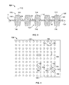
- FIG. 1 is an exploded view of an electronic assembly including a socket connector having an interconnect member formed in accordance with an exemplary embodiment of the present invention.
- FIG. 2 is an enlarged view of a portion of the interconnect member shown in FIG. 1 .
- FIG. 3 is a cross-sectional view of the interconnect member taken along the line 3 - 3 in FIG. 2 .
- FIG. 4 is a top plan view of the insulator shown in FIG. 2 .
- FIG. 1 illustrates an electronic assembly 100 including a socket connector 110 formed in accordance with an exemplary embodiment of the present invention.
- the socket connector 110 is mounted on a circuit board 114 .
- An electronic package 120 is loaded onto the socket connector 110 .
- the electronic package 120 is electrically connected to the circuit board 114 .
- the electronic package may be a chip or module such as, but not limited to, a central processing unit (CPU), microprocessor, or an application specific integrated circuit (ASIC), or the like.
- CPU central processing unit
- ASIC application specific integrated circuit
- the socket connector 110 includes a dielectric housing 116 that is configured to be mounted on the circuit board 114 .
- the housing 116 holds an interconnect member 124 formed in accordance with an exemplary embodiment of the present invention.
- the interconnect member 124 includes a plurality of electrical contacts 126 .
- the electronic package 120 has a mating surface 130 that engages the interconnect member 124 .
- the interconnect member 124 is interposed between contact pads (not shown) on the mating surface 130 of the electronic package 120 and corresponding contact pads (not shown) on the circuit board 114 to provide electrical paths to electrically connect the electronic package 120 to the circuit board 114 .
- FIG. 2 illustrates an enlarged view of a portion of an inter connect member 124 formed in accordance with an exemplary embodiment of the present invention.
- FIG. 3 illustrates a cross-sectional view of the interconnect member 124 taken along the line 3 - 3 in FIG. 2 .
- the interconnect member 124 includes an insulator or carrier 134 on which the contacts 126 are arranged. Each contact 126 comprises a column formed from a conductive polymer and is held in the insulator 134 .
- the conductive polymer is a metallized polymer such as a blend of a polymer and silver powder. In other embodiments, polymers mixed with other conductive materials may be employed.
- the insulator 134 is a substantially planar sheet of non-conductive material having a thickness T between a first side 136 and an opposite second side 138 .
- the first and second sides 136 and 138 are substantially parallel to one another.
- Each contact 126 includes an elongated contact body 140 that extends along a longitudinal axis 142 between first and second opposite ends 144 and 146 .
- the first end 144 extends from the first side 136 of the insulator 134 and a second end 146 extends from the second side 138 of the insulator 134 .
- the contacts 126 provide electrical paths between contact pads (not shown) on the electronic package 120 and corresponding contact pads (not shown) on the circuit board 114 .
- Paths 150 of conductive polymer material are formed in the insulator 134 and extend between two or more pre-selected contact locations in the insulator 134 .
- the paths 150 of conductive polymer material form shorting paths 150 between the selected contact locations.
- the shorting paths 150 effectively short together the contacts 126 along the shorting paths 150 thereby enabling the simulation of solder defects to facilitate the resolution of actual faults and errors as will be described.
- the shorting paths 150 are molded in the insulator 134 and are formed of the same conductive polymer material as the contact 126 .
- the shorting paths 150 are molded onto the insulator 134 simultaneously with the contacts 126 and thus are unitarily formed with the contacts 126 .
- FIG. 4 illustrates a top plan view of the insulator 134 .
- the insulator 134 is formed with a plurality of contact apertures 160 therethrough that define contact locations on the insulator 134 .
- the apertures 160 may be formed by an etching, drilling, or die cutting process or other known methods.
- the contacts 126 FIG. 3
- the contacts 126 FIG. 3
- Shorting channels 164 are formed in the insulator 134 that interconnect two or more pre-selected contact apertures 160 .
- the shorting channels 164 extend at least partially through the insulator 134 and define locations for conductive polymer material that defines the shorting paths 150 ( FIG. 2 ) in the insulator 134 .
- the channels 164 are cut completely through the insulator 134 .
- the insulator 134 is fabricated from a flexible polyimide material, and more specifically, the insulator 134 may be fabricated from a polyimide material that is commonly known as Kapton® which is available from E.I. du Pont de Nemours and Company.
- the interconnect member 124 enables solder fault testing of connectors and electronic packages or chips to be economically performed. During solder fault testing, shorts at specific contact locations may be simulated and the results tracked. The simulated data can then be used to diagnose malfunctions and identify possible solder problem locations.
- the interconnect member 124 is fabricated using a transfer molding process wherein all of the contacts 126 are molded at one time. The shorting paths 150 are formed within the insulator 134 so that separate molds are not required for each shorting scenario.
- the contact apertures 160 are formed in the insulator 134 in a pattern that is complementary to the contact pad patterns (not shown) on the electronic package 120 and the circuit board 114 ( FIG. 1 ). Shorting channels 164 are then cut or routed in the insulator 134 between contact apertures 160 selected for a particular shorting scenario. The contacts 126 and shorting paths 150 are then simultaneously molded on the insulator 134 to complete the fabrication of the interconnect member 124 .
- the embodiments thus described provide a connector that is particularly useful in solder fault testing involving tracking of solder ball shorts and their effects on an associated electronic package.
- the connector can be economically manufactured and provides the capability to simulate solder faults between pre-selected contact locations. Results from the simulated fault testing are tracked and used to identify and resolve actual faults and errors in the electronic package.
Abstract
Description
Claims (20)
Priority Applications (1)
| Application Number | Priority Date | Filing Date | Title |
|---|---|---|---|
| US11/865,788 US7686624B2 (en) | 2007-10-02 | 2007-10-02 | Electrical connector with contact shorting paths |
Applications Claiming Priority (1)
| Application Number | Priority Date | Filing Date | Title |
|---|---|---|---|
| US11/865,788 US7686624B2 (en) | 2007-10-02 | 2007-10-02 | Electrical connector with contact shorting paths |
Publications (2)
| Publication Number | Publication Date |
|---|---|
| US20090088005A1 US20090088005A1 (en) | 2009-04-02 |
| US7686624B2 true US7686624B2 (en) | 2010-03-30 |
Family
ID=40508875
Family Applications (1)
| Application Number | Title | Priority Date | Filing Date |
|---|---|---|---|
| US11/865,788 Active 2027-11-23 US7686624B2 (en) | 2007-10-02 | 2007-10-02 | Electrical connector with contact shorting paths |
Country Status (1)
| Country | Link |
|---|---|
| US (1) | US7686624B2 (en) |
Cited By (4)
| Publication number | Priority date | Publication date | Assignee | Title |
|---|---|---|---|---|
| US11128072B1 (en) | 2020-07-22 | 2021-09-21 | TE Connectivity Services Gmbh | Electrical connector assembly having variable height contacts |
| US20220029325A1 (en) * | 2020-07-22 | 2022-01-27 | TE Connectivity Services Gmbh | Electrical connector assembly having hybrid conductive polymer contacts |
| US20220294145A1 (en) * | 2021-03-09 | 2022-09-15 | TE Connectivity Services Gmbh | Electrical interconnect |
| US11509084B2 (en) | 2020-07-24 | 2022-11-22 | Te Connectivity Solutions Gmbh | Electrical connector assembly having hybrid conductive polymer contacts |
Citations (10)
| Publication number | Priority date | Publication date | Assignee | Title |
|---|---|---|---|---|
| US5599193A (en) | 1994-08-23 | 1997-02-04 | Augat Inc. | Resilient electrical interconnect |
| US6271482B1 (en) | 1994-08-23 | 2001-08-07 | Thomas & Betts International, Inc. | Conductive elastomer interconnect |
| US6348659B1 (en) | 1999-01-07 | 2002-02-19 | Thomas & Betts International, Inc. | Resilient electrical interconnects having non-uniform cross-section |
| US6394853B1 (en) * | 2000-08-04 | 2002-05-28 | Thomas & Betts International, Inc. | Data connector for selective switching between at least two distinct mating connector plugs |
| US6669490B1 (en) | 2002-12-10 | 2003-12-30 | Tyco Electronics Corporation | Conductive elastomeric contact system with anti-overstress columns |
| US20040029411A1 (en) * | 2000-01-20 | 2004-02-12 | Rathburn James J. | Compliant interconnect assembly |
| US6790057B2 (en) | 2002-12-10 | 2004-09-14 | Tyco Electronics Corporation | Conductive elastomeric contact system with anti-overstress columns |
| US6796810B2 (en) * | 2002-12-10 | 2004-09-28 | Tyco Electronics Corporation | Conductive elastomeric contact system |
| US6854985B1 (en) * | 1998-12-16 | 2005-02-15 | Paricon Technologies Corporation | Elastomeric interconnection device and methods for making same |
| US7070420B1 (en) | 2005-08-08 | 2006-07-04 | Wakefield Steven B | Electrical interconnect system utilizing nonconductive elastomeric elements and continuous conductive elements |
-
2007
- 2007-10-02 US US11/865,788 patent/US7686624B2/en active Active
Patent Citations (10)
| Publication number | Priority date | Publication date | Assignee | Title |
|---|---|---|---|---|
| US5599193A (en) | 1994-08-23 | 1997-02-04 | Augat Inc. | Resilient electrical interconnect |
| US6271482B1 (en) | 1994-08-23 | 2001-08-07 | Thomas & Betts International, Inc. | Conductive elastomer interconnect |
| US6854985B1 (en) * | 1998-12-16 | 2005-02-15 | Paricon Technologies Corporation | Elastomeric interconnection device and methods for making same |
| US6348659B1 (en) | 1999-01-07 | 2002-02-19 | Thomas & Betts International, Inc. | Resilient electrical interconnects having non-uniform cross-section |
| US20040029411A1 (en) * | 2000-01-20 | 2004-02-12 | Rathburn James J. | Compliant interconnect assembly |
| US6394853B1 (en) * | 2000-08-04 | 2002-05-28 | Thomas & Betts International, Inc. | Data connector for selective switching between at least two distinct mating connector plugs |
| US6669490B1 (en) | 2002-12-10 | 2003-12-30 | Tyco Electronics Corporation | Conductive elastomeric contact system with anti-overstress columns |
| US6790057B2 (en) | 2002-12-10 | 2004-09-14 | Tyco Electronics Corporation | Conductive elastomeric contact system with anti-overstress columns |
| US6796810B2 (en) * | 2002-12-10 | 2004-09-28 | Tyco Electronics Corporation | Conductive elastomeric contact system |
| US7070420B1 (en) | 2005-08-08 | 2006-07-04 | Wakefield Steven B | Electrical interconnect system utilizing nonconductive elastomeric elements and continuous conductive elements |
Cited By (6)
| Publication number | Priority date | Publication date | Assignee | Title |
|---|---|---|---|---|
| US11128072B1 (en) | 2020-07-22 | 2021-09-21 | TE Connectivity Services Gmbh | Electrical connector assembly having variable height contacts |
| US20220029325A1 (en) * | 2020-07-22 | 2022-01-27 | TE Connectivity Services Gmbh | Electrical connector assembly having hybrid conductive polymer contacts |
| US11509080B2 (en) * | 2020-07-22 | 2022-11-22 | Te Connectivity Solutions Gmbh | Electrical connector assembly having hybrid conductive polymer contacts |
| US11509084B2 (en) | 2020-07-24 | 2022-11-22 | Te Connectivity Solutions Gmbh | Electrical connector assembly having hybrid conductive polymer contacts |
| US20220294145A1 (en) * | 2021-03-09 | 2022-09-15 | TE Connectivity Services Gmbh | Electrical interconnect |
| US11894629B2 (en) * | 2021-03-09 | 2024-02-06 | Tyco Electronics Japan G.K. | Electrical interconnect with conductive polymer contacts having tips with different shapes and sizes |
Also Published As
| Publication number | Publication date |
|---|---|
| US20090088005A1 (en) | 2009-04-02 |
Similar Documents
| Publication | Publication Date | Title |
|---|---|---|
| US7448883B2 (en) | Connector with metalized coated polymer contact | |
| US6062873A (en) | Socket for chip package test | |
| JP4911495B2 (en) | Socket for semiconductor integrated circuit | |
| US8287288B2 (en) | Low profile electrical connector embedded with printed circuit board | |
| US7549871B2 (en) | Connector with dual compression polymer and flexible contact array | |
| US9039425B2 (en) | Electrical interconnect device | |
| US7857631B2 (en) | Socket with a housing with contacts with beams of unequal lengths | |
| KR100602442B1 (en) | Test socket having connecting substrate | |
| US7686624B2 (en) | Electrical connector with contact shorting paths | |
| KR100932459B1 (en) | Contactors and Test Methods Using Contactors | |
| JPH1164425A (en) | Method and device for continuity inspection in electronic part | |
| US7484968B2 (en) | Socket for an electrical tester | |
| JP2856195B2 (en) | Device mounting structure on circuit board | |
| US7692281B2 (en) | Land grid array module with contact locating features | |
| US20070238324A1 (en) | Electrical connector | |
| US7759795B2 (en) | Printed circuit board having reliable bump interconnection structure, method of fabricating the same, and semiconductor package using the same | |
| US20060264096A1 (en) | Surface mount retention module | |
| KR20010050991A (en) | Contact film used for devices having ball grid array structure and device mounting structure | |
| US8530754B2 (en) | Printed circuit board having adaptable wiring lines and method for manufacturing the same | |
| KR100844486B1 (en) | Test socket for semiconductor chip | |
| US20240063562A1 (en) | Electrical connector with integrated ground plane | |
| KR200226638Y1 (en) | Test socket | |
| KR101829327B1 (en) | Connecting device between test board and semiconductor chip | |
| US20140284092A1 (en) | Split pad for circuit board | |
| JPH09270484A (en) | Ic socket |
Legal Events
| Date | Code | Title | Description |
|---|---|---|---|
| AS | Assignment |
Owner name: TYCO ELECTRONICS CORPORATION,PENNSYLVANIA Free format text: ASSIGNMENT OF ASSIGNORS INTEREST;ASSIGNORS:MASON, JEFFREY W.;ALDEN, WAYNE S., III;WAPENSKI, PETER D.;REEL/FRAME:019906/0098 Effective date: 20070917 Owner name: TYCO ELECTRONICS CORPORATION, PENNSYLVANIA Free format text: ASSIGNMENT OF ASSIGNORS INTEREST;ASSIGNORS:MASON, JEFFREY W.;ALDEN, WAYNE S., III;WAPENSKI, PETER D.;REEL/FRAME:019906/0098 Effective date: 20070917 |
|
| STCF | Information on status: patent grant |
Free format text: PATENTED CASE |
|
| FPAY | Fee payment |
Year of fee payment: 4 |
|
| AS | Assignment |
Owner name: TE CONNECTIVITY CORPORATION, PENNSYLVANIA Free format text: CHANGE OF NAME;ASSIGNOR:TYCO ELECTRONICS CORPORATION;REEL/FRAME:041350/0085 Effective date: 20170101 |
|
| MAFP | Maintenance fee payment |
Free format text: PAYMENT OF MAINTENANCE FEE, 8TH YEAR, LARGE ENTITY (ORIGINAL EVENT CODE: M1552) Year of fee payment: 8 |
|
| AS | Assignment |
Owner name: TE CONNECTIVITY SERVICES GMBH, SWITZERLAND Free format text: ASSIGNMENT OF ASSIGNORS INTEREST;ASSIGNOR:TE CONNECTIVITY CORPORATION;REEL/FRAME:056514/0048 Effective date: 20180928 Owner name: TE CONNECTIVITY SERVICES GMBH, SWITZERLAND Free format text: CHANGE OF ADDRESS;ASSIGNOR:TE CONNECTIVITY SERVICES GMBH;REEL/FRAME:056514/0015 Effective date: 20191101 |
|
| MAFP | Maintenance fee payment |
Free format text: PAYMENT OF MAINTENANCE FEE, 12TH YEAR, LARGE ENTITY (ORIGINAL EVENT CODE: M1553); ENTITY STATUS OF PATENT OWNER: LARGE ENTITY Year of fee payment: 12 |
|
| AS | Assignment |
Owner name: TE CONNECTIVITY SOLUTIONS GMBH, SWITZERLAND Free format text: MERGER;ASSIGNOR:TE CONNECTIVITY SERVICES GMBH;REEL/FRAME:060885/0482 Effective date: 20220301 |