US7656446B2 - CCD color solid-state image pickup device - Google Patents
CCD color solid-state image pickup device Download PDFInfo
- Publication number
- US7656446B2 US7656446B2 US10/796,149 US79614904A US7656446B2 US 7656446 B2 US7656446 B2 US 7656446B2 US 79614904 A US79614904 A US 79614904A US 7656446 B2 US7656446 B2 US 7656446B2
- Authority
- US
- United States
- Prior art keywords
- electric charge
- charge storage
- light
- electric charges
- signal
- Prior art date
- Legal status (The legal status is an assumption and is not a legal conclusion. Google has not performed a legal analysis and makes no representation as to the accuracy of the status listed.)
- Expired - Fee Related, expires
Links
- 238000003860 storage Methods 0.000 claims abstract description 133
- 239000000758 substrate Substances 0.000 claims abstract description 78
- 238000012546 transfer Methods 0.000 claims abstract description 74
- 239000004065 semiconductor Substances 0.000 claims abstract description 50
- 238000005036 potential barrier Methods 0.000 claims abstract description 7
- 239000002019 doping agent Substances 0.000 claims description 18
- XUIMIQQOPSSXEZ-UHFFFAOYSA-N Silicon Chemical compound [Si] XUIMIQQOPSSXEZ-UHFFFAOYSA-N 0.000 claims description 12
- 229910052710 silicon Inorganic materials 0.000 claims description 12
- 239000010703 silicon Substances 0.000 claims description 12
- 239000012535 impurity Substances 0.000 claims description 6
- 230000003287 optical effect Effects 0.000 claims description 6
- 238000013459 approach Methods 0.000 claims description 3
- 239000010410 layer Substances 0.000 description 113
- 239000003086 colorant Substances 0.000 description 18
- 238000006243 chemical reaction Methods 0.000 description 11
- 230000035945 sensitivity Effects 0.000 description 10
- 238000002955 isolation Methods 0.000 description 7
- 229910021420 polycrystalline silicon Inorganic materials 0.000 description 7
- 229920005591 polysilicon Polymers 0.000 description 7
- 230000003595 spectral effect Effects 0.000 description 7
- VYPSYNLAJGMNEJ-UHFFFAOYSA-N Silicium dioxide Chemical compound O=[Si]=O VYPSYNLAJGMNEJ-UHFFFAOYSA-N 0.000 description 6
- 238000000034 method Methods 0.000 description 6
- 238000012545 processing Methods 0.000 description 6
- 230000031700 light absorption Effects 0.000 description 5
- 229910052785 arsenic Inorganic materials 0.000 description 4
- 229910052681 coesite Inorganic materials 0.000 description 3
- 230000000295 complement effect Effects 0.000 description 3
- 229910052906 cristobalite Inorganic materials 0.000 description 3
- 230000002708 enhancing effect Effects 0.000 description 3
- 230000001965 increasing effect Effects 0.000 description 3
- 239000000463 material Substances 0.000 description 3
- 239000000377 silicon dioxide Substances 0.000 description 3
- 229910052682 stishovite Inorganic materials 0.000 description 3
- 229910052905 tridymite Inorganic materials 0.000 description 3
- ZOXJGFHDIHLPTG-UHFFFAOYSA-N Boron Chemical compound [B] ZOXJGFHDIHLPTG-UHFFFAOYSA-N 0.000 description 2
- RQNWIZPPADIBDY-UHFFFAOYSA-N arsenic atom Chemical compound [As] RQNWIZPPADIBDY-UHFFFAOYSA-N 0.000 description 2
- 229910052796 boron Inorganic materials 0.000 description 2
- 230000007547 defect Effects 0.000 description 2
- BHEPBYXIRTUNPN-UHFFFAOYSA-N hydridophosphorus(.) (triplet) Chemical compound [PH] BHEPBYXIRTUNPN-UHFFFAOYSA-N 0.000 description 2
- 230000014759 maintenance of location Effects 0.000 description 2
- 230000002093 peripheral effect Effects 0.000 description 2
- 230000008569 process Effects 0.000 description 2
- 230000009467 reduction Effects 0.000 description 2
- 230000008901 benefit Effects 0.000 description 1
- 230000005540 biological transmission Effects 0.000 description 1
- 238000001444 catalytic combustion detection Methods 0.000 description 1
- 230000001419 dependent effect Effects 0.000 description 1
- 238000013461 design Methods 0.000 description 1
- 230000006866 deterioration Effects 0.000 description 1
- 230000003467 diminishing effect Effects 0.000 description 1
- 238000009826 distribution Methods 0.000 description 1
- 238000005562 fading Methods 0.000 description 1
- 238000002347 injection Methods 0.000 description 1
- 239000007924 injection Substances 0.000 description 1
- 239000011229 interlayer Substances 0.000 description 1
- 238000004519 manufacturing process Methods 0.000 description 1
- 239000000203 mixture Substances 0.000 description 1
- 239000000049 pigment Substances 0.000 description 1
- 230000000750 progressive effect Effects 0.000 description 1
- 230000004044 response Effects 0.000 description 1
Images


Classifications
-
- H—ELECTRICITY
- H01—ELECTRIC ELEMENTS
- H01L—SEMICONDUCTOR DEVICES NOT COVERED BY CLASS H10
- H01L27/00—Devices consisting of a plurality of semiconductor or other solid-state components formed in or on a common substrate
- H01L27/14—Devices consisting of a plurality of semiconductor or other solid-state components formed in or on a common substrate including semiconductor components sensitive to infrared radiation, light, electromagnetic radiation of shorter wavelength or corpuscular radiation and specially adapted either for the conversion of the energy of such radiation into electrical energy or for the control of electrical energy by such radiation
- H01L27/144—Devices controlled by radiation
- H01L27/146—Imager structures
- H01L27/148—Charge coupled imagers
- H01L27/14868—CCD or CID colour imagers
-
- H—ELECTRICITY
- H01—ELECTRIC ELEMENTS
- H01L—SEMICONDUCTOR DEVICES NOT COVERED BY CLASS H10
- H01L27/00—Devices consisting of a plurality of semiconductor or other solid-state components formed in or on a common substrate
- H01L27/14—Devices consisting of a plurality of semiconductor or other solid-state components formed in or on a common substrate including semiconductor components sensitive to infrared radiation, light, electromagnetic radiation of shorter wavelength or corpuscular radiation and specially adapted either for the conversion of the energy of such radiation into electrical energy or for the control of electrical energy by such radiation
- H01L27/144—Devices controlled by radiation
- H01L27/146—Imager structures
- H01L27/148—Charge coupled imagers
- H01L27/14806—Structural or functional details thereof
- H01L27/14812—Special geometry or disposition of pixel-elements, address lines or gate-electrodes
- H01L27/14818—Optical shielding
-
- H—ELECTRICITY
- H04—ELECTRIC COMMUNICATION TECHNIQUE
- H04N—PICTORIAL COMMUNICATION, e.g. TELEVISION
- H04N25/00—Circuitry of solid-state image sensors [SSIS]; Control thereof
Definitions
- the present invention relates to a CCD (charge-coupled device) color solid-state image pickup device.
- color filters having different spectral transmission coefficients are stacked on a plurality of photodiodes arranged in a two-dimensional array, thereby enabling pickup of a color image.
- a B filter In the color filters [red (R), green (G), and blue (B)] of primary color system, for instance, a B filter primarily permits passage of only light having a short wavelength of 470 nm or less. Hence, a photodiode of a light-receiving section with the B filter stacked thereon has sensitivity to B incident light. However, the B filter blocks light having other wavelength components (e.g., G and R), and hence G and R wavelength components that have entered the B filter are not subjected to photoelectric conversion. Thus, color filters of this type suffer a problem of a failure to effectively utilize all wavelength components.
- a yellow (Ye) filter permits arrival of light of G and R wavelengths at a photodiode of a corresponding light-receiving section
- a cyan (Cy) filter permits arrival of light of B and G wavelengths at a photodiode of a corresponding light-receiving section
- a magenta (Mg) filter permits arrival of light of B and R wavelengths at a photodiode of a corresponding light-receiving section.
- a signal output from each photodiode of the solid-state image pickup device using the color filters of complementary color system includes a mixture of a plurality of color signals, such as G and R, B and G, and B and R.
- an external signal processing circuit must perform processing for separating the signal into R, G, and B color signals. Accordingly, there is a problem that an image photographed and reproduced by a solid-state image pickup device using color filters of complementary color system is usually inferior in quality to that photographed and reproduced by a solid-state image pickup device using color filters of primary color system, in terms of color reproducibility, signal noise, or the like. Therefore, a digital still camera which photographs a still image frequently employs a solid-state image pickup device using color filters of primary color system.
- the light absorption coefficient of a silicon substrate changes across a visible range from light of long wavelength (R) to light of short wavelength (B). Therefore, light of a wavelength range having a large light absorption coefficient is absorbed by a shallow area of the silicon substrate, and hence the light hardly reaches a deep area of the silicon substrate. Conversely, light of a wavelength range having a small light absorption coefficient reaches a deep region of the silicon substrate. Therefore, photoelectric conversion can be performed even at the deep area of the silicon substrate.
- Publication 1 “A Planar Silicon Photosensor with an Optimal Spectral Response for Detecting Printed Material” by Paul A. Gary and John G. Linvill, IEEE TRANSACTIONS ON ELECTRON DEVICES, Vol. ED-15, No. 1, Jan. 1968. (hereinafter referred to as “Publication 1”) describes dependence of a photoelectric conversion characteristic of a photodiode on the depthwise position of a silicon substrate as well as on the wavelength of incident light.
- the solid-state color imager with three photo-sensitive layers of U.S. Pat. No. 4,438,455 configured on the principle described in Publication 1 has a structure for extracting signals of three colors; i.e., R, G, and B. Without using color filters over-laid on the photo-sensitive elements, no light absorption of color filter material has arisen, and hence, incident light can be effectively converted into an electric signal.
- U.S. Pat. No. 4,438,455 describes a structure 101 embodied by means of superimposing three photo-sensitive layers 102 , 103 , 104 and changing the depth of each photo-conductive layer against the incident light to apply the principle described in Publication 1 to the above structure.
- the solid-state color imager of JP-A-1-134966 configured on the principle described in Publication 1 has a structure of three story N + P photo-diode with different depth for extracting signals of three colors; i.e., R, G, and B, from one pixel. Without using color filters over-laid on the photo-diode elements, no light absorption of color filter material has arisen, and hence, incident light can be effectively converted into electric signal. Further, false signals or false colors, such as moiré, can be improved.
- JP-A-1-134966 describes a structure embodied by means of changing the depth of each N + P photo-diode to apply the principle described in Publication 1 to the above structure.
- short wavelength light such as Blue is detected by the shallow N + P photo-diode 201 .
- Long wavelength light such as Red is detected by the deep N + P photo-diode 203 as shown in FIG. 24C .
- the medium wavelength light such as Green is detected by the N + P photo-diode 202 locating in the depth of between the above two N + P photo-diodes as shown in FIG. 24B .
- one reading gate section and one vertical transfer stage are associated with one light-reading section.
- the area of the electric charge transfer path other than the light-receiving section is covered with a transfer-electrode. Therefore, no electrical contacts are provided in the light-receiving area, and no other peripheral circuits are provided for each pixel. Therefore, in the related-art CCD structure, signals corresponding to two or more different spectral sensitivities are read from one light-receiving section by utilization of a depthwise optical characteristic of the semiconductor substrate described in Publication 1. The signals cannot be subjected directly to charge transfer operation.
- the present invention aims at providing a CCD color solid-state image pickup device capable of separately reading signal electric charges of a plurality of different colors from one pixel (light-receiving section) by utilization of a depthwise optical characteristic of a semiconductor substrate.
- the present invention provides a CCD color solid-state image pickup device comprising: a plurality of light-receiving sections arranged in an array on the surface of a semiconductor substrate; and a vertical transfer path by way of which signal electric charges stored in electric charge storage sections of the respective light-receiving sections are read and transferred to a horizontal transfer path, wherein the electric charge storage section of each of the light-receiving sections has a plurality of electric charge storage layers which are provided in a depthwise direction of the semiconductor substrate with potential barriers interposed therebetween; and signal electric charges stored in the respective electric charge storage layers are read independently to the vertical transfer path.
- an electric charge path which causes electric charges stored in the electric charge storage layers to migrate to the surface of the semiconductor substrate and is formed from a heavily-doped impurity region, may be provided in an electric charge storage layer from among the plurality of electric charge storage layers, the electric charge storage-layer being provided in the semiconductor substrate.
- a concentration gradient may be imparted such that the dopant concentration of the electric charge storage layers formed as heavily-doped impurity regions and the dopant concentration of the electric charge path continually connected to the electric charge storage layer increase as the electric charge storage layer and the electric charge path approach the vertical transfer path.
- the depths of the respective electric charge storage layers may be set in accordance with wavelengths of incident light to be detected.
- spectral characteristics of the respective electric charge storage layers can be rendered as originally set.
- the CCD color solid-state image pickup device of the invention may be arranged in a manner that three electric charge storage layers may be provided as the plurality of electric charge storage layers; an electric charge storage layer provided at the deepest location from among the three electric charge storage layers stores signal electric charges corresponding to red (R) incident light; an electric charge storage disposed in a surface section stores signal electric charges corresponding to blue (B) incident light; and an electric charge storage layer provided at an intermediate section stores signal electric charges corresponding to green (G) incident light.
- three signals of the primary colors can be detected from one light-receiving section.
- the depth of the electric charge storage layer provided in the surface section may range from 0.2 to 0.4 ⁇ m; the depth of the electric charge storage layer provided in the intermediate section may range from 0.4 to 0.8 ⁇ m; and the depth of the electric charge storage layer provided in the deepest section may range from 0.8 to 2.5 ⁇ m.
- the depths of the respective electric charge storage layers are made optimal for detecting R, G, and B incident light beams.
- a first light-receiving section for storing blue (B) and green (G) signal electric charges and a second light-receiving section for storing signal green (G) and red (R) signal electric charges may be alternately provided as the light-receiving sections on the surface of the semiconductor substrate; the first light-receiving section may be provided with a first electric charge storage layer for storing blue (B) signal electric charges and a second electric charge storage layer for storing green (G) signal electric charges; and the second light-receiving section may be provided with a second electric charge storage layer for storing green (G) signal electric charges and a third electric charge storage layer for storing red (R) signal electric charges.
- signal electric charges can be detected on a per-color basis without color filters.
- the depth of the first electric charge storage layer may range from 0.2 to 0.4 ⁇ m; the depth of the second electric charge storage layer may range from 0.4 to 0.8 ⁇ m; and the depth of the third electric charge storage layer may range from 0.8 to 2.5 ⁇ m.
- on-chip light gathering optical systems may be provided on upper portions of the respective light-receiving sections, and one opening of each light-shielding film may correspond to one of the light-receiving sections.
- the light-receiving section may be provided with a first electric storage layer for storing blue (B) signal electric charges and a second electric charge storage layer for storing green (G) signal electric charges; and electric charges stored in the vertical transfer path may be used as signal electric charges corresponding to red (R) incident light.
- a polysilicon electrode layer superimposed on the vertical transfer path absorbs light of a wavelength of 580 nm or less.
- the electric charge transfer path can be utilized as a photoelectric conversion area, and hence a high-sensitivity CCD solid-state image pickup device can be implemented without use of a microlens.
- the depth of the first electric charge storage layer may range from 0.2 to 0.4 ⁇ m; and the depth of the second electric charge storage layer may range from 0.4 to 0.8 ⁇ m.
- the light-receiving sections may be arranged in a square grid pattern on the surface of the semiconductor substrate. In the CCD color solid-state image pickup device of the present invention, the light-receiving sections may be arranged in a honeycomb pattern on the surface of the semiconductor substrate. The present invention can be applied to any of these pixel arrangements.
- FIG. 1 is a schematic surface view of a CCD color solid-state image pickup device according to a first embodiment of the invention
- FIG. 2 is a descriptive view for reading signal electric charges from the color solid-state image pickup device of the first embodiment
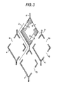
- FIG. 3 is a plan view showing four pixels, each pixel corresponding to the light-receiving section shown in FIG. 1 , and a detailed pattern of a vertical transfer path laid between the light-receiving sections;
- FIG. 4 is a view made by superimposing transfer electrodes on the pattern shown in FIG. 3 ;
- FIG. 5 is a detailed view of the inside of an area V enclosed by a circle shown in FIG. 4 ;
- FIG. 6A is a cross-sectional view taken along line a-a shown in FIG. 4 ;
- FIG. 6B is a cross-sectional view taken along line b-b shown in FIG. 4 ;
- FIG. 6C is a cross-sectional view taken along line c-c shown in FIG. 4 ;
- FIG. 7 is a view showing the range in which a surface P + layer is to be formed within the light-receiving section of the first embodiment
- FIG. 8 is a view showing the potential profile of the light-receiving section of the first embodiment in the depthwise direction of the substrate;
- FIG. 9 is a view showing wavelength dependence of a photoelectric conversion characteristic of the light-receiving section of the first embodiment
- FIG. 10 is a schematic surface view of a CCD color solid-state image pickup device according to a second embodiment of the invention.
- FIG. 11 is a descriptive view for reading signal electric charges from the color solid-state image pickup device of the second embodiment
- FIG. 12 is a plan view showing two unit pixels of the second embodiment and a vertical transfer path laid between the pixels;
- FIG. 13 is a view showing a transfer electrode of the color solid-state image pickup device of the second embodiment
- FIG. 14A is a cross-sectional view taken along line a-a shown in FIG. 13 ;
- FIG. 14B is a cross-sectional view taken along line b-b shown in FIG. 13 ;
- FIG. 15A is a view showing the potential profile of the light-receiving section shown in FIG. 14A in the depthwise direction of the substrate;
- FIG. 15B is a view showing the potential profile of the light-receiving section shown in FIG. 14B in the depthwise direction of the substrate;
- FIG. 16 is a schematic surface view of a CCD color solid-state image pickup device according to a third embodiment of the invention.
- FIG. 17 is a descriptive view for reading signal electric charges from the color solid-state image pickup device of the third embodiment.
- FIG. 18 is a plan view of four pixels of the color solid-state image pickup device of the third embodiment.
- FIG. 19A is a cross-sectional view taken along line a-a shown in FIG. 18 ;
- FIG. 19B is a cross-sectional view taken, along line b-b shown in FIG. 18 ;
- FIG. 20 is a view showing the potential profile of the light-receiving section of the third embodiment in the depthwise direction of the substrate;
- FIG. 21 is a view showing wavelength dependence of a photoelectric conversion characteristic of the light-receiving section of the third embodiment
- FIG. 22 is a cross-sectional view of one unit pixel (light-receiving section) of a color solid-state image pickup device according to a fourth embodiment of the invention.
- FIG. 23 is a descriptive view of a related-art color solid-state image pickup device.
- FIGS. 24A to 24C are descriptive views of a related-art color solid-state image pickup device.
- FIG. 1 is a schematic surface view of a CCD color solid-state image pickup device according to a first embodiment of the invention.
- a plurality of light-receiving sections 1 are arranged in an array on the surface of a semiconductor substrate.
- each light-receiving section 1 is depicted as a rhombus and acts as a unit pixel.
- the arrangement of pixels employed in the present embodiment corresponds to the arrangement of pixels described in JP-A-10-136391; that is, a so-called honeycomb pixel arrangement in which the respective light-receiving sections 1 are offset at half a pitch in both the vertical and horizontal directions.
- a vertical transfer path e.g., a vertical charge-coupled device (VCCD)] 2 is formed between adjacent light-receiving sections 1 , and signal electric charges read to the vertical transfer path 2 from the respective light-receiving sections 1 are downwardly transferred, in a meandering manner, to a horizontal transfer path [e.g., a horizontal charge-coupled device (HCCD)] 3 .
- VCCD vertical charge-coupled device
- each light-receiving section 1 stores signal electric charges of three colors, i.e., red (R), green (G), and blue (B), and signal electric charges of the respective colors are read separately to the vertical transfer path 2 .
- R/G/B is entered in each light-receiving section 1 .
- this description shows that each unit pixel can subject any of R, G, and B wavelength components to photoelectric conversion and does not mean presence of a color-filter or another structure.
- color components that is, R, G, and B
- R, G, and B are sequentially read from each light-receiving section 1 in an amount corresponding to a total number of pixels; in other words, three surfaces (or three frames).
- the thus-read color components are subjected to signal processing performed by an external circuit, thereby outputting an image signal of a corresponding unit pixel.
- FIG. 3 is a plan view showing four pixels, each pixel corresponding to one of the light-receiving sections 1 shown in FIG. 1 , and a detailed pattern of a vertical transfer path 2 laid between the light-receiving sections 1 .
- Each light-receiving section 1 is partitioned by a rhombus element isolation region 4 .
- gate sections 4 r , 4 g , and 4 b are formed in three sides where the element isolation region 4 is broken.
- An R signal electric charge is read from the gate section 4 r to the vertical transfer path 2 ; a G signal electric charge is read from the gate section 4 g to the vertical transfer path 2 ; and a B signal electric charge is read from the gate section 4 b to the vertical transfer path 2 .
- FIG. 4 is a view made by superimposing transfer electrodes on the pattern shown in FIG. 3 .
- FIG. 5 is a detailed view of the inside of the area V enclosed by a circle shown in FIG. 4 .
- a transfer electrode formed from a two-layer polysilicon structure is superposed on the vertical transfer path 2 .
- Four transfer electrodes 5 , 6 , 7 , and 8 are assigned to one light-receiving section 1 .
- a CCD capable of performing a so-called all pixel reading operation (progressive operation).
- FIG. 6A is a cross-sectional view taken along line a-a shown in FIG. 4 ;
- FIG. 6B is a cross-sectional view taken along line b-b shown in FIG. 4 ;
- FIG. 6C is a cross-sectional view taken along line c-c shown in FIG. 4 .
- the CCD color solid-state image pickup device of the present embodiment is fabricated in an n-type semiconductor substrate 10 .
- a P well layer 11 is formed in the surface of the semiconductor substrate 10 .
- Three N + layers 12 , 13 , and 14 are formed within the P well layer 11 so as to be separated from each other in the depthwise direction of the substrate.
- the N + layer 12 of the surface section extends up to a read gate electrode 6 a formed from a portion of the transfer electrode.
- the signal electric charges primarily produced from an incident light component of short wavelength light (e.g., B) are stored in the N + layer 12 provided at the most shallow position with respect to the depthwise direction of the semiconductor substrate 10 .
- the N + layer 12 ⁇ dopant [phosphorous or arsenic (P or As)] concentration is about 5 ⁇ 10 16-17 /cm 3
- the depth of the N + layer is 0.2 to 0.4 ⁇ m, wherein the depth is dependent on the dopant concentration, and the same also applies to any counterparts in the following descriptions ⁇ constituting the signal electric charge storage section extends up to a position below a read gate section; that is, the read gate electrode 6 a formed from a portion of the transfer electrode 6 .
- an N + layer 13 provided at an intermediate position has, at an end section thereof, an N + region (i.e., a charge path) 13 a which extends up to the surface of the semiconductor substrate 10 .
- This N + region 13 a extends up to a position below a read gate electrode 7 a formed from a portion of the transfer electrode 7 .
- the signal electric charges formed from light of intermediate wavelength (e.g., G) are stored in the N + layer 13 .
- the N + layer 13 (dopant concentration is about 5 ⁇ 10 16-17 /cm 3 at a depth of 0.4 to 0.8 ⁇ m) constituting the storage section extends up to a position below the read gate electrode 7 a .
- the electric charges derived primarily from the light of intermediate wavelength (G) pass through the gate section 4 g shown in FIG. 3 and are read to the vertical transfer path 2 .
- an N + layer 14 formed at the deepest position has, at an end section thereof, an N + region (i.e., a charge path) 14 a which extends up to the surface of the semiconductor substrate 10 .
- This N + region 14 a extends up to a position below a read gate electrode 6 b formed from a portion of the transfer electrode 6 .
- the signal electric charges formed from light of long wavelength e.g., R
- the N + layer 14 (dopant concentration is about 5 ⁇ 10 16-17 /cm 3 at a depth of 0.8 to 2.5 ⁇ m) constituting the storage section extends up to a position below the read gate section.
- the electric charges derived primarily from the light of a long wavelength (R) pass through the gate section 4 r shown in FIG. 3 and are read to the vertical transfer path 2 .
- the CCD color solid-state image pickup device of the embodiment has a three-layer storage section in the depthwise direction of the semiconductor substrate 10 . Depths of the respective storage sections are determined such that the storage sections act as signal electric charge storage sections corresponding to light of B, G, and R colors in a sequence of increasing depth.
- a shallow P + layer 15 is provided in a portion of the surface of the semiconductor substrate 10 having the three-layer storage sections 12 , 13 , and 14 .
- An SiO 2 film 16 is provided on top of the semiconductor substrate 10 .
- Dopant (boron) concentration of the P + layer 15 is about 1 ⁇ 10 18 /cm 3 , and the depth of the P + layer 15 ranges from 0.1 to 0.2 ⁇ m or thereabouts. The dopant concentration contributes to a reduction in a defect level of an oxide film-semiconductor boundary surface. Accordingly, the storage section 12 located at the most shallow position in the depthwise direction of the semiconductor substrate 10 assumes a P + N + P structure.
- the CCD color solid-state image pickup device of the embodiment as a whole assumes a P + (N + P) (N + P) (N + P) structure.
- Three storage sections i.e., N + layers
- a P region which is to become a potential barrier
- the boron concentration of the P region located between the N + layers is set to 1 ⁇ 10 14-16 /cm 3 .
- the dopant concentration of the storage section is preferably given a concentration gradient so as to become higher toward the read gate section than at the light incidence region close to the center of the storage section.
- the dopant concentration of the storage section is preferably given a concentration gradient so as to become higher toward the read gate section than at the light incidence region close to the center of the storage section.
- FIG. 8 is a view showing the potential profile of the light-receiving section 1 in the depthwise direction of the substrate.
- Electric charges produced by light (B) of a short wavelength are chiefly stored in the most shallow electric charge storage section (i.e., the N + layer 12 indicated by “n 1 ” in FIG. 8 ).
- Electric charges produced by light (G) of an intermediate wavelength are chiefly stored in the next shallow electric charge storage section (i.e., the N + layer 13 indicated by “n 2 ” in FIG. 8 ).
- Electric charges produced by light (R) of a long wavelength are chiefly stored in the deepest electric charge storage section (i.e., the N + layer 14 indicated by “n 3 ”, in FIG. 8 ).
- the P region serving as a potential barrier exists between the electric charge storage sections n 1 and n 2 and between the electric charge storage sections n 2 and n 3 .
- Signal charges (i.e., electrons) having developed in the P region are allocated to any of the adjacent charge storage sections (n 1 , n 2 , n 3 ) along the potential profile.
- FIG. 9 is a view showing wavelength dependence of a photoelectric conversion characteristic of the light-receiving section 1 of the embodiment.
- R, G, and B spectral characteristics have characteristics depicted by separated peaks.
- the vertical axis represents relative sensitivity with reference to G.
- the CCD color solid-state image pickup device of the embodiment light of three colors, R, G, and B, is received by one unit pixel (i.e., the light-receiving section 1 ). Electric charges corresponding to respective colors can be stored, thereby obviating a necessity for use of color filters and enabling effective utilization of incident light. Further, three colors, R, G, and B, are independently, separately read. Hence, there is no necessity for addition of new contact sections, new signal lines, and other new peripheral circuits, except that the storage sections n 1 , n 2 , and n 3 and paths for electric charges thereof are provided in the depthwise direction of the substrate and portions of the element isolation region laid around the light-receiving section are used as read gate sections.
- One unit pixel can read all the three colors R, G, and B, and hence the space between unit pixels can be reduced, thereby improving moiré, a false signal, and a false color.
- FIG. 10 is a schematic surface view of a CCD color solid-state image pickup device according to a second embodiment of the invention.
- a light-receiving section 21 is represented by a rectangle and taken as a unit pixel.
- a plurality of light-receiving sections 21 are arranged in an array pattern.
- the light-receiving sections 21 are arranged in a square grid pattern.
- a vertical transfer path 22 is formed between horizontally-adjacent light-receiving sections 21 . Signal charges read from the light-receiving section 21 to the vertical transfer path 22 are transferred to a horizontal transfer path 23 provided at a downward location.
- G/R and G/B are entered in each light-receiving section 21 .
- these descriptions show that each unit pixel can subject R, G wavelength components and B, G wavelength components of the incident light to photoelectric conversion performed in the light-receiving section; the descriptions do not indicate presence of a color filter or another structure.
- the image pickup device has two kinds of light-receiving sections; that is, a light-receiving section capable of storing and reading G, R signal electric charges, and another light-receiving section capable of storing and reading G, B signal electric charges. These light-receiving sections are alternately arranged in both the vertical and horizontal directions.
- a G signal is produced from all the light-receiving sections 21 .
- the R, B signals are alternately arranged in the form of a two-dimensional plane.
- G information corresponding to the total number of pixels i.e., m ⁇ n pixels
- Information corresponding to B and R which are substantially equal in number and arranged alternately (i.e., m ⁇ n pixels)
- the thus-output information items are subjected to signal processing at corresponding pixel positions, thereby forming a color image.
- FIG. 12 is a plan view showing two unit pixels (i.e., the light-receiving sections 21 ) of the embodiment and a vertical transfer path laid between the unit pixels. Each unit pixel is surrounded by a C-shaped element isolation region 24 . Signal electric charges are read to the vertical transfer path 22 from a gate section 24 a where the element isolation region 24 is not present.
- FIG. 13 is a view showing a transfer electrode of the color solid-state image pickup device of the embodiment.
- transfer electrodes 25 , 26 , and 27 have a triple-layer polysilicon structure and are constituted of interline CCDs which can read all pixels.
- the second polysilicon electrode 26 and the third polysilicon electrode 27 constitute read gate electrodes, respectively. When a read voltage is applied to the respective read gate electrodes, a signal electric charge is read to the vertical transfer path 22 from a corresponding signal electric charge storage section.
- FIG. 14A is a cross-sectional view taken along line a-a shown in FIG. 13 ; and FIG. 14B is a cross-sectional view taken along line b-b shown in FIG. 13 .
- a color solid-state image pickup device of the present embodiment has G/B light-receiving sections and G/R light-receiving sections.
- FIG. 14A shows a cross-sectional structure of the G/B light-receiving section; and
- FIG. 14B shows a cross-sectional structure of the G/R light-receiving section.
- a P well layer 31 is formed in the surface of an n-type semiconductor substrate 30 , and two N + layers 32 , 33 are formed within the P well layer 31 so as to be separated from each other in the depthwise direction of the substrate.
- the N + layer 32 ⁇ dopant [phosphorous or arsenic (P or As)] concentration is about 5 ⁇ 10 16-17 /cm 3 ⁇ located in the surface section extends up to a position below the read gate electrode 26 a formed from a portion of the transfer electrode.
- the electric charges derived primarily from the light of short wavelength e.g., B
- the electric charges stored in the storage section 32 that is, only the electric charges produced primarily from light of a short wavelength, are read to the vertical transfer path 22 .
- a second N + layer 33 (dopant concentration is about 5 ⁇ 10 16-17 /cm 3 ) has, at an end section thereof, an N + region (i.e., a charge path) 33 a which extends up to the surface of the semiconductor substrate 30 .
- the N + region 33 a extends up to a position below a read gate electrode 27 a formed from a portion of the transfer electrode.
- the signal electric charges formed from light of intermediate wavelength e.g., G
- the electric charges stored in the storage section 33 that is, only the electric charges produced primarily from light of an intermediate wavelength (G), are read to the vertical transfer path 22 .
- the P well layer 31 is formed in the surface of the n-type semiconductor substrate 30 , and three N + layers 32 , 33 , and 34 are formed within the P well layer 31 so as to be separated from each other in the depthwise direction of the substrate.
- the surface N + layer 32 is not used by the G/R light-receiving section.
- a shallow P + layer 35 is provided in the surface, and a SiO 2 film 36 is further provided in the topmost surface of the substrate, thereby diminishing a defect level of an oxide film-semiconductor boundary surface in the surface of the light-receiving section.
- the second N + layer 33 (dopant concentration is about 5 ⁇ 10 16-17 /cm 3 ) has, at an end section thereof, the N + region (i.e., a charge path) 33 a which extends up to the surface of the semiconductor substrate 30 .
- the N + region 33 a extends up to a position below the read gate electrode formed from a portion of the transfer electrode.
- the signal electric charges formed from light of intermediate wavelength (e.g., G) are stored in the N + layer 33 .
- the electric charges stored in the storage section that is, the electric charges produced primarily from light of an intermediate wavelength (G); are read to the vertical transfer path 22 .
- a third N + layer 34 formed in the deepest section has, at an end section thereof, the N + region (i.e., a charge path) 34 a which extends up to the surface of the semiconductor substrate 30 .
- the N + region 34 a extends up to a position below the read gate electrode 27 a formed from a portion of the transfer electrode.
- the signal electric charges formed from light of a long wavelength e.g., R
- R the signal electric charges formed from light of a long wavelength
- the N + layer 34 dopant concentration is about 5 ⁇ 10 16-17 /cm 3 ), which constitutes the storage section, extending up to a position located below the read gate, the electric charges produced primarily from light of a long wavelength (R) are read to the vertical transfer path 22 .
- the G/R light-receiving section does not detect signal electric charges produced by the light (B) of a short wavelength as a signal. Hence, there is no necessity for reading electric charges from the first N + layer 32 located at the most shallow position with respect to the depth wise direction of the substrate. Since the electric charges stored in the N + layer 32 are no necessary, the electric charges are withdrawn to the outside from the substrate 30 by application of a bias voltage to the substrate 30 .
- the G/B light-receiving section does not detect as a signal electric charges produced by the light (R) of a long wavelength.
- the N + layer 34 for detecting R signal electric charges is not formed.
- the N + layer 34 may be formed but arranged not to read electric charges stored therein.
- two or three layers of signal electric charge storage sections are provided in the depthwise direction of the semiconductor substrate. Hence, signal electric charges corresponding the quantity of respective R, G, and B light can be stored and read separately, thereby enabling effective utilization of incident light.
- FIG. 15A is a view showing the potential profile of the G/B light-receiving section of the embodiment in the depthwise direction of the substrate.
- FIG. 15B is a view showing the potential profile of the G/R light-receiving section of the embodiment in the depthwise direction of the substrate.
- Electric charges produced by light (B) of a short wavelength are chiefly stored in the most shallow electric charge storage section (i.e., the N + layer 32 indicated by “n 1 ” in FIG. 15 ).
- Electric charges produced by light (G) of an intermediate wavelength are chiefly stored in the next shallow electric charge storage section (i.e., the N + layer 33 indicated by “n 2 ” in FIG. 15 ).
- Electric charges produced by light (R) of a long wavelength are chiefly stored in the deepest electric charge storage section (i.e., the N + layer 34 indicated by “n 3 ” in FIG. 15 ).
- the P well layer 31 and the n-type semiconductor substrate 30 are situated at positions further below the deepest electric charge storage section. Hence, excessive electric charges, particularly, electric charges caused by light of a wavelength longer than R, flow toward the substrate.
- Wavelength dependence of a photoelectric conversion characteristic of the color solid-state image pickup device of the embodiment is identical with that shown in FIG. 9 in connection with the first embodiment.
- FIG. 15A the storage section n 3 corresponding to R is not formed, and hence a corresponding potential well is not present.
- FIG. 15B a storage section corresponding to the storage section n 1 ; that is, B, is formed.
- stored electric charges are not read to the vertical transfer path.
- a high voltage is applied to the substrate 30 , thereby withdrawing the electric charges stored in the storage section n 1 until the storage section n 1 enters an initial state (i.e., an empty state).
- FIG. 16 is a schematic surface view of a CCD color solid-state image pickup device according to a third embodiment of the invention.
- the basic configuration of the present embodiment is analogous to that of the first embodiment.
- the present embodiment differs in that a light-receiving section 40 of the present embodiment detects signal electric charges of two colors; that is, G and B and that a vertical-transfer path 41 per se is utilized as an R light receiving region.
- the concept for utilizing the vertical transfer path 41 as a region for receiving light of a long wavelength (R) has already been known as described in, e.g., Japanese Patent No. 2534105.
- the vertical transfer path 41 is used as a light-receiving region for receiving light of a long wavelength (R).
- the original light-receiving section 40 can be configured to output information about B and G. More specifically, as shown in FIG. 17 , only light of a long wavelength (R) of the light having entered the vertical transfer path passes through a transfer electrode layer formed from polysilicon and then reaches the silicon substrate, thereby producing electric charges within the vertical transfer path. First, the thus-produced electric charges are transferred vertically and read.
- the signal serves as data corresponding to a total number of pixels (m ⁇ n) concerning R.
- the signal electric charges pertaining to G and B are read from the light-receiving section.
- the thus-read electric charges are twice transferred vertically and horizontally, to thereby produce signal data.
- the R, G, and B signals are subjected to signal processing as single pixel position information.
- FIG. 18 is a plan view of four pixels of a color solid-state image pickup device of the embodiment.
- the respective light-receiving sections 40 of the embodiment are partitioned by rhombus element isolation regions 42 .
- gate sections 42 g , 42 b are formed in two right sides of the element isolation region 42 .
- a G signal electric charge is read to the vertical transfer path 41 by way of the gate section 42 g
- a B signal electric charge is read to the vertical transfer path 41 by way of the gate section 42 b.
- FIG. 19A is a cross-sectional view taken along line a-a shown in FIG. 18 ; and FIG. 19B is a cross-sectional view taken along line b-b shown in FIG. 18 .
- a P well layer 51 is formed in the surface of an n-type semiconductor substrate 50 , and two N + layers 52 , 53 are formed within the P well layer 51 in a separated manner.
- a shallow P + layer 54 is formed in the surface of the N + layer 52 located in the surface part of the substrate.
- An SiO 2 film 55 is formed at the outermost surface of the substrate.
- N + layer 52 extends up to a location located below a read gate electrode.
- One end of an N + layer 53 also extends up to the surface of the semiconductor substrate 50 by means of an N + region (electric charge path) 53 a and extends to a position located below the read gate electrode. Depths of the N + layers are determined such that signal electric charges corresponding to B incident light are stored in the shallow N + layer 52 and such that signal electric charges corresponding to G incident light are stored in the N + layer 53 located below the N + layer 52 .
- a storage section assigned to light of a long wavelength (R) is not necessary. Therefore, the third N + layer provided in the first and second embodiments is not provided. As a result, processes for forming storage sections, such as an ion injection process, are simplified. Moreover, reading of electric charges from a storage section having a deep dopant distribution is not necessary. Hence, there is yielded an advantage of the ability to enable a reduction in reading voltage and high-speed driving.
- FIG. 20 is a view showing the potential profile of the light-receiving section 40 of the embodiment in the depthwise direction of the substrate.
- Electric charges produced by light (B) of a short wavelength are chiefly stored in the most shallow electric charge storage section (i.e., the N + layer 52 indicated by “n 1 ” in FIG. 20 ).
- Electric charges produced by light (G) of an intermediate wavelength are chiefly stored in the next shallow electric charge storage section (i.e., the N + layer 53 indicated by “n 2 ” in FIG. 20 ).
- the P well layer 51 and the n-type substrate 50 are located below the electric charge storage sections, and hence excessive electric charges, particularly, electric charges caused by light of a wavelength longer than G, flow toward the substrate.
- FIG. 21 is a view showing wavelength dependence of a photoelectric conversion characteristic of the light-receiving section of the embodiment.
- B and G are substantially identical with those shown in FIG. 9 .
- R has become larger.
- R is understood to have a large attenuation in the wavelength shorter than 580 nm or thereabouts.
- a polysilicon electrode is present in the vertical transfer path imparted with sensitivity to R. This electrode absorbs light of a wavelength of 580 nm or less, thereby reducing the potential of contribution to generation of electric charges. Consequently, an overlap between R and G becomes smaller, thereby improving color reproducibility and enhancing image quality to a much greater extent.
- FIG. 22 is a cross-sectional view of one unit pixel (light-receiving section) of a color solid-state image pickup device according to a fourth embodiment of the invention.
- the present embodiment is identical in basic configuration with the first and second embodiments.
- the present embodiment differs from these embodiments in that a microlens 60 is stacked on each of the light-receiving sections.
- two or more signal electric charge storage sections (N + layers) of one light-receiving section correspond to a one on-chip light gathering optical system; that is, the microlens 60 and one opening 61 a of a light-shielding film 61 .
- the lens is provided so as to correspond to one light-receiving section.
- one light-receiving section can output signals of two pixels from among R, G, and B or all pixels (i.e., three pixels).
- the diameter of the microlens 60 and the dimension of the opening 61 a of the light-shielding film can be increased.
- An increase in the number of pixels derived from miniaturization is facilitated.
- a loss of incident light is reduced, thereby improving shading and enhancing sensitivity and image quality.
- one light-receiving section can detect two or more color signal components.
- incident light can be effectively converted into an electric signal.
- signal processing is performed through use of color signal components obtained by one or two light-receiving sections, thereby enabling reproduction of colors of a visible image.
- a false signal or color moiré which would otherwise be caused by a mosaic filter of a related-art solid-state image pickup device of a single plate type, can be caused to mitigate or eliminated.
- two or more color signals can be independently extracted from a single pixel without affecting an arrangement and areas in a two-dimensional plane in a related-art CCD, such as a light-receiving section and a charge transfer path.
- the present invention obviates a necessity for a color filter, thereby simplifying manufacturing processes and attaining a high yield. Moreover, a light attenuation due to a color filter layer does not arise. Hence, high sensitivity can be achieved. Furthermore, a problem of deterioration of image quality, which would otherwise be caused by graininess of a color filter layer (e.g., a pigment-based color filter) or fading (of a dye-based color filter), does not arise.
- a color filter layer e.g., a pigment-based color filter
- fading of a dye-based color filter
Abstract
Description
Claims (9)
Applications Claiming Priority (2)
| Application Number | Priority Date | Filing Date | Title |
|---|---|---|---|
| JP2003065616A JP4388752B2 (en) | 2003-03-11 | 2003-03-11 | CCD color solid-state imaging device |
| JP2003-065616 | 2003-03-11 |
Publications (2)
| Publication Number | Publication Date |
|---|---|
| US20040179120A1 US20040179120A1 (en) | 2004-09-16 |
| US7656446B2 true US7656446B2 (en) | 2010-02-02 |
Family
ID=32959188
Family Applications (1)
| Application Number | Title | Priority Date | Filing Date |
|---|---|---|---|
| US10/796,149 Expired - Fee Related US7656446B2 (en) | 2003-03-11 | 2004-03-10 | CCD color solid-state image pickup device |
Country Status (2)
| Country | Link |
|---|---|
| US (1) | US7656446B2 (en) |
| JP (1) | JP4388752B2 (en) |
Cited By (3)
| Publication number | Priority date | Publication date | Assignee | Title |
|---|---|---|---|---|
| US20090284630A1 (en) * | 2008-05-13 | 2009-11-19 | Sony Corporation | Solid-state imaging devices and electronic devices |
| US20100053385A1 (en) * | 2008-08-27 | 2010-03-04 | Won-Hee Choe | Apparatus and method of generating a high dynamic range image |
| US20170026600A1 (en) * | 2015-07-23 | 2017-01-26 | Samsung Electronics Co., Ltd. | Image sensor module and image sensor device including the same |
Families Citing this family (12)
| Publication number | Priority date | Publication date | Assignee | Title |
|---|---|---|---|---|
| US7554067B2 (en) * | 2001-05-07 | 2009-06-30 | Panavision Imaging Llc | Scanning imager employing multiple chips with staggered pixels |
| JP4491323B2 (en) * | 2004-10-22 | 2010-06-30 | 富士フイルム株式会社 | Photoelectric conversion film stacked color solid-state imaging device |
| JP2006165362A (en) * | 2004-12-09 | 2006-06-22 | Sony Corp | Solid-state imaging element |
| JP4839008B2 (en) * | 2005-03-28 | 2011-12-14 | 富士フイルム株式会社 | Single-plate color solid-state image sensor |
| US7511323B2 (en) * | 2005-08-11 | 2009-03-31 | Aptina Imaging Corporation | Pixel cells in a honeycomb arrangement |
| US7633134B2 (en) * | 2005-12-29 | 2009-12-15 | Jaroslav Hynecek | Stratified photodiode for high resolution CMOS image sensor implemented with STI technology |
| JP2007306479A (en) * | 2006-05-15 | 2007-11-22 | Fujifilm Corp | Solid state imaging element, and its driving method |
| US8115242B2 (en) * | 2007-02-07 | 2012-02-14 | Foveon, Inc. | Pinned photodiode CMOS pixel sensor |
| JP4384198B2 (en) | 2007-04-03 | 2009-12-16 | シャープ株式会社 | Solid-state imaging device, manufacturing method thereof, and electronic information device |
| JP4905468B2 (en) | 2009-01-09 | 2012-03-28 | ソニー株式会社 | Solid-state image sensor |
| JP2010272666A (en) * | 2009-05-21 | 2010-12-02 | Panasonic Corp | Solid-state imaging device |
| JP2015146364A (en) * | 2014-02-03 | 2015-08-13 | ソニー株式会社 | Solid-state imaging element, method of driving the same, method of manufacturing the same, and electronic equipment |
Citations (19)
| Publication number | Priority date | Publication date | Assignee | Title |
|---|---|---|---|---|
| US3971065A (en) | 1975-03-05 | 1976-07-20 | Eastman Kodak Company | Color imaging array |
| US4438455A (en) | 1981-12-15 | 1984-03-20 | Fuji Photo Film Co., Ltd. | Solid-state color imager with three layer four story structure |
| US4514755A (en) * | 1983-07-08 | 1985-04-30 | Fuji Photo Film Co., Ltd. | Solid-state color imager with two layer three story structure |
| US4829368A (en) * | 1986-04-07 | 1989-05-09 | Fuji Photo Film Co., Ltd. | Solid color pickup apparatus |
| JPH01134966A (en) | 1987-11-20 | 1989-05-26 | Fuji Photo Film Co Ltd | Solid-state image pickup device |
| JPH01201953A (en) | 1988-02-08 | 1989-08-14 | Fuji Photo Film Co Ltd | Solid-state color image pickup device |
| JPH0220068A (en) | 1988-07-08 | 1990-01-23 | Fuji Photo Film Co Ltd | Solid-state image sensing device and signal reading method thereof |
| JPH0463473A (en) | 1990-07-03 | 1992-02-28 | Toshiba Corp | Solid state image sensor |
| JPH04103169A (en) | 1990-08-23 | 1992-04-06 | Nec Corp | Charge transfer image sensing device |
| JPH0774340A (en) | 1993-09-01 | 1995-03-17 | Toshiba Corp | Solid-state image sensing device |
| JPH07202156A (en) | 1993-12-28 | 1995-08-04 | Matsushita Electron Corp | Solid-state image pickup device and manufacture thereof |
| JPH10136391A (en) | 1996-10-30 | 1998-05-22 | Toshiba Corp | Solid-state image pickup device |
| US5877040A (en) * | 1995-08-10 | 1999-03-02 | Lg Semicon Co., Ltd. | Method of making charge-coupled device with microlens |
| US5965875A (en) | 1998-04-24 | 1999-10-12 | Foveon, Inc. | Color separation in an active pixel cell imaging array using a triple-well structure |
| US6535249B1 (en) * | 1998-11-03 | 2003-03-18 | Hewlett-Packard Development Company, L.P. | Digital camera optical system with field lens |
| US6750911B1 (en) * | 1998-12-28 | 2004-06-15 | Sanyo Electric Co., Ltd. | Imaging apparatus and digital camera |
| US6930336B1 (en) * | 2001-06-18 | 2005-08-16 | Foveon, Inc. | Vertical-color-filter detector group with trench isolation |
| US7132724B1 (en) * | 2000-09-25 | 2006-11-07 | Foveon, Inc. | Complete-charge-transfer vertical color filter detector |
| US7164444B1 (en) * | 2002-05-17 | 2007-01-16 | Foveon, Inc. | Vertical color filter detector group with highlight detector |
-
2003
- 2003-03-11 JP JP2003065616A patent/JP4388752B2/en not_active Expired - Fee Related
-
2004
- 2004-03-10 US US10/796,149 patent/US7656446B2/en not_active Expired - Fee Related
Patent Citations (20)
| Publication number | Priority date | Publication date | Assignee | Title |
|---|---|---|---|---|
| US3971065A (en) | 1975-03-05 | 1976-07-20 | Eastman Kodak Company | Color imaging array |
| US4438455A (en) | 1981-12-15 | 1984-03-20 | Fuji Photo Film Co., Ltd. | Solid-state color imager with three layer four story structure |
| US4514755A (en) * | 1983-07-08 | 1985-04-30 | Fuji Photo Film Co., Ltd. | Solid-state color imager with two layer three story structure |
| US4829368A (en) * | 1986-04-07 | 1989-05-09 | Fuji Photo Film Co., Ltd. | Solid color pickup apparatus |
| JPH01134966A (en) | 1987-11-20 | 1989-05-26 | Fuji Photo Film Co Ltd | Solid-state image pickup device |
| JPH01201953A (en) | 1988-02-08 | 1989-08-14 | Fuji Photo Film Co Ltd | Solid-state color image pickup device |
| JPH0220068A (en) | 1988-07-08 | 1990-01-23 | Fuji Photo Film Co Ltd | Solid-state image sensing device and signal reading method thereof |
| JPH0463473A (en) | 1990-07-03 | 1992-02-28 | Toshiba Corp | Solid state image sensor |
| JPH04103169A (en) | 1990-08-23 | 1992-04-06 | Nec Corp | Charge transfer image sensing device |
| JPH0774340A (en) | 1993-09-01 | 1995-03-17 | Toshiba Corp | Solid-state image sensing device |
| JPH07202156A (en) | 1993-12-28 | 1995-08-04 | Matsushita Electron Corp | Solid-state image pickup device and manufacture thereof |
| US5877040A (en) * | 1995-08-10 | 1999-03-02 | Lg Semicon Co., Ltd. | Method of making charge-coupled device with microlens |
| JPH10136391A (en) | 1996-10-30 | 1998-05-22 | Toshiba Corp | Solid-state image pickup device |
| US6236434B1 (en) | 1996-10-30 | 2001-05-22 | Fuji Photo Film Co., Ltd. | Solid state image pickup device |
| US5965875A (en) | 1998-04-24 | 1999-10-12 | Foveon, Inc. | Color separation in an active pixel cell imaging array using a triple-well structure |
| US6535249B1 (en) * | 1998-11-03 | 2003-03-18 | Hewlett-Packard Development Company, L.P. | Digital camera optical system with field lens |
| US6750911B1 (en) * | 1998-12-28 | 2004-06-15 | Sanyo Electric Co., Ltd. | Imaging apparatus and digital camera |
| US7132724B1 (en) * | 2000-09-25 | 2006-11-07 | Foveon, Inc. | Complete-charge-transfer vertical color filter detector |
| US6930336B1 (en) * | 2001-06-18 | 2005-08-16 | Foveon, Inc. | Vertical-color-filter detector group with trench isolation |
| US7164444B1 (en) * | 2002-05-17 | 2007-01-16 | Foveon, Inc. | Vertical color filter detector group with highlight detector |
Non-Patent Citations (2)
| Title |
|---|
| "A Planar Silicon Photosensor with an Optimal Spectral Response for Detecting Printed Material" by Paul A. Gary and John G. Linvill; IEEE Transactions on Electron Devices; vol. ED-15, No. 1; pp. 30-39, Jan. 1968. |
| "A Progressive Scan CCD Image Sensor for DSC Applications" by Tetsuo Yamada et al.; IEEE Journal of Solid-State Circuits; vol. 35, No. 12; Dec. 2000; pp. 2044-2054. |
Cited By (8)
| Publication number | Priority date | Publication date | Assignee | Title |
|---|---|---|---|---|
| US20090284630A1 (en) * | 2008-05-13 | 2009-11-19 | Sony Corporation | Solid-state imaging devices and electronic devices |
| US8717468B2 (en) * | 2008-05-13 | 2014-05-06 | Sony Corporation | Solid-state imaging devices and electronic devices with short wavelength absorption film over higher wavelength photoelectric conversion portion |
| US20100053385A1 (en) * | 2008-08-27 | 2010-03-04 | Won-Hee Choe | Apparatus and method of generating a high dynamic range image |
| US8294797B2 (en) * | 2008-08-27 | 2012-10-23 | Samsung Electronics Co., Ltd. | Apparatus and method of generating a high dynamic range image |
| US20170026600A1 (en) * | 2015-07-23 | 2017-01-26 | Samsung Electronics Co., Ltd. | Image sensor module and image sensor device including the same |
| US10271000B2 (en) * | 2015-07-23 | 2019-04-23 | Samsung Electronics Co., Ltd. | Image sensor module and image sensor device including the same |
| US11064148B2 (en) | 2015-07-23 | 2021-07-13 | Samsung Electronics Co., Ltd. | Image sensor module and image sensor device including the same |
| US11363230B2 (en) | 2015-07-23 | 2022-06-14 | Samsung Electronics Co., Ltd. | Image sensor module and image sensor device including the same |
Also Published As
| Publication number | Publication date |
|---|---|
| JP4388752B2 (en) | 2009-12-24 |
| JP2004273951A (en) | 2004-09-30 |
| US20040179120A1 (en) | 2004-09-16 |
Similar Documents
| Publication | Publication Date | Title |
|---|---|---|
| US7554587B2 (en) | Color solid-state image pickup device | |
| KR100962449B1 (en) | Photoelectric-conversion-layer-stack-type color solid-state imaging device | |
| US7742088B2 (en) | Image sensor and digital camera | |
| KR102134489B1 (en) | Solid-state imaging device and imaging device | |
| KR101497715B1 (en) | Solid-state imaging device and camera | |
| US7218347B2 (en) | Photoelectric conversion element and solid-state image sensing device using the same | |
| US7656446B2 (en) | CCD color solid-state image pickup device | |
| US8072007B2 (en) | Backside-illuminated imaging device | |
| US20100220228A1 (en) | Solid-state image sensor | |
| US20060181623A1 (en) | Solid-state image device | |
| JP4469732B2 (en) | Solid-state image sensor | |
| JP2006120922A (en) | Photoelectric conversion film laminated type color solid state imaging device | |
| CN100379008C (en) | Image sensor and device embedded with the same | |
| JP4264248B2 (en) | Color solid-state imaging device | |
| JP4533667B2 (en) | Photoelectric conversion film stack type solid-state imaging device | |
| JP4070639B2 (en) | CCD color solid-state imaging device | |
| JP4495949B2 (en) | Two-plate color solid-state imaging device and digital camera | |
| JP2866328B2 (en) | Solid-state imaging device | |
| JP4264249B2 (en) | MOS type image sensor and digital camera | |
| JP2003332544A (en) | Solid-state image pickup element and method of manufacturing the same | |
| JP2007066962A (en) | Color solid-state imaging device and digital camera | |
| EP2784820A1 (en) | Solid state imaging device | |
| CN110505419B (en) | Pixel structure, image sensor and terminal | |
| JP2010153603A (en) | Solid state imaging apparatus | |
| CN111294493A (en) | Image sensor, camera assembly and mobile terminal |
Legal Events
| Date | Code | Title | Description |
|---|---|---|---|
| AS | Assignment |
Owner name: FUJI PHOTO FILM CO., LTD., JAPAN Free format text: ASSIGNMENT OF ASSIGNORS INTEREST;ASSIGNOR:SHIZUKUISHI, MAKOTO;REEL/FRAME:015068/0172 Effective date: 20040303 Owner name: FUJI PHOTO FILM CO., LTD.,JAPAN Free format text: ASSIGNMENT OF ASSIGNORS INTEREST;ASSIGNOR:SHIZUKUISHI, MAKOTO;REEL/FRAME:015068/0172 Effective date: 20040303 |
|
| AS | Assignment |
Owner name: FUJIFILM HOLDINGS CORPORATION, JAPAN Free format text: CHANGE OF NAME;ASSIGNOR:FUJI PHOTO FILM CO., LTD.;REEL/FRAME:018898/0872 Effective date: 20061001 Owner name: FUJIFILM HOLDINGS CORPORATION,JAPAN Free format text: CHANGE OF NAME;ASSIGNOR:FUJI PHOTO FILM CO., LTD.;REEL/FRAME:018898/0872 Effective date: 20061001 |
|
| AS | Assignment |
Owner name: FUJIFILM CORPORATION, JAPAN Free format text: ASSIGNMENT OF ASSIGNORS INTEREST;ASSIGNOR:FUJIFILM HOLDINGS CORPORATION;REEL/FRAME:018934/0001 Effective date: 20070130 Owner name: FUJIFILM CORPORATION,JAPAN Free format text: ASSIGNMENT OF ASSIGNORS INTEREST;ASSIGNOR:FUJIFILM HOLDINGS CORPORATION;REEL/FRAME:018934/0001 Effective date: 20070130 |
|
| FEPP | Fee payment procedure |
Free format text: PAYOR NUMBER ASSIGNED (ORIGINAL EVENT CODE: ASPN); ENTITY STATUS OF PATENT OWNER: LARGE ENTITY |
|
| FPAY | Fee payment |
Year of fee payment: 4 |
|
| FEPP | Fee payment procedure |
Free format text: MAINTENANCE FEE REMINDER MAILED (ORIGINAL EVENT CODE: REM.) |
|
| LAPS | Lapse for failure to pay maintenance fees |
Free format text: PATENT EXPIRED FOR FAILURE TO PAY MAINTENANCE FEES (ORIGINAL EVENT CODE: EXP.) |
|
| STCH | Information on status: patent discontinuation |
Free format text: PATENT EXPIRED DUE TO NONPAYMENT OF MAINTENANCE FEES UNDER 37 CFR 1.362 |
|
| FP | Lapsed due to failure to pay maintenance fee |
Effective date: 20180202 |