US7646990B2 - Circuit for detecting optical failures in a passive optical network - Google Patents
Circuit for detecting optical failures in a passive optical network Download PDFInfo
- Publication number
- US7646990B2 US7646990B2 US11/514,937 US51493706A US7646990B2 US 7646990 B2 US7646990 B2 US 7646990B2 US 51493706 A US51493706 A US 51493706A US 7646990 B2 US7646990 B2 US 7646990B2
- Authority
- US
- United States
- Prior art keywords
- circuit
- power
- determination unit
- optical
- during
- Prior art date
- Legal status (The legal status is an assumption and is not a legal conclusion. Google has not performed a legal analysis and makes no representation as to the accuracy of the status listed.)
- Expired - Fee Related, expires
Links
Images


Classifications
-
- H—ELECTRICITY
- H04—ELECTRIC COMMUNICATION TECHNIQUE
- H04B—TRANSMISSION
- H04B10/00—Transmission systems employing electromagnetic waves other than radio-waves, e.g. infrared, visible or ultraviolet light, or employing corpuscular radiation, e.g. quantum communication
- H04B10/07—Arrangements for monitoring or testing transmission systems; Arrangements for fault measurement of transmission systems
- H04B10/075—Arrangements for monitoring or testing transmission systems; Arrangements for fault measurement of transmission systems using an in-service signal
- H04B10/079—Arrangements for monitoring or testing transmission systems; Arrangements for fault measurement of transmission systems using an in-service signal using measurements of the data signal
- H04B10/0793—Network aspects, e.g. central monitoring of transmission parameters
-
- H—ELECTRICITY
- H04—ELECTRIC COMMUNICATION TECHNIQUE
- H04B—TRANSMISSION
- H04B10/00—Transmission systems employing electromagnetic waves other than radio-waves, e.g. infrared, visible or ultraviolet light, or employing corpuscular radiation, e.g. quantum communication
- H04B10/07—Arrangements for monitoring or testing transmission systems; Arrangements for fault measurement of transmission systems
- H04B10/075—Arrangements for monitoring or testing transmission systems; Arrangements for fault measurement of transmission systems using an in-service signal
- H04B10/079—Arrangements for monitoring or testing transmission systems; Arrangements for fault measurement of transmission systems using an in-service signal using measurements of the data signal
- H04B10/0795—Performance monitoring; Measurement of transmission parameters
- H04B10/07955—Monitoring or measuring power
-
- H—ELECTRICITY
- H04—ELECTRIC COMMUNICATION TECHNIQUE
- H04Q—SELECTING
- H04Q11/00—Selecting arrangements for multiplex systems
- H04Q11/0001—Selecting arrangements for multiplex systems using optical switching
- H04Q11/0062—Network aspects
- H04Q11/0067—Provisions for optical access or distribution networks, e.g. Gigabit Ethernet Passive Optical Network (GE-PON), ATM-based Passive Optical Network (A-PON), PON-Ring
-
- H—ELECTRICITY
- H04—ELECTRIC COMMUNICATION TECHNIQUE
- H04Q—SELECTING
- H04Q11/00—Selecting arrangements for multiplex systems
- H04Q11/0001—Selecting arrangements for multiplex systems using optical switching
- H04Q11/0062—Network aspects
- H04Q2011/0079—Operation or maintenance aspects
Definitions
- This invention relates generally to passive optical networks, and more particularly to techniques for detecting optical failures in such networks.
- a passive optical network is shared between multiple optical network units (ONUs), where each ONU must transmit data to the common channel only during assigned time slots. If these rules of operation are violated, the integrity of the system transmission can be severely compromised.
- FIG. 1 An exemplary diagram of a typical PON 100 is schematically shown in FIG. 1 .
- the PON 100 includes a number M of ONUs 120 - 1 , 120 - 2 , through 120 -M, coupled to an optical line terminal (OLT) 130 via a passive optical splitter 140 . Since all ONUs function in like manner, they will be collectively referred to by the reference numeral 120 in the following description unless reference is made to a specific ONU. Traffic data transmission may be achieved using ATM cells over two optical wavelengths, one for the downstream direction and another for the upstream direction. Thus, downstream transmission from the OLT 130 is broadcast to all the ONUs 120 . Each ONU 120 filters its respective data according to, for example, pre-assigned ATM VPI/VCI values.
- the OLT 130 transmits downstream data to the ONUs 120 and receives upstream data sent to the OLT 130 from ONUs 120 .
- the OLT 130 broadcasts data to the ONUs 120 along with the shared data so that all the ONUs 120 receive the same data.
- each of the ONUs 120 transmits respective upstream data to the OLT 130 during different time slots allocated by the OLT 130 .
- the OLT 130 and each of the ONUs 120 include an optical transceiver for transmitting and receiving optical signals that encapsulate the data.
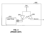
- FIG. 2 schematically shows a transmitter 200 of an optical transceiver that includes a laser diode driver 210 that drives a laser diode 220 , the output signal of which is monitored by a photodiode 230 .
- the photodiode 230 produces a current (I MONITOR ) in proportion to the amount of light emitted by laser diode 220 .
- the transceiver in each ONU 120 operates in a burst mode, i.e., the laser diode 220 outputs optical signals only during assigned time slots.
- the laser diode transmits two logic levels corresponding to logic “high” and logic “low”.
- the power level of the laser signal varies according to whether logic “high” or logic “low” signals are transmitted. Even when the laser diode is OFF, some residual power is transmitted by the laser diode and so its power level is not exactly zero.
- Two values are used to control the power level of the output optical signal: average power (AP) and extinction ratio (ER).
- the AP is the average power of light emitted by the laser diode 220 when high logic level and low logic level signals are transmitted during ON time.
- the ER is the ratio between light illuminated at “high” and “low” times. That is,
- the P ON Low and P ON High are the respective low logic level and high logic level optical power levels during ON time.
- One type of failure that causes an ONU 120 to always transmit data or noise to the common channel is know as “rogue ONU”. This may result from a laser diode 220 that has some radiant power during OFF time.
- techniques for detecting rogue ONU failures are based on measuring the AP and comparing the AP value to a predefined threshold. If that AP exceeds the threshold value, the laser diode 220 is shut down.
- An example for such technique is disclosed in U.S. Pat. No. 6,650,839 which is incorporated herein by reference for its useful background descriptions of the state of the art heretofore.
- the disadvantage of the detection of rogue ONU based on the AP is the substantial delay in generating an indication on such failures. This delay results from the time required for measuring the AP value, which is typically done using a low pass filter after the energy in the photodiode 230 is discharged.
- Another disadvantage of the AP based detection is the inability to determine the power levels of high and low levels at ON times, and to adjust these levels to achieve proper operation of the transmitter 200 .
- Safety standards demand that optical devices automatically detect such hazards in order to prevent eye injuries resulting from a laser diode transmitting high optical power. This may occur due to an electric short in the laser diode 220 or a disconnected photodiode 230 .
- the disclosed invention provides a circuit that allows fast and reliable detection of failures in passive optical networks (PONs).
- PONs passive optical networks
- the present invention detects rogue optical network unit (ONU) failures' based on the power levels during ON and OFF times rather than on the average power produced by a laser diode.
- ONU optical network unit
- eye-safety hazards that result from malfunctions in optical transceivers are detected.
- a power determination unit coupled to the photodiode for providing measurements of an output optical power of a high logic level and a low logic level of said digital burst data during ON times of the optical transmitter and for providing a measurement of an output optical power during OFF times of the optical transmitter;
- a logic unit coupled to the power determination unit and being responsive to said measurements for generating control and calibration signals.
- a power determination unit coupled to an output of a photodiode for providing a measurement of an output optical power during OFF time of the optical transmitter
- a logic unit coupled to the power determination unit and being responsive to generate a control signal for disabling the optical transmitter in a case of a rogue ONU failure.
- a power determination unit coupled to the photodiode for providing measurements of an output optical power of a high logic level and a low logic level of said digital burst data during ON times of the optical transmitter and for providing a measurement of an output optical power during OFF times of the optical transmitter;
- a logic unit coupled to the power determination unit and being responsive to said measurements for generating an indication signal indicative of one or more eye safety hazards.
- FIG. 1 is an exemplary diagram of a typical prior art PON
- FIG. 2 is an exemplary diagram of a prior art optical transmitter
- FIG. 3 is a schematic diagram of a circuit for measuring the output optical power level of a laser diode in accordance with the present invention
- FIGS. 4 a, b and c are a series of graphs showing the optical power during ON and OFF times
- FIG. 5 is a schematic diagram of a circuit for detecting rogue ONU failures in accordance with the present invention.
- FIG. 6 is a flowchart describing the method for detecting rogue ONU failures in accordance with the present invention.
- FIG. 7 is a schematic diagram of a circuit for eye safety hazards in accordance with the present invention.
- FIG. 3 shows an exemplary and non-limiting circuit 300 for measuring the output optical power level of a laser diode in accordance with the principles of the present invention.
- the circuit 300 includes a laser diode driver 310 , a laser diode 320 , a photodiode 330 , a switch 340 , and current amplifiers 350 and 360 .
- the laser diode driver 310 is coupled to the laser diode 320 and produces a bias current I BIAS and a modulation current I MOD .
- the bias current I BIAS is a continuous fixed current that is usually necessary to ensure proper dynamic performance of the laser diode 320 .
- the modulation current I MOD is superimposed on the bias current I BIAS during ON times for producing an optical signal that varies as a function of the modulation current I MOD .
- the laser diode 320 produces optical signals based on the I BIAS and I MOD provided by the laser diode driver 210 . Specifically, The I BIAS and I MOD current signals respectively determine the power level of the output signal during OFF and ON times.
- the laser diode 320 may be, but is not limited to, a Fabry-Perot (FP) laser, a distributed feedback (DFB) laser, and the likes.
- the photodiode 330 produces current (I MONITOR ) at an output 301 that is proportional to the amount of light emitted by the laser diode 320 .
- the switch 340 is coupled to an output 301 of the photodiode 330 and can be selectively coupled to either one of the current amplifiers 350 and 360 .
- the current amplifiers 350 and 360 sample the I MONITOR current at the input 301 and provide amplified output current signals.
- FIG. 4 a shows digital data that is transmitted during laser diode ON times shown in FIG. 4 b .
- FIG. 4 c shows laser optical power as a function of the measured current I MONITOR .
- the switch 340 is connected to the current amplifier 350 when data is transmitted and the laser diode 320 produces the optimal power. When data is not transmitted the switch 340 is toggled to the current amplifier 360 . As shown in FIG.
- the current amplifier 350 generates two current signals I High ON and I Low ON providing measurements of high logic and low logic levels of data transmitted during ON time (T 1 ).
- the current amplifier 360 generates a current signal I OFF of the optical power during OFF time (T 2 ).
- the current amplifiers 350 and 360 constitute a power determination unit that determines the power of the laser signal during OFF times and determines separately the power of the laser signal during ON times according to whether logic low or logic high signals are transmitted.
- the outputs 302 , 303 and 304 of the current amplifiers 350 and 360 respectively provide the measurements of I High ON and I Low ON and I OFF of the optical power during ON and OFF times. These measurements can be used for calibrating the output power of the laser diode 320 and detecting rogue ONU failures as well as eye safety hazards.
- a schematic diagram of a circuit 500 utilized for these purposes and constructed in accordance with an embodiment of the present invention is illustrated in FIG. 5 .
- the circuit 500 includes a laser diode driver 510 , a laser diode 520 , a photodiode 530 , a switch 540 and current amplifiers 550 and 560 having the same functionality as described above.
- the circuit 500 further includes a logic unit 570 , an adjustment unit 580 and a switch 590 .
- the logic unit 570 respectively receives, at inputs 501 and 502 , the measured I High ON and I Low ON current signals and, at an input 503 , the measured I OFF current and is responsive to the signals at these inputs for generating three respective signals “set ON power”, “set OFF power” and “shutdown”.
- the “set ON power” and “set OFF power” signals constitute calibration signals that define the difference between the measured power and a predefined value and allow for calibrating the output optical power of the laser diode 520 .
- the “shutdown” signal constitutes a control signal that controls the switch 590 and enables the laser diode 520 to be disconnected from the power supply if a rogue ONU failure is detected.
- the logic unit 570 includes comparators 572 , 574 and 576 coupled to respective outputs of the current amplifiers 550 and 560 .
- the comparator 572 compares between the current I High ON at the first output of the current amplifier 550 and a first threshold (TH 1 ). If the I High ON current is greater than the value of TH 1 , the comparator 572 outputs a high logic value; otherwise, a low logic value is generated.
- the first threshold determines the expected power level during ON times when high logic level signals are transmitted.
- the comparator 574 compares between the I Low ON current at the second output of the current amplifier 550 and a second threshold (TH 2 ). The second threshold determines the expected power level during ON times when low logic level signals are transmitted.
- the outputs of comparators 572 and 574 are the “set ON power” and “set OFF power” signals, respectively.
- the first and second thresholds can be defined according to the average power (AP) and extinction ratio (ER) values that provide the optimal performance of the laser diode 520 .
- the comparator 576 compares between the I OFF current at the output of the current amplifier 560 and a third threshold (TH 3 ), which defines the maximum allowed power level during OFF time. If the value of the I OFF current exceeds TH 3 the “shutdown” signal is asserted instructing the switch 590 to disconnect the laser diode 520 from the power supply.
- the shutdown signal can provide an indication of a rogue ONU failure.
- the adjustment unit 580 receives the “set ON power” and “set OFF power” signals and adjusts the I MOD and I BIAS currents of the laser diode driver 520 . Specifically, the “set ON power” and the “set off power” signals respectively control the I MOD current and I BIAS current. If the setting signal is a high logic value, the adjustment unit 580 increases the respective current signal; otherwise, the current is decreased. Each time that a setting signal is asserted the current is changed by an interval determined by the adjustment unit 580 . In order to rapidly equalize the measured power levels to the thresholds, the size of the current interval is reduced over time. The calibration of the I MOD and I BIAS is performed during the operation of the laser diode 520 .
- the adjustment unit 580 is a temperature dependent element ensuring the proper operation of the laser driver 510 and laser diode 520 over a wide range of temperatures.
- a temperature dependent element is coupled to a temperature compensation circuit, which adjusts the level of a current source of the element in response to the changes in the temperature.
- An example for a temperature compensation circuit may be found in U.S. patent application Ser. No. 11/512,237 titled “Method and circuit for providing a temperature dependent current source” filed Aug. 30, 2006 U.S. Pat. No. 7,288,983 assigned to the present assignee and whose contents are wholly incorporated herein by reference.
- FIG. 6 shows a non-limiting and exemplary flowchart 600 describing the process for detecting rogue ONU failures in accordance with an embodiment of the present invention.
- the method may be operated on the circuit 500 described in more detail above.
- the optical output power of a laser diode for example the laser diode 520
- a light sensitive device for example the photodiode 530
- the optical power output, or the light illuminated, by the laser diode is a function of at least the bias and modulation current.
- the monitor current the power level of the laser diode during OFF times I OFF is measured.
- the measured power I OFF is compared to a threshold signal I ROGUE that defines the maximum allowed power during OFF times of the laser diode. If the value of the I OFF signal is above the I ROGUE , then at S 640 a signal is asserted disconnecting the laser diode from the power supply.
- the circuit 300 can be integrated in an eye safety mechanism implemented in an ONU.
- two failures in an optical transmitter may cause eye safety hazards: 1) a laser diode constantly emits optical power; and 2) a photodiode is disconnected causing an internal laser power control to increase the optical power to a dangerous level.
- FIG. 7 shows an exemplary and non-limiting diagram of a circuit 700 utilized for detecting eye safety hazards according to the present invention.
- the circuit 700 is specifically designed to operate in conjunction with burst mode ONUs.
- the circuit 700 includes a laser driver 710 , a laser diode 720 and a photodiode 730 , having the same functionality as described above with reference to FIGS. 2 and 3 of the drawings.
- the output of the photodiode 730 is coupled to a power determination unit 740 that measures power levels (I High ON , I Low ON and I OFF ) of the laser diode 720 during ON and OFF times. This may be done as described above with reference to FIG. 3 .
- a logic unit 750 generates an eye safety indication based on the I High ON , I Low ON and I OFF signals.
- the logic unit 750 includes three comparators 752 , 754 , and 756 as well as an OR gate 758 .
- the comparator 752 checks whether the photodiode 730 is disconnected by comparing the I High ON current to a first threshold (TH 1 ) and if the I High ON current is less than the value TH 1 , the comparator 752 outputs a high logic value. The comparison is performed while data is transmitted, i.e., while a TX data signal (provided as an input to the logic unit 750 ) is asserted. The value of TH 1 determines the expected optical power when data is transmitted.
- the comparators 754 and 756 check whether the laser diode constantly produces optical power. With this aim, comparator 754 compares the I Low ON current to a second threshold (TH 2 ).
- the comparator 754 If during ON times the I Low ON current is greater than the value TH 2 , the comparator 754 outputs a high logic value.
- the comparator 756 compares the I OFF current to a third threshold (TH 3 ). If during OFF times the I OFF current exceeds the value of TH 3 , the comparator 756 asserts a high logic value.
- the value of TH 3 determines the expected optical power during off time, whereas TH 2 defines the expected optical power when data when low logic level signals are transmitted during ON time. All thresholds are programmable.
- the OR gate 758 receives the outputs of the comparators 752 , 754 and 756 and asserts an eye safety indication if at least one of the outputs has a high logic value.
- the eye safety indication may be utilized to disconnect the laser diode 720 from the power supply, for example, by means of a switch 760 .
- the circuit 700 may include a timer adapted to generate an alarm if none of the above checks were performed during a predefined time interval.
- the current amplifiers 350 and 360 are employed to determine the power of the laser signal during OFF times and to determine separately the power of the laser signal during ON times according to whether logic low or logic high signals are transmitted, other forms of power determination unit may also be used.
- the power determination unit may employ an operational amplifier (Op-Amp) that is configured to operate as an integrator, a sample and hold circuit, a buffer, and the likes.
- Op-Amp operational amplifier
Landscapes
- Engineering & Computer Science (AREA)
- Computer Networks & Wireless Communication (AREA)
- Physics & Mathematics (AREA)
- Electromagnetism (AREA)
- Signal Processing (AREA)
- Semiconductor Lasers (AREA)
- Optical Communication System (AREA)
Abstract
Description
| U.S. Pat. No. 6,650,839 | November 2003 | Mallard, Jr., et al. | ||
| U.S. Pat. No. 6,115,163 | September 2000 | Nobuhara | ||
| U.S. Pat. No. 6,108,112 | August 2000 | Touma | ||
| U.S. 20020076143 | June 2002 | Foltzer | ||
Claims (32)
Priority Applications (1)
| Application Number | Priority Date | Filing Date | Title |
|---|---|---|---|
| US11/514,937 US7646990B2 (en) | 2006-09-05 | 2006-09-05 | Circuit for detecting optical failures in a passive optical network |
Applications Claiming Priority (1)
| Application Number | Priority Date | Filing Date | Title |
|---|---|---|---|
| US11/514,937 US7646990B2 (en) | 2006-09-05 | 2006-09-05 | Circuit for detecting optical failures in a passive optical network |
Publications (2)
| Publication Number | Publication Date |
|---|---|
| US20080056731A1 US20080056731A1 (en) | 2008-03-06 |
| US7646990B2 true US7646990B2 (en) | 2010-01-12 |
Family
ID=39151688
Family Applications (1)
| Application Number | Title | Priority Date | Filing Date |
|---|---|---|---|
| US11/514,937 Expired - Fee Related US7646990B2 (en) | 2006-09-05 | 2006-09-05 | Circuit for detecting optical failures in a passive optical network |
Country Status (1)
| Country | Link |
|---|---|
| US (1) | US7646990B2 (en) |
Cited By (8)
| Publication number | Priority date | Publication date | Assignee | Title |
|---|---|---|---|---|
| US20100067901A1 (en) * | 2008-09-12 | 2010-03-18 | Masahiko Mizutani | Passive optical network system and fault determination method |
| US20100272433A1 (en) * | 2009-04-22 | 2010-10-28 | Futurewei Technologies, Inc. | Method for Identifying the Optical Network Unit Power Off Reason |
| US20110286566A1 (en) * | 2010-05-24 | 2011-11-24 | Kabushiki Kaisha Toshiba | Nuclear reactor oscillation power range monitor, and method and program therefor |
| US20120039602A1 (en) * | 2010-08-13 | 2012-02-16 | David Hood | Method and Apparatus for Detecting Rogue Optical Network Unit in Passive Optical Network |
| US20120224864A1 (en) * | 2009-11-18 | 2012-09-06 | Joachim Walewski | Method and arrangement for stabilizing a color coding method and optically transferring data |
| US20130336650A1 (en) * | 2012-06-19 | 2013-12-19 | Mohammad Azadeh | Enhanced Received Signal Power Indicators for Optical Receivers and Transceivers, and Methods of Making and Using the Same |
| US9407358B2 (en) * | 2014-08-19 | 2016-08-02 | Ubiquoss Inc. | Optical network terminal with functions of detecting and recovering from failures, blocking supplied power, and storing information, and method of detecting continuous optical output using the same |
| US20230246713A1 (en) * | 2022-02-01 | 2023-08-03 | Prime World International Holdings Ltd. | Optical communication system capable of ensuring operation safety of external laser source |
Families Citing this family (15)
| Publication number | Priority date | Publication date | Assignee | Title |
|---|---|---|---|---|
| US9479255B2 (en) * | 2008-04-30 | 2016-10-25 | Arris Enterprises, Inc. | Method and apparatus for controlling the optical output power from a burst mode laser |
| WO2009152834A1 (en) * | 2008-06-19 | 2009-12-23 | Telefonaktiebolaget Lm Ericsson (Publ) | Transmitter disabling device |
| CN101729938B (en) * | 2008-10-21 | 2013-03-20 | 华为技术有限公司 | Method, device and system for eliminating interference in passive optical network system |
| TWI387227B (en) * | 2009-02-20 | 2013-02-21 | Delta Electronics Inc | Optical network unit and abnormal detecting & power monitoring method thereof |
| CN101710847A (en) * | 2009-12-09 | 2010-05-19 | 中兴通讯股份有限公司 | Failure detection and control method of optical network unit and optical network unit |
| CN101789824A (en) * | 2009-12-30 | 2010-07-28 | 中兴通讯股份有限公司 | Online optical network unit (ONU) optical power acquisition device and method |
| CN101834666A (en) * | 2010-05-07 | 2010-09-15 | 成都优博创技术有限公司 | Device and method for testing burst optical power of optical network unit |
| CN101969343B (en) * | 2010-08-26 | 2013-08-14 | 成都优博创技术有限公司 | Method and device for abnormal continuous luminous detection, report and turn-off |
| WO2012139516A1 (en) * | 2011-04-13 | 2012-10-18 | Zte Corporation | Mitigating rogue optical network unit (onu) behavior in a passive optical network (pon) |
| CN102938671B (en) * | 2012-09-26 | 2015-08-12 | 青岛海信宽带多媒体技术有限公司 | Terminal equipment and long luminescence detection circuit thereof |
| US10033459B2 (en) * | 2013-02-15 | 2018-07-24 | Lantiq Deutschland Gmbh | System, method and apparatus for a rogue optics network unit |
| CN103269248A (en) * | 2013-05-06 | 2013-08-28 | 上海斐讯数据通信技术有限公司 | Device and method for detecting long-lasting illumination of terminal equipment |
| EP3005594A1 (en) * | 2013-06-04 | 2016-04-13 | Telefonaktiebolaget LM Ericsson (publ) | Transceiver for use in fibre network |
| WO2014205840A1 (en) * | 2013-06-29 | 2014-12-31 | 华为技术有限公司 | Optical signal monitoring method, signal monitoring device and optical network system |
| CN115633275B (en) * | 2022-11-16 | 2023-12-01 | 厦门优迅高速芯片有限公司 | ONU (optical network Unit) burst luminescence detection data processing method and related equipment |
Citations (6)
| Publication number | Priority date | Publication date | Assignee | Title |
|---|---|---|---|---|
| US6108112A (en) | 1997-03-19 | 2000-08-22 | Fujitsu Limited | Method and apparatus for failure recovery in passive optical network |
| US6115163A (en) | 1997-10-07 | 2000-09-05 | Fujitsu Limited | Apparatus and method for reception of optical burst |
| US20020076143A1 (en) | 2000-12-15 | 2002-06-20 | Alcatel Usa Sourcing, L.P. | Multi-channel, multi-mode redundant optical local loop having a bus topology |
| US20020097471A1 (en) * | 2001-01-22 | 2002-07-25 | Bethea Clyde George | Data transmission via direct modulation of a mid-IR laser |
| US6650839B1 (en) | 2000-05-23 | 2003-11-18 | Quantum Bridge Communications, Inc. | Method and apparatus for optical media access protection in a passive optical network |
| US7505692B2 (en) * | 2004-08-31 | 2009-03-17 | Cisco Technology, Inc. | System and method for optical transmission |
-
2006
- 2006-09-05 US US11/514,937 patent/US7646990B2/en not_active Expired - Fee Related
Patent Citations (6)
| Publication number | Priority date | Publication date | Assignee | Title |
|---|---|---|---|---|
| US6108112A (en) | 1997-03-19 | 2000-08-22 | Fujitsu Limited | Method and apparatus for failure recovery in passive optical network |
| US6115163A (en) | 1997-10-07 | 2000-09-05 | Fujitsu Limited | Apparatus and method for reception of optical burst |
| US6650839B1 (en) | 2000-05-23 | 2003-11-18 | Quantum Bridge Communications, Inc. | Method and apparatus for optical media access protection in a passive optical network |
| US20020076143A1 (en) | 2000-12-15 | 2002-06-20 | Alcatel Usa Sourcing, L.P. | Multi-channel, multi-mode redundant optical local loop having a bus topology |
| US20020097471A1 (en) * | 2001-01-22 | 2002-07-25 | Bethea Clyde George | Data transmission via direct modulation of a mid-IR laser |
| US7505692B2 (en) * | 2004-08-31 | 2009-03-17 | Cisco Technology, Inc. | System and method for optical transmission |
Non-Patent Citations (1)
| Title |
|---|
| U.S. Appl. No. 11/512,237, filed Aug. 30, 2006, Schwartsglass et al. |
Cited By (17)
| Publication number | Priority date | Publication date | Assignee | Title |
|---|---|---|---|---|
| US8254780B2 (en) * | 2008-09-12 | 2012-08-28 | Hitachi, Ltd. | Passive optical network system and fault determination method |
| US20100067901A1 (en) * | 2008-09-12 | 2010-03-18 | Masahiko Mizutani | Passive optical network system and fault determination method |
| US8787751B2 (en) * | 2009-04-22 | 2014-07-22 | Futurewei Technologies, Inc. | Method for identifying the optical network unit power off reason |
| US20100272433A1 (en) * | 2009-04-22 | 2010-10-28 | Futurewei Technologies, Inc. | Method for Identifying the Optical Network Unit Power Off Reason |
| US9432114B2 (en) * | 2009-04-22 | 2016-08-30 | Futurewei Technologies, Inc. | Method for identifying the optical network unit power off reason |
| US20140233941A1 (en) * | 2009-04-22 | 2014-08-21 | Futurewei Technologies, Inc. | Method for Identifying the Optical Network Unit Power Off Reason |
| US8811825B2 (en) * | 2009-11-18 | 2014-08-19 | Siemens Aktiengesellschaft | Method and arrangement for stabilizing a color coding method and optically transferring data |
| US20120224864A1 (en) * | 2009-11-18 | 2012-09-06 | Joachim Walewski | Method and arrangement for stabilizing a color coding method and optically transferring data |
| US20110286566A1 (en) * | 2010-05-24 | 2011-11-24 | Kabushiki Kaisha Toshiba | Nuclear reactor oscillation power range monitor, and method and program therefor |
| US9595356B2 (en) * | 2010-05-24 | 2017-03-14 | Kabushiki Kaisha Toshiba | Nuclear reactor oscillation power range monitor, and method and program therefor |
| US20120039602A1 (en) * | 2010-08-13 | 2012-02-16 | David Hood | Method and Apparatus for Detecting Rogue Optical Network Unit in Passive Optical Network |
| US8842990B2 (en) * | 2010-08-13 | 2014-09-23 | Telefonaktiebolaget L M Ericsson (Publ) | Method and apparatus for detecting rogue optical network unit in passive optical network |
| US20130336650A1 (en) * | 2012-06-19 | 2013-12-19 | Mohammad Azadeh | Enhanced Received Signal Power Indicators for Optical Receivers and Transceivers, and Methods of Making and Using the Same |
| US8901474B2 (en) * | 2012-06-19 | 2014-12-02 | Source Photonics, Inc. | Enhanced received signal power indicators for optical receivers and transceivers, and methods of making and using the same |
| US9407358B2 (en) * | 2014-08-19 | 2016-08-02 | Ubiquoss Inc. | Optical network terminal with functions of detecting and recovering from failures, blocking supplied power, and storing information, and method of detecting continuous optical output using the same |
| US20230246713A1 (en) * | 2022-02-01 | 2023-08-03 | Prime World International Holdings Ltd. | Optical communication system capable of ensuring operation safety of external laser source |
| US11784715B2 (en) * | 2022-02-01 | 2023-10-10 | Prime World International Holdings Ltd. | Optical communication system capable of ensuring operation safety of external laser source |
Also Published As
| Publication number | Publication date |
|---|---|
| US20080056731A1 (en) | 2008-03-06 |
Similar Documents
| Publication | Publication Date | Title |
|---|---|---|
| US7646990B2 (en) | Circuit for detecting optical failures in a passive optical network | |
| US8208814B2 (en) | Optical transceiver calibration system and method | |
| CA2607364C (en) | Method and apparatus for controlling a semiconductor optical amplifier for use in a passive optical network | |
| US9755750B2 (en) | Mitigating noise and OBI in RFoG networks | |
| US7483455B2 (en) | Control method and control circuit for laser diode, and optical transmitter using the same | |
| US7504610B2 (en) | Optical modulation amplitude compensation system having a laser driver with modulation control signals | |
| US20070116466A1 (en) | Optical network unit (ONU) circuit | |
| US6369926B1 (en) | Multichannel light source wavelength and strength stabilizing apparatus and method thereof | |
| US4553268A (en) | Circuit arrangement with a laser diode for transmission of communication signals through a light waveguide | |
| US6980742B1 (en) | Wavelength control in optical WDM systems | |
| US8588609B2 (en) | Wavelength division multiplexing transmission system and apparatus and optical signal noise ratio calculation method | |
| US20050201761A1 (en) | SINGLE FIBER TRANSCEIVER with FAULT LOCALIZATION | |
| CN101258576A (en) | In-situ power monitor having an extended range to stabilize gain of avalanche photodiodes across temperature variations | |
| US8983308B2 (en) | Optical network device with multi-transport support | |
| US20130028598A1 (en) | Optical networks | |
| US11070295B2 (en) | PON system, optical network unit, optical line terminal, method of registering optical network unit, and data structure | |
| EP1324516B1 (en) | Apparatus for detecting cross-talk and method therefor | |
| US20210083778A1 (en) | Optical communication apparatus, wavelength calibration method, and program | |
| US20100129079A1 (en) | Optical wdm transmission apparatus and optical wdm transmission method | |
| JP4531098B2 (en) | Optical communication system | |
| US20050031357A1 (en) | Controlling the extinction ratio in optical networks | |
| US6490080B2 (en) | Gain controlled optically pre-amplified receiver apparatus and method | |
| US20080080871A1 (en) | Slice level control | |
| US6919963B2 (en) | Apparatus for detecting wavelength drift and method therefor | |
| WO2011024350A1 (en) | Light-emission error preventing circuit for optical transmitter |
Legal Events
| Date | Code | Title | Description |
|---|---|---|---|
| AS | Assignment |
Owner name: BROADLIGHT LTD., ISRAEL Free format text: ASSIGNMENT OF ASSIGNORS INTEREST;ASSIGNORS:WEBER, RAVIV;KOREN, ASAF;REEL/FRAME:018270/0391;SIGNING DATES FROM 20060831 TO 20060904 |
|
| AS | Assignment |
Owner name: PLENUS II (D.C.M.), LIMITED PARTNERSHIP, ISRAEL Free format text: SECURITY AGREEMENT;ASSIGNOR:BROADLIGHT LTD.;REEL/FRAME:018981/0325 Effective date: 20070214 Owner name: PLENUS II, LIMITED PARTNERSHIP, ISRAEL Free format text: SECURITY AGREEMENT;ASSIGNOR:BROADLIGHT LTD.;REEL/FRAME:018981/0325 Effective date: 20070214 |
|
| STCF | Information on status: patent grant |
Free format text: PATENTED CASE |
|
| AS | Assignment |
Owner name: BROADLIGHT LTD., ISRAEL Free format text: RELEASE BY SECURED PARTY;ASSIGNORS:PLENUS II, LIMITED PARTNERSHIP;PLENUS II (D.C.M.), LIMITED PARTNERSHIP;REEL/FRAME:023741/0609 Effective date: 20091220 |
|
| AS | Assignment |
Owner name: BROADCOM INTERNATIONAL LIMITED, CAYMAN ISLANDS Free format text: ASSIGNMENT OF ASSIGNORS INTEREST;ASSIGNOR:BROADCOM BROADBAND ACESS LTD.;REEL/FRAME:029256/0895 Effective date: 20120601 Owner name: BROADCOM CORPORATION, CALIFORNIA Free format text: ASSIGNMENT OF ASSIGNORS INTEREST;ASSIGNOR:BROADCOM INTERNATIONAL LIMITED;REEL/FRAME:029256/0939 Effective date: 20120601 Owner name: BROADCOM BROADBAND ACCESS LTD., ISRAEL Free format text: CHANGE OF NAME;ASSIGNOR:BROADLIGHT LTD.;REEL/FRAME:029259/0975 Effective date: 20120624 |
|
| FPAY | Fee payment |
Year of fee payment: 4 |
|
| FEPP | Fee payment procedure |
Free format text: PAT HOLDER NO LONGER CLAIMS SMALL ENTITY STATUS, ENTITY STATUS SET TO UNDISCOUNTED (ORIGINAL EVENT CODE: STOL); ENTITY STATUS OF PATENT OWNER: LARGE ENTITY |
|
| AS | Assignment |
Owner name: BANK OF AMERICA, N.A., AS COLLATERAL AGENT, NORTH CAROLINA Free format text: PATENT SECURITY AGREEMENT;ASSIGNOR:BROADCOM CORPORATION;REEL/FRAME:037806/0001 Effective date: 20160201 Owner name: BANK OF AMERICA, N.A., AS COLLATERAL AGENT, NORTH Free format text: PATENT SECURITY AGREEMENT;ASSIGNOR:BROADCOM CORPORATION;REEL/FRAME:037806/0001 Effective date: 20160201 |
|
| AS | Assignment |
Owner name: AVAGO TECHNOLOGIES GENERAL IP (SINGAPORE) PTE. LTD., SINGAPORE Free format text: ASSIGNMENT OF ASSIGNORS INTEREST;ASSIGNOR:BROADCOM CORPORATION;REEL/FRAME:041706/0001 Effective date: 20170120 Owner name: AVAGO TECHNOLOGIES GENERAL IP (SINGAPORE) PTE. LTD Free format text: ASSIGNMENT OF ASSIGNORS INTEREST;ASSIGNOR:BROADCOM CORPORATION;REEL/FRAME:041706/0001 Effective date: 20170120 |
|
| AS | Assignment |
Owner name: BROADCOM CORPORATION, CALIFORNIA Free format text: TERMINATION AND RELEASE OF SECURITY INTEREST IN PATENTS;ASSIGNOR:BANK OF AMERICA, N.A., AS COLLATERAL AGENT;REEL/FRAME:041712/0001 Effective date: 20170119 |
|
| FPAY | Fee payment |
Year of fee payment: 8 |
|
| AS | Assignment |
Owner name: AVAGO TECHNOLOGIES INTERNATIONAL SALES PTE. LIMITE Free format text: MERGER;ASSIGNOR:AVAGO TECHNOLOGIES GENERAL IP (SINGAPORE) PTE. LTD.;REEL/FRAME:047195/0827 Effective date: 20180509 |
|
| AS | Assignment |
Owner name: AVAGO TECHNOLOGIES INTERNATIONAL SALES PTE. LIMITE Free format text: CORRECTIVE ASSIGNMENT TO CORRECT THE EFFECTIVE DATE OF MERGER PREVIOUSLY RECORDED AT REEL: 047195 FRAME: 0827. ASSIGNOR(S) HEREBY CONFIRMS THE MERGER;ASSIGNOR:AVAGO TECHNOLOGIES GENERAL IP (SINGAPORE) PTE. LTD.;REEL/FRAME:047924/0571 Effective date: 20180905 |
|
| FEPP | Fee payment procedure |
Free format text: MAINTENANCE FEE REMINDER MAILED (ORIGINAL EVENT CODE: REM.); ENTITY STATUS OF PATENT OWNER: LARGE ENTITY |
|
| LAPS | Lapse for failure to pay maintenance fees |
Free format text: PATENT EXPIRED FOR FAILURE TO PAY MAINTENANCE FEES (ORIGINAL EVENT CODE: EXP.); ENTITY STATUS OF PATENT OWNER: LARGE ENTITY |
|
| STCH | Information on status: patent discontinuation |
Free format text: PATENT EXPIRED DUE TO NONPAYMENT OF MAINTENANCE FEES UNDER 37 CFR 1.362 |
|
| FP | Lapsed due to failure to pay maintenance fee |
Effective date: 20220112 |