US7522848B2 - Receiver with dynamically adjustable decision threshold voltage based on input power - Google Patents
Receiver with dynamically adjustable decision threshold voltage based on input power Download PDFInfo
- Publication number
- US7522848B2 US7522848B2 US10/955,575 US95557504A US7522848B2 US 7522848 B2 US7522848 B2 US 7522848B2 US 95557504 A US95557504 A US 95557504A US 7522848 B2 US7522848 B2 US 7522848B2
- Authority
- US
- United States
- Prior art keywords
- optical signal
- voltage
- set point
- threshold voltage
- logical
- Prior art date
- Legal status (The legal status is an assumption and is not a legal conclusion. Google has not performed a legal analysis and makes no representation as to the accuracy of the status listed.)
- Active, expires
Links
Images


Classifications
-
- H—ELECTRICITY
- H03—ELECTRONIC CIRCUITRY
- H03K—PULSE TECHNIQUE
- H03K5/00—Manipulating of pulses not covered by one of the other main groups of this subclass
- H03K5/01—Shaping pulses
- H03K5/08—Shaping pulses by limiting; by thresholding; by slicing, i.e. combined limiting and thresholding
- H03K5/082—Shaping pulses by limiting; by thresholding; by slicing, i.e. combined limiting and thresholding with an adaptive threshold
-
- H—ELECTRICITY
- H03—ELECTRONIC CIRCUITRY
- H03F—AMPLIFIERS
- H03F1/00—Details of amplifiers with only discharge tubes, only semiconductor devices or only unspecified devices as amplifying elements
- H03F1/02—Modifications of amplifiers to raise the efficiency, e.g. gliding Class A stages, use of an auxiliary oscillation
- H03F1/0205—Modifications of amplifiers to raise the efficiency, e.g. gliding Class A stages, use of an auxiliary oscillation in transistor amplifiers
-
- H—ELECTRICITY
- H03—ELECTRONIC CIRCUITRY
- H03F—AMPLIFIERS
- H03F1/00—Details of amplifiers with only discharge tubes, only semiconductor devices or only unspecified devices as amplifying elements
- H03F1/08—Modifications of amplifiers to reduce detrimental influences of internal impedances of amplifying elements
-
- H—ELECTRICITY
- H03—ELECTRONIC CIRCUITRY
- H03F—AMPLIFIERS
- H03F3/00—Amplifiers with only discharge tubes or only semiconductor devices as amplifying elements
- H03F3/20—Power amplifiers, e.g. Class B amplifiers, Class C amplifiers
- H03F3/24—Power amplifiers, e.g. Class B amplifiers, Class C amplifiers of transmitter output stages
-
- H—ELECTRICITY
- H04—ELECTRIC COMMUNICATION TECHNIQUE
- H04B—TRANSMISSION
- H04B10/00—Transmission systems employing electromagnetic waves other than radio-waves, e.g. infrared, visible or ultraviolet light, or employing corpuscular radiation, e.g. quantum communication
- H04B10/60—Receivers
- H04B10/66—Non-coherent receivers, e.g. using direct detection
- H04B10/69—Electrical arrangements in the receiver
- H04B10/695—Arrangements for optimizing the decision element in the receiver, e.g. by using automatic threshold control
-
- H—ELECTRICITY
- H03—ELECTRONIC CIRCUITRY
- H03F—AMPLIFIERS
- H03F2200/00—Indexing scheme relating to amplifiers
- H03F2200/465—Power sensing
Definitions
- Embodiments of the present invention relate to telecommunication equipment and, in particular, to receivers.
- Receivers may be used in telecommunication systems and/or networks to receive data and/or other information on optical and/or electrical signals.
- Traditional receivers have limitations, however.
- FIG. 1 is a schematic diagram of a receiver according to an embodiment of the present invention
- FIG. 2 is a flow chart illustrating an approach to operating a receiver according to an embodiment of the present invention
- FIG. 3 is a graphical representation (or eye pattern) of a voltage signal according to an embodiment of the present invention.
- FIG. 4 is a graphical representation (or eye pattern) of a voltage signal according to an alternative embodiment of the present invention.
- FIG. 5 is a schematic diagram of a decision circuit according to an embodiment of the present invention.
- FIG. 6 is a high-level block diagram of a transponder or transceiver according to an embodiment of the present invention.
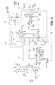
- FIG. 1 is a schematic diagram of a receiver 100 according to an embodiment of the present invention.
- the receiver 100 receives an optical signal 101 having a data stream thereon at a photodetector 102 , such as an avalanche photodiode or a positive-intrinsic-negative (PIN) diode, for example.
- the photodetector 102 is coupled to a transimpedance amplifier 104 (TIA 104 ), which is coupled to a decision amplifier 106 , such as a limiting amplifier, for example, via a capacitor 105 , such as a 0.1 pF capacitor, for example.
- the example decision amplifier 106 is coupled to a clock and data recovery (CDR) circuit 108 .
- CDR clock and data recovery
- the photodetector 102 also is coupled to a current sense circuit, such as a difference amplifier or differential amplifier 110 , via a resistor 112 .
- the illustrated differential amplifier 110 is coupled to a multiplier 114 , which is coupled to a level-shifting amplifier 116 (level shifter 116 ).
- the illustrated level shifter 116 is coupled to the decision amplifier 106 through a resistor 118 .
- a connector 120 such as a 300-pin multi-source agreement (MSA) connector, an XFP connector, a XENPAK connector, or other suitable connector, for example, is coupled to an analog-to-digital converter 122 (ADC 122 ), such as an ADC with twelve-bit resolution, for example.
- the ADC 122 is coupled to a microcontroller 124 , such as a precision mixed signal microcontroller, for example, is coupled to the multiplier 114 via a serial communication port.
- An analog threshold voltage value 131 may be input to the decision circuit 126 through a pin 137 and may be used as a set point to determine whether a data bit on an optical signal is a logical one or a logical zero.
- a digital threshold value 133 may be input to the decision circuit 126 through one or more pins 139 and may be used as the set point to determine whether a data bit on an optical signal is a logical one or a logical zero.
- the decision amplifier 106 , the differential amplifier 110 , the resistor 112 , the multiplier 114 , the level shifter 116 , the resistor 118 , the ADC 122 , and the microcontroller 124 may form a decision circuit 126 which may be used to dynamically adjust and/or scale the threshold voltage 140 based on dynamic variations in the incoming optical signal 101 power.
- the decision circuit 126 may be an analog circuit and thus the ADC 122 , microcontroller 124 may not be included, and the multiplier 114 may be an analog multiplier.
- the connector 120 may include a pin 137 to receive the set point 134 represented as an analog voltage 131 and/or one or more pins 139 to receive the set point 134 as a digital representation 133 via a digital serial communication link.
- FIG. 2 is a flow chart illustrating a process 200 for operating the receiver 100 according to an embodiment of the present invention in which the receiver 100 may dynamically adjust and/or scale the threshold voltage 140 based on the power in the incoming optical signal 101 .
- the process 200 begins with a block 202 , where control passes to a block 204 .
- the ADC 122 may receive an analog voltage 131 representing the threshold set point value 134 via the pin 137 on the connector 120 , converts the analog value to a digital value, and couples the digital value to the microcontroller 124 .
- a digital representation 133 of the set point 134 may be coupled to the microcontroller 124 through 120 .
- the set point 131 / 133 may be coupled to the mixer 114 .
- FIG. 3 is a graphical representation or eye pattern of an initial voltage signal 300 at the input to the decision amplifier 106 according to an embodiment of the present invention.
- the voltage signal has a value of one volt peak-to-peak (1.0Vpp)
- the eye pattern 300 includes the data bits acquired from the data stream overlaid on top of each other
- amplitude 304 is representative of a logic level one
- amplitude 306 representative of a logic level zero.
- the expected voltage signal 300 includes noise 308 on the logic level one and noise 310 on the logic level zero.
- the noise 308 and 310 may be optical noise and the amplitude of the noise 308 on the logic level one may be greater than the amplitude of the noise 310 on the logic level zero.
- a threshold voltage value 314 may be set below the midpoint between the logic one and zero levels to reduce the bit error rate of the receiver 100 .
- a user may measure the link bit error rate (BER) using forward error correction (FEC) circuitry (not shown) following the CDR 108 and then may modify the set point 134 by modifying the analog voltage 131 and/or digital representation 133 to reduce the BER in the recovered data stream. This may be accomplished at the beginning of life of the receiver 100 or by a user after the receiver 100 has been put into service, for example.
- FEC forward error correction
- the threshold voltage value 314 is ⁇ 0.25 volts or twenty-five percent (25%) of the expected signal amplitude and zero volts 312 represents fifty percent (50%) of the expected signal amplitude.
- the receiver 100 may determine that if the voltage level is ⁇ 0.25 volts or greater, then the data bit on the incoming optical signal 101 is a logical one.
- the receiver 100 may determine that if the voltage level is less than ⁇ 0.25 volts, then the data bit on the incoming optical signal 101 is a logical zero.
- the microcontroller 124 may receive the analog voltage 131 and/or digital representation 133 of the set point and couples the set point 134 to the multiplier 114 , via a serial communication port, for example.
- an optical fiber may couple an optical signal to the photodetector 102 , which may convert the optical signal 101 to a current 128 / 129 proportional to power of the optical signal 101 .
- the TIA 104 may receive the current 129 and convert it to a voltage signal proportional to the current 129 and the power of the optical signal 101 .
- the output of the TIA 104 may be a differential voltage signal 130 coupled to the decision amplifier 106 via the capacitor 105 .
- the capacitor 105 may ensure that the decision amplifier 106 and the level shifter 116 do not interfere with the direct current (DC) operating point of the TIA 104 .
- FIG. 4 is a graphical representation of an eye pattern representing a subsequently received voltage signal 400 at the input of the decision amplifier 106 from which a threshold voltage value 414 is produced according to an embodiment of the present invention.
- the voltage signal 400 has a value of 0.1 volts peak-to-peak (0.1Vpp)
- the eye pattern of the voltage signal 400 includes the data bits acquired from the data stream in the incoming optical signal 101 overlaid on top of each other
- amplitude 404 is representative of a logic level one
- amplitude 406 representative of a logic level zero.
- the voltage signal 400 includes noise 408 on the logic level one and noise 410 on the logic level zero.
- the noise 408 and 410 may be optical noise and the amplitude of the noise 408 on the logic level one may be greater than the amplitude of the noise 410 on the logic level zero.
- the adjusted threshold voltage value 414 may provide similar BER results for the voltage signal 400 as the threshold voltage value 314 provided for the voltage signal 300 .
- the differential amplifier 110 may measure the current 128 through the resistor 112 by sensing the voltage across the resistor 112 and the differential amplifier 110 outputs a voltage 132 , which may be proportional to the average power in the optical signal 101 , to the multiplier 114 .
- the differential amplifier 110 may amplify the difference between the signals on its non-inverting input and its inverting input.
- the multiplier 114 may scale the set point 134 based on the voltage 132 .
- the multiplier 114 may scale the set point 134 in proportion to the voltage 132 and average power in the optical signal 101 and provide a bipolar voltage 136 .
- the multiplier may multiply the voltage 132 times the set point 134 to obtain the bipolar voltage 136 .
- the bipolar voltage 136 in which zero volts represents fifty percent (50%) of the signal amplitude of the set point 134 may be coupled to the level shifter 116 .
- the level shifter 116 may shift the DC level of the bipolar voltage 136 to a level appropriate for operation of the decision amplifier 106 .
- the level shifter may sum the bipolar voltage 136 with a fixed positive voltage (not shown) to provide a level-shifted voltage 138 , which may be compatible with the DC operating point of the decision amplifier 106 .
- the level-shifted voltage 138 and a complementary voltage generated from the level-shifted voltage 138 may be buffered and summed into the differential data path prior to the input of the decision amplifier 106 as a voltage 140 .
- the capacitor 105 may provide alternating current (AC) coupling for the data signal path from the TIA 104 .
- the decision amplifier 106 may determine a logical one value and a logical zero value based on the voltage 138 , which represents the adjusted set point.
- the decision amplifier 106 may receive the voltage signal 130 of 1Vpp summed with the level-shifted voltage 138 and using the set point 134 of 25% of the peak-to-peak input voltage the receiver 100 may determine that if the voltage level is ⁇ 0.25 volts or greater, then the data bit on the incoming optical signal 101 is a logical one.
- the receiver 100 may determine that if the voltage level is less than ⁇ 0.25 volts, then the data bit on the incoming optical signal 101 is a logical zero.
- the CDR 108 may recover a data clock from the voltage 140 and re-clock data from the decision amplifier 106 .
- process 200 has been described as multiple discrete blocks performed in turn in a manner that may be most helpful in understanding embodiments of the invention. However, the order in which they are described should not be construed to imply that these operations are necessarily order dependent or that the operations be performed in the order in which the blocks are presented. Of course, the process 200 is an example process and other processes may be used to implement embodiments of the present invention.
- a machine-accessible medium with machine-readable data thereon may be used to cause a machine, such as, for example, a processor to perform the method 200 .
- FIG. 5 is a schematic diagram of the decision circuit 126 according to an embodiment of the present invention.
- the decision circuit 126 includes an operational amplifier U 1 coupled to the multiplier 114 , the multiplier 114 is coupled to the level shifter 116 , and the level shifter 116 is coupled to the resistor 118 .
- the example multiplier 114 includes a multiplying DAC U 2 and an operational amplifier U 3 .
- the example level shifter 116 includes a first operational amplifier U 4 , a second operational amplifier U 5 , and an offset DAC 502 .
- the example resistor 118 includes the resistors R 19 (100 ⁇ ), R 20 (499 ⁇ ), R 21 (100 ⁇ ), and R 22 (499 ⁇ ).
- the input (V in ) to the operational amplifier U 1 is the voltage signal 132 and the outputs (V outP and V outN , respectively) of the operational amplifiers U 4 and U 5 are the voltage 138 .
- the illustrated decision circuit 126 operates as follows.
- V in may be input to amplifier U 1 via resistor R 1 (4.99K ⁇ ) and amplifier U 1 may amplify V in .
- the gain of amplifier U 1 may be set at around 2.5.
- Diode D 1 and transistor Q 1 and their associated circuitry resistors R 2 (20K ⁇ ), R 3 (15K ⁇ ), and R 4 (10K ⁇ ), and capacitors C 1 (1.00 nf) and C 2 (270 pf) may clamp the output of amplifier U 1 to 2.5 volts.
- Resistor R 5 (20 ⁇ ) and capacitor C 3 (0.1 ⁇ f) may provide filtered biasing for amplifier U 1 .
- the output of U 1 may be coupled to the multiplier U 2 , which may be a sixteen-bit digital-to-analog converter (DAC), for example, that uses the output of U 1 to set the output range of the multiplier U 2 .
- the multiplier U 2 may multiply the threshold voltage or set point 134 by V in .
- the microcontroller 124 (not shown) may be coupled to the DIN port of the multiplier U 2 to provide the multiplier U 2 with serial data having the set point 134 .
- a signal to synchronize input of the serial data is input on the LSYN pin of the multiplier U 2
- a clock signal that may clock serial data having the set point 134 into the multiplier U 2 is input on the SCLK pin of the multiplier 114
- a VF pin may be a feedback connection for the multiplier U 2 .
- the multiplier U 2 may be a 16-bit DAC, there may be 2 16 or approximately 65K possible levels for the set point 134 .
- V in may be applied to the reference port VREF of the multiplier U 2 via a resistor R 6 (10 ⁇ ) and a capacitor C 4 (1.00 nf).
- the output VOUT of the multiplier U 2 may be V in scaled by the set point 134 .
- Resistor R 8 (20 ⁇ ) and capacitor C 6 (0.1 ⁇ f) may provide filtered biasing for the multiplier U 2 .
- the output of the multiplier U 2 may be coupled to the unipolar to bipolar converter U 3 via a resistor R 7 (4.99 ⁇ ) and a capacitor C 5 (100 pf).
- the unipolar to bipolar converter U 3 may convert the unipolar signal from U 2 (such as a 0-2.5 volts, for example) to the bipolar signal 136 (such as ⁇ 2.5 volts to +2.5 volts, for example).
- Zero volts out of U 3 may represent fifty percent (50%) of the threshold range, and ⁇ 2.5 volts to +2.5 volts may correspond to zero percent (0%) and one hundred percent (100%), respectively, of the threshold range.
- Resistors R 9 (20 ⁇ ) and R 10 (20 ⁇ ), and capacitors C 7 (0.1 ⁇ f) and C 8 (0.1 ⁇ f) may provide filtered biasing for the unipolar to bipolar converter U 3 .
- the unipolar to bipolar converter U 3 may drive the signal 136 to the amplifier U 4 via the resistor R 11 (10K ⁇ ) and amplifier U 4 may level shift and boost the current drive of the signal 138 into the decision amplifier 106 (not shown) with the amplifier U 4 gain being set by R 11 (10K ⁇ ) and R 13 (10K ⁇ ).
- the output of the amplifier U 4 couples to the amplifier U 5 , which produces the complementary threshold voltage to drive the complementary input to the decision amplifier 106 (not shown).
- the amplifier U 4 may drive the amplifier U 5 via the resistor R 17 (10K ⁇ ).
- the amplifier U 5 may invert U 4 's output to obtain V outP for the differential signal 138 into the tap resistors R 19 (100 ⁇ ), R 20 (499 ⁇ ), R 21 (100 ⁇ ), and R 22 (499 ⁇ ).
- V outP and V outN may be the differential inputs to the decision amplifier 106 (not shown).
- capacitors C 13 and C 14 may be 0.1 ⁇ f, each for filtering the threshold voltage.
- the amplifier U 4 includes a second input coupled through the resistor R 14 (4.99K ⁇ ).
- the second input may be a signal from a digital-to-analog converter (DAC) 502 , which may generate a voltage to nullify voltage offsets.
- the DAC 502 may trim out circuit offsets to obtain a true percentage of the threshold voltage or set point 136 .
- the threshold voltage or set point 134 may be set to fifty percent (50%)
- various offsets in the receiver 100 circuits may affect the threshold voltage or set point 136 .
- the DAC 502 output compensate for the offsets to obtain a true percentage of the set point 136 .
- Capacitors C 9 (0.1 ⁇ f) and C 10 (0.1 ⁇ f) may provide filtered biasing and a filtered input for the amplifier U 2 .
- the amplifier U 5 includes a second input coupled through the resistor R 15 (4.99K ⁇ ), which may be a signal 504 from a +2.5V voltage reference.
- Resistor R 16 (60.4K ⁇ ) and capacitor C 11 (0.1 ⁇ f) may provide voltage division and filtering for the amplifier U 4 input.
- V in I avg *R t (1)
- V in is the input signal 132 to amplifier U 1
- I avg is the average current of the photodetector 102
- R t is the transimpedance of the differential amplifier 110
- V out,N [V offset *(1 +G 2 ) ⁇ V in *G 1 *(1 ⁇ 2* D s )* G 2 ]*G 3 (2)
- V offset is the input to U 4 from the offset DAC 502 at resistor R 14
- G 2 is the gain provided by U 4
- G 1 is the gain provided by U 1
- D s is a normalized threshold voltage value or set point and may be set by the user anywhere from 0 to 1 to within the resolution of the multiplier U 2 , for example
- G 3 is the gain of the taps R 19 , R 20 , R 21 , and R 22 into the decision amplifier 106
- V out,N [V offset *(1 +G 2 ) ⁇ V in *G 1 *(1 ⁇ 2* D
- FIG. 6 is a high-level block diagram of a transponder and/or transceiver 600 according to an embodiment of the present invention.
- data 601 , a clock 603 are input to a multiplexer 602 via the connector 120 .
- the data 601 may be sixteen synchronized data lines and the multiplexer 602 may be a sixteen-to-one multiplexer that may multiplex the sixteen data lines to a ten gigabit per second (10 Gbps) serial data stream 604 , which is coupled to a driver 606 .
- 10 Gbps ten gigabit per second
- the driver may boost the amplitude of the data stream 604 and a Mach-Zehnder modulator, such as a lithium niobate (LiNiO 2 ) Mach-Zehnder modulator, for example, may convert the amplified serial data stream 604 to an optical signal 610 using light from a continuous wave laser 612 , such as a temperature tuned external cavity laser, for example.
- a jitter filter 614 is coupled to the multiplexer 602 and may clean up a reference clock 616 used to clock the data 601 at the 10 Gbps data rate.
- the optical signal 610 may be launched into an optical fiber 618 .
- an optical fiber 619 receives an optical signal, such as the optical signal 101 , and couples it to the photodetector 102 and the TIA 104 , whose outputs are coupled to the decision circuit 126 .
- the analog voltage 131 and/or digital representation 133 of the set point may be input to the decision circuit 126 via the connector 120 .
- the output of the decision circuit 126 is coupled to the clock and data recovery circuit (CDR) 108 , which may recover the serial data stream 604 from the output of 126 .
- CDR clock and data recovery circuit
- a demultiplexer 620 may separate the clock 603 and separate the data 60 into sixteen data lines from the serial data stream 604 .
- Embodiments of the present invention may be implemented using hardware, software, or a combination thereof.
- the software may be stored on a machine-accessible medium.
- a machine-accessible medium includes any mechanism that may be adapted to store and/or transmit information in a form accessible by a machine (e.g., a computer, network device, personal digital assistant, manufacturing tool, any device with a set of one or more processors, etc.).
- a machine-accessible medium includes recordable and non-recordable media (e.g., read only memory (ROM), random access memory (RAM), magnetic disk storage media, optical storage media, flash memory devices, etc.), as recess as electrical, optical, acoustic, or other form of propagated signals (e.g., carrier waves, infrared signals, digital signals, etc.).
Abstract
Description
V in =I avg *R t (1)
where Vin is the
V out,N =[V offset*(1+G 2)−V in *G 1*(1−2*D s)*G 2 ]*G 3 (2)
where Voffset is the input to U4 from the offset
V outP=(V nom −V outN)*G 3 (3)
where Vnom is the nominal (midrange) value for VoutP and VoutN that may be chosen based on the DC operating parameters of the amplifiers U4 and U5 and the
Claims (14)
Priority Applications (1)
| Application Number | Priority Date | Filing Date | Title |
|---|---|---|---|
| US10/955,575 US7522848B2 (en) | 2004-09-30 | 2004-09-30 | Receiver with dynamically adjustable decision threshold voltage based on input power |
Applications Claiming Priority (1)
| Application Number | Priority Date | Filing Date | Title |
|---|---|---|---|
| US10/955,575 US7522848B2 (en) | 2004-09-30 | 2004-09-30 | Receiver with dynamically adjustable decision threshold voltage based on input power |
Publications (2)
| Publication Number | Publication Date |
|---|---|
| US20060067711A1 US20060067711A1 (en) | 2006-03-30 |
| US7522848B2 true US7522848B2 (en) | 2009-04-21 |
Family
ID=36099244
Family Applications (1)
| Application Number | Title | Priority Date | Filing Date |
|---|---|---|---|
| US10/955,575 Active 2026-12-23 US7522848B2 (en) | 2004-09-30 | 2004-09-30 | Receiver with dynamically adjustable decision threshold voltage based on input power |
Country Status (1)
| Country | Link |
|---|---|
| US (1) | US7522848B2 (en) |
Cited By (3)
| Publication number | Priority date | Publication date | Assignee | Title |
|---|---|---|---|---|
| US20060177229A1 (en) * | 2005-01-17 | 2006-08-10 | Siemens Aktiengesellschaft | Regenerating an optical data signal |
| US20070206964A1 (en) * | 2005-08-19 | 2007-09-06 | Korea Advanced Institute Of Science And Technology | Receiver having an apparatus for varying decision threshold level and an optical transmission system having the same |
| US20130216219A1 (en) * | 2012-02-22 | 2013-08-22 | Fujitsu Limited | Optical receiving device |
Families Citing this family (6)
| Publication number | Priority date | Publication date | Assignee | Title |
|---|---|---|---|---|
| KR100674087B1 (en) * | 2004-11-22 | 2007-01-24 | 한국전자통신연구원 | Clock signal generation apparatus and method using asymmetrical distortion of NRZ signal, and optical transmission and receiving system using its |
| US8145059B2 (en) * | 2008-02-28 | 2012-03-27 | Gtran Corporation | Circuit topologies for high speed, low cost optical transceiver components |
| CN101355389A (en) * | 2008-09-11 | 2009-01-28 | 中兴通讯股份有限公司 | Method for optimization regulation of receiver decision level and apparatus thereof |
| US8155536B2 (en) * | 2008-12-31 | 2012-04-10 | Intel Corporation | Optical transceiver IC |
| CN106253977B (en) * | 2016-08-22 | 2019-05-21 | 青岛海信宽带多媒体技术有限公司 | The method of adjustment and optical module of LOS alarm decision threshold |
| US10097266B2 (en) * | 2017-02-10 | 2018-10-09 | Futurewei Technologies, Inc. | Threshold adjustment compensation of asymmetrical optical noise |
Citations (7)
| Publication number | Priority date | Publication date | Assignee | Title |
|---|---|---|---|---|
| US6359715B1 (en) * | 1997-11-28 | 2002-03-19 | Kokusai Electric Co., Ltd. | Photoelectric conversion, method light receiving circuit, and optical communication system |
| US6459335B1 (en) * | 2000-09-29 | 2002-10-01 | Microchip Technology Incorporated | Auto-calibration circuit to minimize input offset voltage in an integrated circuit analog input device |
| US20030067662A1 (en) * | 2001-10-09 | 2003-04-10 | Tony M. Brewer | Fast decision threshold controller for burst-mode receiver |
| US6665497B1 (en) * | 2001-07-05 | 2003-12-16 | Cisco Technology, Inc. | Modular transceiver and accessory system for use in an optical network |
| US20040253003A1 (en) * | 2001-07-05 | 2004-12-16 | Wave 7 Optics, Inc. | Gain compensating optical receiver circuit |
| US20060067712A1 (en) * | 2004-09-27 | 2006-03-30 | Draper Daniel S | Multistage amplifier for rapid acquisition and random received signal power applications |
| US7269347B1 (en) * | 2003-05-28 | 2007-09-11 | Ciena Corporation | Optical receiver decision threshold tuning apparatus and method |
-
2004
- 2004-09-30 US US10/955,575 patent/US7522848B2/en active Active
Patent Citations (7)
| Publication number | Priority date | Publication date | Assignee | Title |
|---|---|---|---|---|
| US6359715B1 (en) * | 1997-11-28 | 2002-03-19 | Kokusai Electric Co., Ltd. | Photoelectric conversion, method light receiving circuit, and optical communication system |
| US6459335B1 (en) * | 2000-09-29 | 2002-10-01 | Microchip Technology Incorporated | Auto-calibration circuit to minimize input offset voltage in an integrated circuit analog input device |
| US6665497B1 (en) * | 2001-07-05 | 2003-12-16 | Cisco Technology, Inc. | Modular transceiver and accessory system for use in an optical network |
| US20040253003A1 (en) * | 2001-07-05 | 2004-12-16 | Wave 7 Optics, Inc. | Gain compensating optical receiver circuit |
| US20030067662A1 (en) * | 2001-10-09 | 2003-04-10 | Tony M. Brewer | Fast decision threshold controller for burst-mode receiver |
| US7269347B1 (en) * | 2003-05-28 | 2007-09-11 | Ciena Corporation | Optical receiver decision threshold tuning apparatus and method |
| US20060067712A1 (en) * | 2004-09-27 | 2006-03-30 | Draper Daniel S | Multistage amplifier for rapid acquisition and random received signal power applications |
Cited By (5)
| Publication number | Priority date | Publication date | Assignee | Title |
|---|---|---|---|---|
| US20060177229A1 (en) * | 2005-01-17 | 2006-08-10 | Siemens Aktiengesellschaft | Regenerating an optical data signal |
| US20070206964A1 (en) * | 2005-08-19 | 2007-09-06 | Korea Advanced Institute Of Science And Technology | Receiver having an apparatus for varying decision threshold level and an optical transmission system having the same |
| US7920797B2 (en) * | 2005-08-19 | 2011-04-05 | Korea Advanced Institute Of Science And Technology | Receiver having an apparatus for varying decision threshold level and an optical transmission system having the same |
| US20130216219A1 (en) * | 2012-02-22 | 2013-08-22 | Fujitsu Limited | Optical receiving device |
| US8923694B2 (en) * | 2012-02-22 | 2014-12-30 | Fujitsu Telecom Networks Limited | Optical receiving device |
Also Published As
| Publication number | Publication date |
|---|---|
| US20060067711A1 (en) | 2006-03-30 |
Similar Documents
| Publication | Publication Date | Title |
|---|---|---|
| JP4654105B2 (en) | Optical receiver circuit | |
| US20180351519A1 (en) | Transimpedance amplifier with bandwidth extender | |
| JP5339088B2 (en) | Optical receiving circuit and signal processing method | |
| JP3502264B2 (en) | Receiver | |
| US7574145B2 (en) | Optical receiver with duo-binary encoder | |
| US8285152B2 (en) | DQPSK optical receiver | |
| CN107517080B (en) | Optical power detection method, device, equipment and optical module | |
| JP4806317B2 (en) | Phase monitor device in optical receiver | |
| BE898476A (en) | Digital signal transmission system. | |
| US20130028596A1 (en) | Optical receiver, optical reception device, and correction method for optical received intensity | |
| US7522848B2 (en) | Receiver with dynamically adjustable decision threshold voltage based on input power | |
| US5721424A (en) | Avalanche photodiode apparatus biased with a modulating power signal | |
| US6774728B2 (en) | Transimpedance amplifier | |
| US7427939B2 (en) | Parallel processed electronic dispersion control | |
| KR100310834B1 (en) | Automatic Color Dispersion Equalizer in High Speed Optical Transmission System | |
| JP3606143B2 (en) | Offset control circuit, optical receiver using the same, and optical communication system | |
| Shahramian et al. | A 112Gb/s 4-PAM Transceiver Chipset in 0.18 µm SiGe BiCMOS Technology for Optical Communication Systems | |
| EP2418789B1 (en) | Optoelectronic device for differential photoreception, with automatic compensation of phase and amplitude imbalances | |
| US6469823B2 (en) | Optical wavelength converter and optical wavelength division multiplexing communication system using the same | |
| JP2006050146A (en) | Receiving method and receiving circuit | |
| US6519069B1 (en) | Optoelectric converter | |
| JP4221716B2 (en) | Optical logic element | |
| US7710186B2 (en) | Averaging circuit apparatus, error signal generation system and method of averaging an error signal | |
| US11349576B2 (en) | Systems and methods for communicating high speed signals in a communication device | |
| Pertessis et al. | 56 Gbaud PAM4 real time optical Datacom link |
Legal Events
| Date | Code | Title | Description |
|---|---|---|---|
| AS | Assignment |
Owner name: INTEL CORPORATION, CALIFORNIA Free format text: ASSIGNMENT OF ASSIGNORS INTEREST;ASSIGNOR:SCHULZ, CRAIG;REEL/FRAME:015862/0292 Effective date: 20040928 |
|
| AS | Assignment |
Owner name: EMCORE CORPORATION, NEW MEXICO Free format text: ASSIGNMENT OF ASSIGNORS INTEREST;ASSIGNOR:INTEL CORPORATION;REEL/FRAME:021450/0094 Effective date: 20080222 |
|
| AS | Assignment |
Owner name: BANK OF AMERICA, N.A., ILLINOIS Free format text: SECURITY AGREEMENT;ASSIGNOR:EMCORE CORPORATION;REEL/FRAME:021824/0019 Effective date: 20080926 Owner name: BANK OF AMERICA, N.A.,ILLINOIS Free format text: SECURITY AGREEMENT;ASSIGNOR:EMCORE CORPORATION;REEL/FRAME:021824/0019 Effective date: 20080926 |
|
| STCF | Information on status: patent grant |
Free format text: PATENTED CASE |
|
| AS | Assignment |
Owner name: WELLS FARGO BANK, NATIONAL ASSOCIATION, ARIZONA Free format text: SECURITY AGREEMENT;ASSIGNORS:EMCORE CORPORATION;EMCORE SOLAR POWER, INC.;REEL/FRAME:026304/0142 Effective date: 20101111 |
|
| AS | Assignment |
Owner name: EMCORE SOLAR POWER, INC., NEW MEXICO Free format text: RELEASE BY SECURED PARTY;ASSIGNOR:BANK OF AMERICA, N.A.;REEL/FRAME:027050/0880 Effective date: 20110831 Owner name: EMCORE CORPORATION, NEW MEXICO Free format text: RELEASE BY SECURED PARTY;ASSIGNOR:BANK OF AMERICA, N.A.;REEL/FRAME:027050/0880 Effective date: 20110831 |
|
| FPAY | Fee payment |
Year of fee payment: 4 |
|
| FEPP | Fee payment procedure |
Free format text: PAYOR NUMBER ASSIGNED (ORIGINAL EVENT CODE: ASPN); ENTITY STATUS OF PATENT OWNER: LARGE ENTITY |
|
| AS | Assignment |
Owner name: EMCORE CORPORATION, NEW MEXICO Free format text: RELEASE OF SECURITY INTEREST IN CERTAIN PATENT COLLATERAL;ASSIGNOR:WELLS FARGO BANK, N.A.;REEL/FRAME:034741/0787 Effective date: 20150102 |
|
| AS | Assignment |
Owner name: NEOPHOTONICS CORPORATION, CALIFORNIA Free format text: ASSIGNMENT OF ASSIGNORS INTEREST;ASSIGNOR:EMCORE CORPORATION;REEL/FRAME:034891/0478 Effective date: 20150102 |
|
| AS | Assignment |
Owner name: EMCORE CORPORATION, NEW MEXICO Free format text: RELEASE OF SECURITY INTEREST IN CERTAIN PATENT COLLATERAL RECORDED AT REEL 26304 FRAME 0142;ASSIGNOR:WELLS FARGO, NATIONAL ASSOCIATION;REEL/FRAME:034984/0203 Effective date: 20150102 |
|
| FPAY | Fee payment |
Year of fee payment: 8 |
|
| MAFP | Maintenance fee payment |
Free format text: PAYMENT OF MAINTENANCE FEE, 12TH YEAR, LARGE ENTITY (ORIGINAL EVENT CODE: M1553); ENTITY STATUS OF PATENT OWNER: LARGE ENTITY Year of fee payment: 12 |
|
| AS | Assignment |
Owner name: EMCORE SOLAR POWER, INC., CALIFORNIA Free format text: RELEASE BY SECURED PARTY;ASSIGNOR:WELLS FARGO BANK;REEL/FRAME:061212/0728 Effective date: 20220812 Owner name: EMCORE CORPORATION, CALIFORNIA Free format text: RELEASE BY SECURED PARTY;ASSIGNOR:WELLS FARGO BANK;REEL/FRAME:061212/0728 Effective date: 20220812 |