US7491653B1 - Metal-free catalysts for pulsed deposition layer process for conformal silica laminates - Google Patents
Metal-free catalysts for pulsed deposition layer process for conformal silica laminates Download PDFInfo
- Publication number
- US7491653B1 US7491653B1 US11/318,268 US31826805A US7491653B1 US 7491653 B1 US7491653 B1 US 7491653B1 US 31826805 A US31826805 A US 31826805A US 7491653 B1 US7491653 B1 US 7491653B1
- Authority
- US
- United States
- Prior art keywords
- catalyst
- metal
- acids
- group
- silanol
- Prior art date
- Legal status (The legal status is an assumption and is not a legal conclusion. Google has not performed a legal analysis and makes no representation as to the accuracy of the status listed.)
- Expired - Fee Related, expires
Links
- 238000000034 method Methods 0.000 title claims abstract description 93
- 239000003054 catalyst Substances 0.000 title claims description 51
- VYPSYNLAJGMNEJ-UHFFFAOYSA-N Silicium dioxide Chemical compound O=[Si]=O VYPSYNLAJGMNEJ-UHFFFAOYSA-N 0.000 title abstract description 50
- 230000008021 deposition Effects 0.000 title abstract description 44
- 239000000377 silicon dioxide Substances 0.000 title abstract description 21
- 150000001875 compounds Chemical class 0.000 claims abstract description 16
- 239000002243 precursor Substances 0.000 claims description 43
- 239000000758 substrate Substances 0.000 claims description 40
- 229910052751 metal Inorganic materials 0.000 claims description 31
- 239000002184 metal Substances 0.000 claims description 31
- 239000010410 layer Substances 0.000 claims description 29
- XUIMIQQOPSSXEZ-UHFFFAOYSA-N Silicon Chemical compound [Si] XUIMIQQOPSSXEZ-UHFFFAOYSA-N 0.000 claims description 27
- 229910052710 silicon Inorganic materials 0.000 claims description 27
- 239000010703 silicon Substances 0.000 claims description 27
- NBIIXXVUZAFLBC-UHFFFAOYSA-N Phosphoric acid Chemical group OP(O)(O)=O NBIIXXVUZAFLBC-UHFFFAOYSA-N 0.000 claims description 26
- 239000007789 gas Substances 0.000 claims description 26
- QTBSBXVTEAMEQO-UHFFFAOYSA-N Acetic acid Chemical compound CC(O)=O QTBSBXVTEAMEQO-UHFFFAOYSA-N 0.000 claims description 16
- 230000003197 catalytic effect Effects 0.000 claims description 12
- 239000004065 semiconductor Substances 0.000 claims description 12
- WFDIJRYMOXRFFG-UHFFFAOYSA-N Acetic anhydride Chemical compound CC(=O)OC(C)=O WFDIJRYMOXRFFG-UHFFFAOYSA-N 0.000 claims description 10
- 150000007522 mineralic acids Chemical class 0.000 claims description 10
- 150000007524 organic acids Chemical class 0.000 claims description 10
- SCPYDCQAZCOKTP-UHFFFAOYSA-N silanol Chemical compound [SiH3]O SCPYDCQAZCOKTP-UHFFFAOYSA-N 0.000 claims description 10
- DTQVDTLACAAQTR-UHFFFAOYSA-N Trifluoroacetic acid Chemical compound OC(=O)C(F)(F)F DTQVDTLACAAQTR-UHFFFAOYSA-N 0.000 claims description 9
- 229910000147 aluminium phosphate Inorganic materials 0.000 claims description 9
- AFVFQIVMOAPDHO-UHFFFAOYSA-N Methanesulfonic acid Chemical compound CS(O)(=O)=O AFVFQIVMOAPDHO-UHFFFAOYSA-N 0.000 claims description 8
- JUJWROOIHBZHMG-UHFFFAOYSA-N Pyridine Chemical compound C1=CC=NC=C1 JUJWROOIHBZHMG-UHFFFAOYSA-N 0.000 claims description 8
- 229910020175 SiOH Inorganic materials 0.000 claims description 8
- 150000007513 acids Chemical class 0.000 claims description 8
- 125000001495 ethyl group Chemical group [H]C([H])([H])C([H])([H])* 0.000 claims description 8
- 229910052752 metalloid Inorganic materials 0.000 claims description 8
- 235000005985 organic acids Nutrition 0.000 claims description 8
- ZMANZCXQSJIPKH-UHFFFAOYSA-N Triethylamine Chemical compound CCN(CC)CC ZMANZCXQSJIPKH-UHFFFAOYSA-N 0.000 claims description 7
- 239000002253 acid Substances 0.000 claims description 7
- 239000002356 single layer Substances 0.000 claims description 7
- XLYOFNOQVPJJNP-UHFFFAOYSA-N water Substances O XLYOFNOQVPJJNP-UHFFFAOYSA-N 0.000 claims description 7
- 125000000217 alkyl group Chemical group 0.000 claims description 6
- 150000008064 anhydrides Chemical class 0.000 claims description 6
- 150000002738 metalloids Chemical class 0.000 claims description 6
- KKUKTXOBAWVSHC-UHFFFAOYSA-N Dimethylphosphate Chemical compound COP(O)(=O)OC KKUKTXOBAWVSHC-UHFFFAOYSA-N 0.000 claims description 4
- BDAGIHXWWSANSR-UHFFFAOYSA-N Formic acid Chemical compound OC=O BDAGIHXWWSANSR-UHFFFAOYSA-N 0.000 claims description 4
- VEXZGXHMUGYJMC-UHFFFAOYSA-N Hydrochloric acid Chemical compound Cl VEXZGXHMUGYJMC-UHFFFAOYSA-N 0.000 claims description 4
- GRYLNZFGIOXLOG-UHFFFAOYSA-N Nitric acid Chemical compound O[N+]([O-])=O GRYLNZFGIOXLOG-UHFFFAOYSA-N 0.000 claims description 4
- QAOWNCQODCNURD-UHFFFAOYSA-N Sulfuric acid Chemical compound OS(O)(=O)=O QAOWNCQODCNURD-UHFFFAOYSA-N 0.000 claims description 4
- 235000019253 formic acid Nutrition 0.000 claims description 4
- ORJFXWYTRPGGRK-UHFFFAOYSA-N hydroxy-tris(2-methylbutan-2-yloxy)silane Chemical compound CCC(C)(C)O[Si](O)(OC(C)(C)CC)OC(C)(C)CC ORJFXWYTRPGGRK-UHFFFAOYSA-N 0.000 claims description 4
- HLDBBQREZCVBMA-UHFFFAOYSA-N hydroxy-tris[(2-methylpropan-2-yl)oxy]silane Chemical group CC(C)(C)O[Si](O)(OC(C)(C)C)OC(C)(C)C HLDBBQREZCVBMA-UHFFFAOYSA-N 0.000 claims description 4
- 229940098779 methanesulfonic acid Drugs 0.000 claims description 4
- KTMKRRPZPWUYKK-UHFFFAOYSA-N methylboronic acid Chemical compound CB(O)O KTMKRRPZPWUYKK-UHFFFAOYSA-N 0.000 claims description 4
- 229910017604 nitric acid Inorganic materials 0.000 claims description 4
- 150000007530 organic bases Chemical class 0.000 claims description 4
- 150000002903 organophosphorus compounds Chemical class 0.000 claims description 4
- UMJSCPRVCHMLSP-UHFFFAOYSA-N pyridine Natural products COC1=CC=CN=C1 UMJSCPRVCHMLSP-UHFFFAOYSA-N 0.000 claims description 4
- 150000003839 salts Chemical class 0.000 claims description 4
- YMBCJWGVCUEGHA-UHFFFAOYSA-M tetraethylammonium chloride Chemical compound [Cl-].CC[N+](CC)(CC)CC YMBCJWGVCUEGHA-UHFFFAOYSA-M 0.000 claims description 4
- UBGLVJVWWRDJDL-UHFFFAOYSA-K [B+3].[O-]S(=O)(=O)C(F)(F)F.[O-]S(=O)(=O)C(F)(F)F.[O-]S(=O)(=O)C(F)(F)F Chemical class [B+3].[O-]S(=O)(=O)C(F)(F)F.[O-]S(=O)(=O)C(F)(F)F.[O-]S(=O)(=O)C(F)(F)F UBGLVJVWWRDJDL-UHFFFAOYSA-K 0.000 claims description 3
- 150000003973 alkyl amines Chemical class 0.000 claims description 3
- 150000003863 ammonium salts Chemical class 0.000 claims description 3
- 150000004982 aromatic amines Chemical class 0.000 claims description 3
- 238000002955 isolation Methods 0.000 claims description 3
- 239000007788 liquid Substances 0.000 claims description 3
- AQBHYBKXRJGURC-UHFFFAOYSA-N hydroxy-methyl-bis(2-methylbutan-2-yloxy)silane Chemical compound CCC(C)(C)O[Si](C)(O)OC(C)(C)CC AQBHYBKXRJGURC-UHFFFAOYSA-N 0.000 claims description 2
- GOJNABIZVJCYFL-UHFFFAOYSA-N dimethylphosphinic acid Chemical compound CP(C)(O)=O GOJNABIZVJCYFL-UHFFFAOYSA-N 0.000 claims 3
- WQVLMIKWEKULJL-UHFFFAOYSA-N methyl dihydrogen phosphate methylphosphonic acid Chemical compound CP(O)(O)=O.P(=O)(OC)(O)O WQVLMIKWEKULJL-UHFFFAOYSA-N 0.000 claims 3
- KHBAZUJRXCJJNP-UHFFFAOYSA-N p2o5 triethylamine Chemical compound CCN(CC)CC.O1P(O2)(=O)OP3(=O)OP1(=O)OP2(=O)O3 KHBAZUJRXCJJNP-UHFFFAOYSA-N 0.000 claims 3
- KCIKCCHXZMLVDE-UHFFFAOYSA-N silanediol Chemical compound O[SiH2]O KCIKCCHXZMLVDE-UHFFFAOYSA-N 0.000 claims 3
- ZSTLPJLUQNQBDQ-UHFFFAOYSA-N azanylidyne(dihydroxy)-$l^{5}-phosphane Chemical class OP(O)#N ZSTLPJLUQNQBDQ-UHFFFAOYSA-N 0.000 claims 2
- 150000003009 phosphonic acids Chemical class 0.000 claims 2
- 229910001392 phosphorus oxide Inorganic materials 0.000 claims 2
- LFGREXWGYUGZLY-UHFFFAOYSA-N phosphoryl Chemical class [P]=O LFGREXWGYUGZLY-UHFFFAOYSA-N 0.000 claims 2
- NMNMLVYRIFRQAD-UHFFFAOYSA-N dihydroxy-[(2-methylpropan-2-yl)oxy]silane Chemical compound C(C)(C)(C)O[SiH](O)O NMNMLVYRIFRQAD-UHFFFAOYSA-N 0.000 claims 1
- 238000006243 chemical reaction Methods 0.000 abstract description 13
- 238000005516 engineering process Methods 0.000 abstract description 8
- 229910052814 silicon oxide Inorganic materials 0.000 abstract description 8
- 239000011800 void material Substances 0.000 abstract description 3
- 238000006557 surface reaction Methods 0.000 abstract description 2
- 238000000151 deposition Methods 0.000 description 43
- 239000000376 reactant Substances 0.000 description 16
- 238000000231 atomic layer deposition Methods 0.000 description 11
- 238000010926 purge Methods 0.000 description 9
- NJPPVKZQTLUDBO-UHFFFAOYSA-N novaluron Chemical compound C1=C(Cl)C(OC(F)(F)C(OC(F)(F)F)F)=CC=C1NC(=O)NC(=O)C1=C(F)C=CC=C1F NJPPVKZQTLUDBO-UHFFFAOYSA-N 0.000 description 8
- 230000015572 biosynthetic process Effects 0.000 description 7
- 238000004519 manufacturing process Methods 0.000 description 6
- 239000011261 inert gas Substances 0.000 description 5
- 229910052698 phosphorus Inorganic materials 0.000 description 5
- 239000005360 phosphosilicate glass Substances 0.000 description 5
- OAICVXFJPJFONN-UHFFFAOYSA-N Phosphorus Chemical compound [P] OAICVXFJPJFONN-UHFFFAOYSA-N 0.000 description 4
- 238000010586 diagram Methods 0.000 description 4
- 239000011574 phosphorus Substances 0.000 description 4
- 238000006116 polymerization reaction Methods 0.000 description 4
- 238000012545 processing Methods 0.000 description 4
- 235000012239 silicon dioxide Nutrition 0.000 description 4
- JLTRXTDYQLMHGR-UHFFFAOYSA-N trimethylaluminium Chemical compound C[Al](C)C JLTRXTDYQLMHGR-UHFFFAOYSA-N 0.000 description 4
- 238000001157 Fourier transform infrared spectrum Methods 0.000 description 3
- 229910052782 aluminium Inorganic materials 0.000 description 3
- XAGFODPZIPBFFR-UHFFFAOYSA-N aluminium Chemical compound [Al] XAGFODPZIPBFFR-UHFFFAOYSA-N 0.000 description 3
- 239000005380 borophosphosilicate glass Substances 0.000 description 3
- 239000007791 liquid phase Substances 0.000 description 3
- 239000000463 material Substances 0.000 description 3
- 150000002739 metals Chemical class 0.000 description 3
- 239000000203 mixture Substances 0.000 description 3
- 239000012071 phase Substances 0.000 description 3
- 238000005001 rutherford backscattering spectroscopy Methods 0.000 description 3
- 150000004819 silanols Chemical class 0.000 description 3
- XKRFYHLGVUSROY-UHFFFAOYSA-N Argon Chemical compound [Ar] XKRFYHLGVUSROY-UHFFFAOYSA-N 0.000 description 2
- IJGRMHOSHXDMSA-UHFFFAOYSA-N Atomic nitrogen Chemical compound N#N IJGRMHOSHXDMSA-UHFFFAOYSA-N 0.000 description 2
- OKTJSMMVPCPJKN-UHFFFAOYSA-N Carbon Chemical compound [C] OKTJSMMVPCPJKN-UHFFFAOYSA-N 0.000 description 2
- 229910052799 carbon Inorganic materials 0.000 description 2
- 238000005137 deposition process Methods 0.000 description 2
- 238000013461 design Methods 0.000 description 2
- 239000003989 dielectric material Substances 0.000 description 2
- 238000002474 experimental method Methods 0.000 description 2
- 239000013529 heat transfer fluid Substances 0.000 description 2
- 229910052757 nitrogen Inorganic materials 0.000 description 2
- 229920006395 saturated elastomer Polymers 0.000 description 2
- 238000001004 secondary ion mass spectrometry Methods 0.000 description 2
- 238000001179 sorption measurement Methods 0.000 description 2
- -1 temperature Substances 0.000 description 2
- 238000007740 vapor deposition Methods 0.000 description 2
- OYCHNQMSOFFXOX-UHFFFAOYSA-N OP(O)=O.COP(O)(O)=O Chemical class OP(O)=O.COP(O)(O)=O OYCHNQMSOFFXOX-UHFFFAOYSA-N 0.000 description 1
- URGUHUUNYCKIIL-UHFFFAOYSA-N O[PH2]=O.CP(O)(O)=O Chemical class O[PH2]=O.CP(O)(O)=O URGUHUUNYCKIIL-UHFFFAOYSA-N 0.000 description 1
- 229910019142 PO4 Inorganic materials 0.000 description 1
- 229910018557 Si O Inorganic materials 0.000 description 1
- 229910008051 Si-OH Inorganic materials 0.000 description 1
- 229910006358 Si—OH Inorganic materials 0.000 description 1
- 239000007983 Tris buffer Substances 0.000 description 1
- QCWXUUIWCKQGHC-UHFFFAOYSA-N Zirconium Chemical compound [Zr] QCWXUUIWCKQGHC-UHFFFAOYSA-N 0.000 description 1
- 238000009825 accumulation Methods 0.000 description 1
- 230000002378 acidificating effect Effects 0.000 description 1
- 125000003545 alkoxy group Chemical group 0.000 description 1
- PNEYBMLMFCGWSK-UHFFFAOYSA-N aluminium oxide Inorganic materials [O-2].[O-2].[O-2].[Al+3].[Al+3] PNEYBMLMFCGWSK-UHFFFAOYSA-N 0.000 description 1
- 229910052786 argon Inorganic materials 0.000 description 1
- 150000001543 aryl boronic acids Chemical class 0.000 description 1
- 229910052796 boron Inorganic materials 0.000 description 1
- 238000012512 characterization method Methods 0.000 description 1
- 239000003153 chemical reaction reagent Substances 0.000 description 1
- 238000005229 chemical vapour deposition Methods 0.000 description 1
- 229910052681 coesite Inorganic materials 0.000 description 1
- 229910052593 corundum Inorganic materials 0.000 description 1
- 229910052906 cristobalite Inorganic materials 0.000 description 1
- 230000001419 dependent effect Effects 0.000 description 1
- WLIGPBOVYTVHKD-UHFFFAOYSA-N dihydroxy-bis[(2-methylpropan-2-yl)oxy]silane Chemical compound CC(C)(C)O[Si](O)(O)OC(C)(C)C WLIGPBOVYTVHKD-UHFFFAOYSA-N 0.000 description 1
- 238000007598 dipping method Methods 0.000 description 1
- KPUWHANPEXNPJT-UHFFFAOYSA-N disiloxane Chemical class [SiH3]O[SiH3] KPUWHANPEXNPJT-UHFFFAOYSA-N 0.000 description 1
- 229910052731 fluorine Inorganic materials 0.000 description 1
- YXUQHTDQKKCWNG-UHFFFAOYSA-N gallium titanium Chemical compound [Ti].[Ga] YXUQHTDQKKCWNG-UHFFFAOYSA-N 0.000 description 1
- JEGUKCSWCFPDGT-UHFFFAOYSA-N h2o hydrate Chemical compound O.O JEGUKCSWCFPDGT-UHFFFAOYSA-N 0.000 description 1
- 229910052735 hafnium Inorganic materials 0.000 description 1
- VBJZVLUMGGDVMO-UHFFFAOYSA-N hafnium atom Chemical compound [Hf] VBJZVLUMGGDVMO-UHFFFAOYSA-N 0.000 description 1
- QVYPSHPLRJWWBJ-UHFFFAOYSA-N hydroxy(2-methylbutan-2-yloxy)silane Chemical compound CCC(C)(C)O[SiH2]O QVYPSHPLRJWWBJ-UHFFFAOYSA-N 0.000 description 1
- 238000010348 incorporation Methods 0.000 description 1
- 238000003780 insertion Methods 0.000 description 1
- 230000037431 insertion Effects 0.000 description 1
- 239000011810 insulating material Substances 0.000 description 1
- 239000011229 interlayer Substances 0.000 description 1
- 238000005259 measurement Methods 0.000 description 1
- 150000002736 metal compounds Chemical class 0.000 description 1
- 150000002737 metalloid compounds Chemical class 0.000 description 1
- 238000012986 modification Methods 0.000 description 1
- 230000004048 modification Effects 0.000 description 1
- 229910052758 niobium Inorganic materials 0.000 description 1
- 239000010955 niobium Substances 0.000 description 1
- GUCVJGMIXFAOAE-UHFFFAOYSA-N niobium atom Chemical compound [Nb] GUCVJGMIXFAOAE-UHFFFAOYSA-N 0.000 description 1
- 150000004767 nitrides Chemical class 0.000 description 1
- 229910052756 noble gas Inorganic materials 0.000 description 1
- 150000002835 noble gases Chemical class 0.000 description 1
- 238000005457 optimization Methods 0.000 description 1
- 238000010422 painting Methods 0.000 description 1
- NBIIXXVUZAFLBC-UHFFFAOYSA-K phosphate Chemical compound [O-]P([O-])([O-])=O NBIIXXVUZAFLBC-UHFFFAOYSA-K 0.000 description 1
- 239000010452 phosphate Substances 0.000 description 1
- 238000005268 plasma chemical vapour deposition Methods 0.000 description 1
- 229920000642 polymer Polymers 0.000 description 1
- 230000001737 promoting effect Effects 0.000 description 1
- 238000011160 research Methods 0.000 description 1
- 238000005389 semiconductor device fabrication Methods 0.000 description 1
- 125000005372 silanol group Chemical group 0.000 description 1
- 239000005368 silicate glass Substances 0.000 description 1
- LIVNPJMFVYWSIS-UHFFFAOYSA-N silicon monoxide Inorganic materials [Si-]#[O+] LIVNPJMFVYWSIS-UHFFFAOYSA-N 0.000 description 1
- 239000007787 solid Substances 0.000 description 1
- 238000005507 spraying Methods 0.000 description 1
- 229910052682 stishovite Inorganic materials 0.000 description 1
- 239000000126 substance Substances 0.000 description 1
- 125000001424 substituent group Chemical group 0.000 description 1
- 235000011149 sulphuric acid Nutrition 0.000 description 1
- 239000002344 surface layer Substances 0.000 description 1
- 229910052715 tantalum Inorganic materials 0.000 description 1
- GUVRBAGPIYLISA-UHFFFAOYSA-N tantalum atom Chemical compound [Ta] GUVRBAGPIYLISA-UHFFFAOYSA-N 0.000 description 1
- ISXOBTBCNRIIQO-UHFFFAOYSA-N tetrahydrothiophene 1-oxide Chemical class O=S1CCCC1 ISXOBTBCNRIIQO-UHFFFAOYSA-N 0.000 description 1
- 238000012546 transfer Methods 0.000 description 1
- 229910052905 tridymite Inorganic materials 0.000 description 1
- 229910001845 yogo sapphire Inorganic materials 0.000 description 1
- 229910052726 zirconium Inorganic materials 0.000 description 1
Images


Classifications
-
- H—ELECTRICITY
- H01—ELECTRIC ELEMENTS
- H01L—SEMICONDUCTOR DEVICES NOT COVERED BY CLASS H10
- H01L21/00—Processes or apparatus adapted for the manufacture or treatment of semiconductor or solid state devices or of parts thereof
- H01L21/02—Manufacture or treatment of semiconductor devices or of parts thereof
- H01L21/04—Manufacture or treatment of semiconductor devices or of parts thereof the devices having potential barriers, e.g. a PN junction, depletion layer or carrier concentration layer
- H01L21/18—Manufacture or treatment of semiconductor devices or of parts thereof the devices having potential barriers, e.g. a PN junction, depletion layer or carrier concentration layer the devices having semiconductor bodies comprising elements of Group IV of the Periodic Table or AIIIBV compounds with or without impurities, e.g. doping materials
- H01L21/30—Treatment of semiconductor bodies using processes or apparatus not provided for in groups H01L21/20 - H01L21/26
- H01L21/31—Treatment of semiconductor bodies using processes or apparatus not provided for in groups H01L21/20 - H01L21/26 to form insulating layers thereon, e.g. for masking or by using photolithographic techniques; After treatment of these layers; Selection of materials for these layers
- H01L21/314—Inorganic layers
- H01L21/316—Inorganic layers composed of oxides or glassy oxides or oxide based glass
- H01L21/31604—Deposition from a gas or vapour
- H01L21/31608—Deposition of SiO2
- H01L21/31612—Deposition of SiO2 on a silicon body
-
- H—ELECTRICITY
- H01—ELECTRIC ELEMENTS
- H01L—SEMICONDUCTOR DEVICES NOT COVERED BY CLASS H10
- H01L21/00—Processes or apparatus adapted for the manufacture or treatment of semiconductor or solid state devices or of parts thereof
- H01L21/02—Manufacture or treatment of semiconductor devices or of parts thereof
- H01L21/02104—Forming layers
- H01L21/02107—Forming insulating materials on a substrate
- H01L21/02109—Forming insulating materials on a substrate characterised by the type of layer, e.g. type of material, porous/non-porous, pre-cursors, mixtures or laminates
- H01L21/02112—Forming insulating materials on a substrate characterised by the type of layer, e.g. type of material, porous/non-porous, pre-cursors, mixtures or laminates characterised by the material of the layer
- H01L21/02123—Forming insulating materials on a substrate characterised by the type of layer, e.g. type of material, porous/non-porous, pre-cursors, mixtures or laminates characterised by the material of the layer the material containing silicon
- H01L21/02126—Forming insulating materials on a substrate characterised by the type of layer, e.g. type of material, porous/non-porous, pre-cursors, mixtures or laminates characterised by the material of the layer the material containing silicon the material containing Si, O, and at least one of H, N, C, F, or other non-metal elements, e.g. SiOC, SiOC:H or SiONC
- H01L21/02129—Forming insulating materials on a substrate characterised by the type of layer, e.g. type of material, porous/non-porous, pre-cursors, mixtures or laminates characterised by the material of the layer the material containing silicon the material containing Si, O, and at least one of H, N, C, F, or other non-metal elements, e.g. SiOC, SiOC:H or SiONC the material being boron or phosphorus doped silicon oxides, e.g. BPSG, BSG or PSG
-
- H—ELECTRICITY
- H01—ELECTRIC ELEMENTS
- H01L—SEMICONDUCTOR DEVICES NOT COVERED BY CLASS H10
- H01L21/00—Processes or apparatus adapted for the manufacture or treatment of semiconductor or solid state devices or of parts thereof
- H01L21/02—Manufacture or treatment of semiconductor devices or of parts thereof
- H01L21/02104—Forming layers
- H01L21/02107—Forming insulating materials on a substrate
- H01L21/02109—Forming insulating materials on a substrate characterised by the type of layer, e.g. type of material, porous/non-porous, pre-cursors, mixtures or laminates
- H01L21/02112—Forming insulating materials on a substrate characterised by the type of layer, e.g. type of material, porous/non-porous, pre-cursors, mixtures or laminates characterised by the material of the layer
- H01L21/02123—Forming insulating materials on a substrate characterised by the type of layer, e.g. type of material, porous/non-porous, pre-cursors, mixtures or laminates characterised by the material of the layer the material containing silicon
- H01L21/02164—Forming insulating materials on a substrate characterised by the type of layer, e.g. type of material, porous/non-porous, pre-cursors, mixtures or laminates characterised by the material of the layer the material containing silicon the material being a silicon oxide, e.g. SiO2
-
- H—ELECTRICITY
- H01—ELECTRIC ELEMENTS
- H01L—SEMICONDUCTOR DEVICES NOT COVERED BY CLASS H10
- H01L21/00—Processes or apparatus adapted for the manufacture or treatment of semiconductor or solid state devices or of parts thereof
- H01L21/02—Manufacture or treatment of semiconductor devices or of parts thereof
- H01L21/02104—Forming layers
- H01L21/02107—Forming insulating materials on a substrate
- H01L21/02109—Forming insulating materials on a substrate characterised by the type of layer, e.g. type of material, porous/non-porous, pre-cursors, mixtures or laminates
- H01L21/02205—Forming insulating materials on a substrate characterised by the type of layer, e.g. type of material, porous/non-porous, pre-cursors, mixtures or laminates the layer being characterised by the precursor material for deposition
- H01L21/02208—Forming insulating materials on a substrate characterised by the type of layer, e.g. type of material, porous/non-porous, pre-cursors, mixtures or laminates the layer being characterised by the precursor material for deposition the precursor containing a compound comprising Si
- H01L21/02214—Forming insulating materials on a substrate characterised by the type of layer, e.g. type of material, porous/non-porous, pre-cursors, mixtures or laminates the layer being characterised by the precursor material for deposition the precursor containing a compound comprising Si the compound comprising silicon and oxygen
- H01L21/02216—Forming insulating materials on a substrate characterised by the type of layer, e.g. type of material, porous/non-porous, pre-cursors, mixtures or laminates the layer being characterised by the precursor material for deposition the precursor containing a compound comprising Si the compound comprising silicon and oxygen the compound being a molecule comprising at least one silicon-oxygen bond and the compound having hydrogen or an organic group attached to the silicon or oxygen, e.g. a siloxane
-
- H—ELECTRICITY
- H01—ELECTRIC ELEMENTS
- H01L—SEMICONDUCTOR DEVICES NOT COVERED BY CLASS H10
- H01L21/00—Processes or apparatus adapted for the manufacture or treatment of semiconductor or solid state devices or of parts thereof
- H01L21/02—Manufacture or treatment of semiconductor devices or of parts thereof
- H01L21/02104—Forming layers
- H01L21/02107—Forming insulating materials on a substrate
- H01L21/02225—Forming insulating materials on a substrate characterised by the process for the formation of the insulating layer
- H01L21/0226—Forming insulating materials on a substrate characterised by the process for the formation of the insulating layer formation by a deposition process
- H01L21/02263—Forming insulating materials on a substrate characterised by the process for the formation of the insulating layer formation by a deposition process deposition from the gas or vapour phase
- H01L21/02271—Forming insulating materials on a substrate characterised by the process for the formation of the insulating layer formation by a deposition process deposition from the gas or vapour phase deposition by decomposition or reaction of gaseous or vapour phase compounds, i.e. chemical vapour deposition
- H01L21/0228—Forming insulating materials on a substrate characterised by the process for the formation of the insulating layer formation by a deposition process deposition from the gas or vapour phase deposition by decomposition or reaction of gaseous or vapour phase compounds, i.e. chemical vapour deposition deposition by cyclic CVD, e.g. ALD, ALE, pulsed CVD
-
- H—ELECTRICITY
- H01—ELECTRIC ELEMENTS
- H01L—SEMICONDUCTOR DEVICES NOT COVERED BY CLASS H10
- H01L21/00—Processes or apparatus adapted for the manufacture or treatment of semiconductor or solid state devices or of parts thereof
- H01L21/02—Manufacture or treatment of semiconductor devices or of parts thereof
- H01L21/04—Manufacture or treatment of semiconductor devices or of parts thereof the devices having potential barriers, e.g. a PN junction, depletion layer or carrier concentration layer
- H01L21/18—Manufacture or treatment of semiconductor devices or of parts thereof the devices having potential barriers, e.g. a PN junction, depletion layer or carrier concentration layer the devices having semiconductor bodies comprising elements of Group IV of the Periodic Table or AIIIBV compounds with or without impurities, e.g. doping materials
- H01L21/30—Treatment of semiconductor bodies using processes or apparatus not provided for in groups H01L21/20 - H01L21/26
- H01L21/31—Treatment of semiconductor bodies using processes or apparatus not provided for in groups H01L21/20 - H01L21/26 to form insulating layers thereon, e.g. for masking or by using photolithographic techniques; After treatment of these layers; Selection of materials for these layers
- H01L21/314—Inorganic layers
- H01L21/316—Inorganic layers composed of oxides or glassy oxides or oxide based glass
- H01L21/31604—Deposition from a gas or vapour
- H01L21/31625—Deposition of boron or phosphorus doped silicon oxide, e.g. BSG, PSG, BPSG
-
- H—ELECTRICITY
- H01—ELECTRIC ELEMENTS
- H01L—SEMICONDUCTOR DEVICES NOT COVERED BY CLASS H10
- H01L21/00—Processes or apparatus adapted for the manufacture or treatment of semiconductor or solid state devices or of parts thereof
- H01L21/02—Manufacture or treatment of semiconductor devices or of parts thereof
- H01L21/04—Manufacture or treatment of semiconductor devices or of parts thereof the devices having potential barriers, e.g. a PN junction, depletion layer or carrier concentration layer
- H01L21/18—Manufacture or treatment of semiconductor devices or of parts thereof the devices having potential barriers, e.g. a PN junction, depletion layer or carrier concentration layer the devices having semiconductor bodies comprising elements of Group IV of the Periodic Table or AIIIBV compounds with or without impurities, e.g. doping materials
- H01L21/30—Treatment of semiconductor bodies using processes or apparatus not provided for in groups H01L21/20 - H01L21/26
- H01L21/31—Treatment of semiconductor bodies using processes or apparatus not provided for in groups H01L21/20 - H01L21/26 to form insulating layers thereon, e.g. for masking or by using photolithographic techniques; After treatment of these layers; Selection of materials for these layers
- H01L21/314—Inorganic layers
- H01L21/316—Inorganic layers composed of oxides or glassy oxides or oxide based glass
- H01L21/31604—Deposition from a gas or vapour
- H01L21/31629—Deposition of halogen doped silicon oxide, e.g. fluorine doped silicon oxide
-
- H—ELECTRICITY
- H01—ELECTRIC ELEMENTS
- H01L—SEMICONDUCTOR DEVICES NOT COVERED BY CLASS H10
- H01L21/00—Processes or apparatus adapted for the manufacture or treatment of semiconductor or solid state devices or of parts thereof
- H01L21/02—Manufacture or treatment of semiconductor devices or of parts thereof
- H01L21/04—Manufacture or treatment of semiconductor devices or of parts thereof the devices having potential barriers, e.g. a PN junction, depletion layer or carrier concentration layer
- H01L21/18—Manufacture or treatment of semiconductor devices or of parts thereof the devices having potential barriers, e.g. a PN junction, depletion layer or carrier concentration layer the devices having semiconductor bodies comprising elements of Group IV of the Periodic Table or AIIIBV compounds with or without impurities, e.g. doping materials
- H01L21/30—Treatment of semiconductor bodies using processes or apparatus not provided for in groups H01L21/20 - H01L21/26
- H01L21/31—Treatment of semiconductor bodies using processes or apparatus not provided for in groups H01L21/20 - H01L21/26 to form insulating layers thereon, e.g. for masking or by using photolithographic techniques; After treatment of these layers; Selection of materials for these layers
- H01L21/314—Inorganic layers
- H01L21/316—Inorganic layers composed of oxides or glassy oxides or oxide based glass
- H01L21/31604—Deposition from a gas or vapour
- H01L21/31633—Deposition of carbon doped silicon oxide, e.g. SiOC
-
- H—ELECTRICITY
- H01—ELECTRIC ELEMENTS
- H01L—SEMICONDUCTOR DEVICES NOT COVERED BY CLASS H10
- H01L21/00—Processes or apparatus adapted for the manufacture or treatment of semiconductor or solid state devices or of parts thereof
- H01L21/02—Manufacture or treatment of semiconductor devices or of parts thereof
- H01L21/02104—Forming layers
- H01L21/02107—Forming insulating materials on a substrate
- H01L21/02109—Forming insulating materials on a substrate characterised by the type of layer, e.g. type of material, porous/non-porous, pre-cursors, mixtures or laminates
- H01L21/02112—Forming insulating materials on a substrate characterised by the type of layer, e.g. type of material, porous/non-porous, pre-cursors, mixtures or laminates characterised by the material of the layer
- H01L21/02123—Forming insulating materials on a substrate characterised by the type of layer, e.g. type of material, porous/non-porous, pre-cursors, mixtures or laminates characterised by the material of the layer the material containing silicon
- H01L21/02126—Forming insulating materials on a substrate characterised by the type of layer, e.g. type of material, porous/non-porous, pre-cursors, mixtures or laminates characterised by the material of the layer the material containing silicon the material containing Si, O, and at least one of H, N, C, F, or other non-metal elements, e.g. SiOC, SiOC:H or SiONC
-
- H—ELECTRICITY
- H01—ELECTRIC ELEMENTS
- H01L—SEMICONDUCTOR DEVICES NOT COVERED BY CLASS H10
- H01L21/00—Processes or apparatus adapted for the manufacture or treatment of semiconductor or solid state devices or of parts thereof
- H01L21/70—Manufacture or treatment of devices consisting of a plurality of solid state components formed in or on a common substrate or of parts thereof; Manufacture of integrated circuit devices or of parts thereof
- H01L21/71—Manufacture of specific parts of devices defined in group H01L21/70
- H01L21/768—Applying interconnections to be used for carrying current between separate components within a device comprising conductors and dielectrics
- H01L21/76801—Applying interconnections to be used for carrying current between separate components within a device comprising conductors and dielectrics characterised by the formation and the after-treatment of the dielectrics, e.g. smoothing
- H01L21/76837—Filling up the space between adjacent conductive structures; Gap-filling properties of dielectrics
Definitions
- This invention pertains to methods for forming thin dielectric films. More specifically, the invention pertains to methods of depositing a conformal film of dielectric material with a high degree of surface smoothness particularly suited to high aspect ratio gap fill applications in semiconductor device fabrication.
- Conformal, uniform dielectric films have many applications in semiconductor manufacturing.
- ICs sub-micron integrated circuits
- several layers of dielectric film are deposited.
- STI shallow trench isolation
- PMD premetal dielectric
- IMD inter-metal dielectric
- ILD interlayer dielectric
- All four of these layers require silicon dioxide films that fill features of various sizes and have uniform film thicknesses across the wafer.
- ALD atomic layer deposition
- ALD methods involve self-limiting adsorption of reactant gases and can provide thin, conformal dielectric films within high aspect ratio features.
- the ALD process involves exposing a substrate to alternating doses of, usually two, reactant gasses.
- reactants A and B are first and second reactant gases for an ALD process, after A is adsorbed onto the substrate surface to form a saturated layer, B is introduced and reacts only with adsorbed B. In this manner, a very thin and conformal film can be deposited.
- One drawback, however, to ALD is that the deposition rates are very low. Films produced by ALD are also very thin (i.e., about one monolayer); therefore, numerous ALD cycles must be repeated to adequately fill a gap feature. These processes are unacceptably slow in some applications in the manufacturing environment.
- PDL pulsed deposition layer
- RVD rapid surface-catalyzed vapor deposition
- the first reagent can be trimethylaluminum (TMA) and the second tirs(pentoxy)silanol (TPOSL).
- TMA trimethylaluminum
- TPOSL tirs(pentoxy)silanol
- the heated silicon substrate is first exposed to a dose of TMA, which is thought to react with the silicon surface to form a thin layer of surface-bound aluminum complex. Excess TMA is pumped or flushed from the deposition chamber. A large dose of TPOSL is then introduced.
- the aluminum complex catalyzes the conversion of the silanol to silicon oxide until the silanol is consumed, or the growing film covers or otherwise inactivates the catalytic complex.
- metal-containing precursors that can be deposited to activate or reactivate the catalytic surface include, but are not limited to, precursors containing zirconium, hafnium, gallium titanium, niobium, tantalum, and their oxides or nitrides.
- the metal content of the dielectric films is very tightly controlled, and the presence of metals in concentrations of 1-2% atomic may not be desirable.
- the metal or metalloid compound results in the formation of second phase (e.g., Al 2 O 3 in the case of an Al-containing precursor) in PDL silicon oxide, which can affect film properties.
- second phase e.g., Al 2 O 3 in the case of an Al-containing precursor
- prior work in the field indicates a phosphorus incorporation scheme that implies that phosphorus concentration in the film will be increasing proportionally to that of the metal or metalloid. Since P-doped silica films contain typically >5 wt. % P, similar concentrations of metals/metalloids will be incorporated into the film, which is likely to impact subsequent process steps (CMP, contact etch, etc).
- the present invention eliminates the need for a metal or metalloid comprising catalyst in a pulsed deposition layer (PDL) dielectric formation process, while maintaining film properties including conformality, growth rate, and dielectric material composition.
- PDL pulsed deposition layer
- the invention provides doped or un-doped PDL silica glass (silicon oxide) films with improved performance characteristics where metal content is disfavored and applies to IMD/ILD, PMD, and STI gap-fill, among other types of dielectric formation.
- a metal- and metalloid-free compound is used to catalyze the reaction of silica deposition by surface reaction of alkoxysilanols. Films can be grown at rates faster than 30 nm per exposure cycle.
- the invention can be used for the deposition of both doped (e.g., PSG) and undoped silica (USG) films.
- the elemental composition of the films is that of silicon oxide.
- the films deposited are conformal, hence, the method can accomplish void free gap-fill in high aspect ratio gaps encountered in advanced technology nodes (e.g., the 45 nm technology node and beyond).
- This method involves two principal, sequential operations: 1) exposing the substrate surface to a metal- and metalloid-free compound to form a catalytic layer; and 2) exposing the catalyst-activated substrate surface to a silicon-containing precursor. Operations 1) and 2) can be repeated a number of times, for example a total of 2-5 times, to build up a silica nanolaminate structure forming the completed metal and metalloid-free dielectric film.
- a preferred class of catalytic precursors are acidic compounds (e.g., an organic acid such as acetic acid (CH 3 COOH) or an inorganic acid such as phosphoric acid (H 3 PO 4 ).
- any suitable metal- and metalloid-free compound that can sufficiently adsorb onto or react with the substrate surface and prepare it to sufficiently react with the subsequently added silicon-containing precursor to form a dielectric layer that is more than a monolayer thick may be used.
- Other potential catalysts include other organic or inorganic acids, organic bases, salts, organophosphorus compounds and precursors to these.
- inert gas purges may be performed. Any suitable inert gas may be used. A typical purge lasts about 5 seconds. Additionally, there may be a post-deposition treatment to remove water from the deposited film.
- the substrate is a partially fabricated semiconductor wafer including shallow trench isolation (STI) features, over which the dielectric film is to be deposited.
- STI shallow trench isolation
- Exposure to the catalytic precursor and the silicon-containing precursor may occur in different chambers in preferred embodiments of the invention. Further, additional precursor gases may be used.
- FIG. 1 depicts a process flow diagram illustrating relevant operations in a pulsed layer deposition (PDL) process to form a conformal dielectric film in accordance with the present invention.
- PDL pulsed layer deposition
- FIG. 2 depicts a schematic diagram showing the basic features of a PDL reactor module suitable for practicing the current invention.
- FIG. 3 depicts a plot of film growth (A) vs. number of H 3 PO 4 /TPOSL cycles for a pulsed layer deposition (PDL) process to form a conformal dielectric film in accordance with the present invention.
- FIG. 4 depicts a plot of FTIR spectra of dielectric films deposited by a metal and metalloid-free pulsed layer deposition (PDL) process in accordance with the present invention.
- FIG. 5 depicts a SIMS plot of the dielectric film deposited by a metal and metalloid-free pulsed layer deposition (PDL) process showing four discreet phosphorus peaks corresponding to the number of H 3 PO 4 exposures.
- PDL pulsed layer deposition
- FIG. 6 depicts a plot of overall atomic concentration (RBS) of P in the dielectric film.
- FIG. 7 depicts a scanning electron microscope (SEM) image of a cantilever structure used in growth mechanism characterization experiments.
- FIG. 8 depicts the same structure as in FIG. 7 following deposition of a dielectric film by a metal and metalloid-free pulsed layer deposition (PDL) process in accordance with the present invention (H 3 PO 4 /TPOSL exposures).
- PDL pulsed layer deposition
- silica films by a pulsed layer deposition can be catalyzed by metal and metalloid-free compounds, such as acidic compounds.
- metal and metalloid-free compounds such as acidic compounds.
- a specific example is phosphoric acid (H 3 PO 4 ); several other examples are provided below.
- FIG. 1 a process flow diagram illustrating relevant operations in a pulsed layer deposition (PDL) process to form a conformal dielectric film in accordance with the present invention is shown.
- the deposition process 100 begins with operation 101 , wherein a substrate is placed into a deposition chamber.
- the substrate is a semiconductor wafer.
- a “semiconductor wafer” as discussed in this document is a semiconductor substrate at any of the various states of manufacture/fabrication in the production of integrated circuits.
- one commercially important application of the present invention is in various dielectric gap-fill applications, such as filling of STI or PMD features.
- operation 103 where a catalyst that does not contain a metal or metalloid element, or a precursor for such a compound (referred to herein alternatively as catalyst or catalytic precursor) is supplied into the deposition chamber so as to substantially saturate the substrate surface with the catalyst.
- any compound or precursor that can sufficiently adsorb onto or react with the substrate surface and prepare it to sufficiently further react with the subsequently added silicon-containing precursor may be used.
- the catalyst or precursor should be capable of aiding the catalytic polymerization of the subsequently added silicon-containing precursor to produce a film thicker than a monolayer.
- a catalyst-activated layer is a self-limiting process.
- Relevant process conditions can include substrate (e.g., wafer) temperature, reactor pressure, reactant partial pressure, and combinations thereof.
- Pressures can range broadly, e.g., between about 1 mTorr and 760 Torr. Typical pressures range between about 500 and 1250 mTorr and typical temperatures range between about 0 and 300° C., for example between about 20 and 250° C., such as 20, 50, 100, 200, 230 or 250° C. in various implementations.
- Flow rates of catalyst reactants can range broadly, e.g., between about 1 and 10000 sccm in the gas phase.
- Preferred gas phase flow rates of the catalyst range between about 1 and 100 sccm. Catalysts may also alternatively be delivered to the reactor and/or the substrate surface in the liquid phase. Suitable liquid phase delivery flow rates can be between 0.01 and 100 mL/min; or the liquid catalysts can be delivered to the substrate surface by dipping, painting, spraying, etc. Suitable liquid phase catalyst concentrations can vary widely, for example from about 10 ⁇ 3 to 12M, such as about 0.01, 0.1, 1, 2, 5, 7 or 10M. Exposure times suitable for forming a saturated layer are typically only seconds, e.g., about 1 to 10 seconds. In some embodiments, for example, an exposure time of about 2 seconds or 5 seconds is found to be sufficient. Given the directions and parameters provided herein, one of skill in the art will be able to readily determine the appropriate conditions for effective use of a given catalyst in accordance with the present invention.
- an inert gas is preferably used to purge the substrate surface and reaction chamber (not shown). It should be noted that introduction of a purge gas can be used in between operations wherein contact between reactant gases should be avoided, including between each process cycle. Further, the purge gas can be flowed continuously during any of these operations and a period or periods between the operations. Purge gases are generally inert. Examples include the noble gases (e.g., argon) and nitrogen.
- the reaction chamber may additionally be evacuated following inert gas purge.
- the metal and metalloid-free catalyst-activated substrate surface is exposed to a silicon-containing precursor gas under conditions selected for growth of a conformal dielectric film ( 105 ). Suitable process conditions are noted above. In one preferred embodiment, a wafer temperature of about 200° C. is used for the deposition of the dielectric film.
- silicon-containing precursor that can sufficiently adsorb onto and react with the catalytic layer to form a dielectric film may be used.
- the silicon-containing precursor should be capable of polymerization when exposed to the adsorbed catalyst to produce a film thicker than a monolayer.
- Preferred silicon-containing precursors include silanols and silanediols, such as alkoxysilanols, alkyl alkoxysilanols, alkyl alkoxysilanediols and alkoxysilanediols.
- Suitable precursors include tris(tert-butoxy)silanol ((C 4 H 9 O) 3 SiOH), tris(tert-pentoxy)silanol((C 5 H 11 O) 3 SiOH), di(tert-butoxy)silandiol ((C 4 H 9 O) 2 Si(OH) 2 ) and methyl di(tert-pentoxy)silanol.
- Process parameters during exposure to the silicon-containing precursor including temperature, gas pressure, flow rate, dose and exposure times will vary depending on the types of precursors used, reaction chamber configuration and desired final film thickness, deposition rate and dielectric characteristics, among other variables.
- the process conditions in accordance with the present invention are dynamic, at first selected to optimize surface smoothness, then selected to optimize conformality and deposition rate.
- temperatures can range from about 200 to 300° C.
- a typical initial deposition temperature is about 200° C.; and 230° C. for subsequent deposition stages.
- Pressures can range broadly, e.g., between about 1 mTorr and 760 Torr. Typical pressures range between about 500 mTorr and 20 Torr.
- Flow rates of silicon-containing precursor gas can range broadly, e.g., between about 1 and 10000 sccm. Preferred flow rates of silicon-containing precursor gas range between about 200 and 1000 sccm. Exposure times can range broadly, e.g., between about 1 milliseconds and 200 seconds. Preferred exposure times typically range between about 10 and 60 seconds. The number of separate exposures to silicon-containing precursor will primarily depend upon the desired final film thickness. Typical numbers of silicon-containing precursor exposure cycles for a STI feature 0.1 micron in diameter range between about 2 and 4. Again, as with the temperature process condition, these other process conditions may be modulated alone or in combinations in the dynamic process of the invention in accordance with the parameters noted above.
- the catalyst is adsorbed onto or reacts with the substrate surface, and the accumulation of dielectric film is achieved via a polymerization process.
- the activated substrate surface layer can catalytically polymerize the silicon-containing precursor to produce growing chains of silica. After a period of growth determined by the substrate temperature, the silica polymer can “gel” or “cross-link” to form a solid silicon oxide.
- the first PDL precursor forms a catalyst-activated surface. This could be accomplished by physical adsorption of the catalyst on the surface, in which case the active species in the catalyst itself, as delivered. It is likely that in some cases the catalyst will react chemically with the surface.
- this surface becomes the actual active species in the silanol polymerization and gel formation.
- phosphoric acid is envisioned to react with silanol moieties on the surface of the silicon wafer.
- This surface-bound phosphate can now further react with silanols resulting in a siloxane. After repeated insertions of silanol, silica-like chains grow and eventually gel at the elevated temperature.
- Table 1 lists a number of metal- and metalloid-free compounds suitable as catalysts in a PDL process in accordance with the present invention. Note that these are not limited to acids, but include aprotic compounds with acidic character as well as organic bases and salts and organophosphorus compounds.
- the precursor can then be transformed into the catalyst by any number of convenient means, such as chemical, thermal or light-activated reactions.
- P 2 O 5 may be delivered to a wafer. Following reaction with water P 2 O 5 may be converted to phosphoric acid. The water may be present in the film or may be separately delivered to the processing chamber.
- acetic anhydride may be converted to acetic acid, also by reaction with water Table 1, above, also contains examples of compounds that can be used as precursors to active catalysts.
- operations 103 and 105 can be repeated a number of times, for example a total of 2-5 times, to build up a silica nanolaminate structure forming the completed metal and metalloid-free dielectric film.
- the operations might be repeated until a dielectric layer of a desired thickness is obtained and/or a gap is filled by the deposited dielectric.
- This method applies to the deposition of silica (USG). However, this method may also be used for depositing doped silica films, such as fluorine-doped silicate glass (FSG), phosphosilicate glass (PSG), boro-phospho-silicate glass (BPSG), or carbon doped low-k materials.
- FSG fluorine-doped silicate glass
- PSG phosphosilicate glass
- BPSG boro-phospho-silicate glass
- carbon doped low-k materials such as fluorine-doped silicate glass (FSG), phosphosilicate glass (PSG), boro-phospho-silicate glass (BPSG), or carbon doped low-k materials.
- FSG fluorine-doped silicate glass
- PSG phosphosilicate glass
- BPSG boro-phospho-silicate glass
- carbon doped low-k materials carbon doped low-k materials.
- P-containing catalyst can lead to the formation of P-doped silica films.
- deposition co-reactants such as silanols with varying substituents (e.g., more than one kind of alkoxy substituent) may be used to improve the film characteristics.
- substituents e.g., more than one kind of alkoxy substituent
- FIG. 2 is a block diagram depicting some components of a suitable reactor for performing dielectric deposition using a PDL process in accordance with one embodiment of this invention. Note that this apparatus is only an example of suitable apparatus for deposition in accordance with this embodiment of the present invention. Many other apparatuses and systems, including a multi-chambered apparatus, may be used.
- a reactor 201 includes a process chamber 203 , which encloses components of the reactor and serves to contain the reactant gases and provide and area to introduce the reactant gases to substrate 209 .
- the chamber walls may be made of or plated with any suitable material, generally a metal that is compatible with the deposition and associated processes conducted therein. In one example, the process chamber walls are made from aluminum.
- a wafer pedestal 207 supports a substrate 209 .
- the pedestal 207 typically includes a chuck 208 to hold the substrate in place during the deposition reaction.
- the chuck 208 may be an electrostatic chuck, a mechanical chuck or various other types of chuck as are available for use in the industry and/or research.
- a heat transfer subsystem including resistive heaters and/or lines 211 for supplying a heat transfer fluid to the pedestal 207 controls the temperature of pedestal 207 .
- the heat transfer fluid comprises water or another liquid.
- the reactant gases, as well as inert gases during purge, are introduced individually into the reactor via inlet 217 .
- a showerhead 227 may be used to distribute the gas flow uniformly in the process reactor.
- Reactant gases are introduced through a gas supply inlet mechanism including orifices. There may be multiple reactant gas tubes and inlets.
- a vacuum pump connected to outlet 219 can draw out gases between PDL cycles.
- phosphoric acid H 3 PO 4
- PDL pulsed layer deposition
- FIG. 3 Film growth as a function of exposure cycles is shown in FIG. 3 .
- the average growth rate is 334 ⁇ /cycle.
- Baseline experiments showed no film growth without the presence of the acid, even after long exposure (8 hrs) to 20 Torr of TPOSL/N 2 mixtures.
- FIG. 4 shows the FTIR spectra of the deposited film.
- the intensity of the Si—O stretch and P ⁇ O peaks increases as function of exposure cycle indicating the presence of a thicker film on the substrate. The result is consistent with the measurements illustrated in FIG. 3 .
- the FTIR spectrum of the as deposited film shows also the presence of Si—OH bonds (at around 3650 cm ⁇ 1 ), which is typical of PDL oxide films.
- FIG. 5 depicts the secondary ion mass spectrometry (SIMS) profile of the deposited film showing four discreet phosphorus peaks corresponding to the number of H 3 PO 4 exposures.
- SIMS secondary ion mass spectrometry
- FIG. 6 illustrates that the overall atomic concentration of P in the film, calculated by Rutherford backscattering (RBS), is 20%, which implies that concentrations used in typical PSG films (e.g., 5-7% wt) are easily achievable.
- RBS Rutherford backscattering
- FIG. 7 A scanning electron microscope (SEM) image of a typical structure with a minimal amount of PDL oxide deposition is shown in FIG. 7 .
- FIG. 8 the same structure is shown following deposition of a dielectric film by a metal and metalloid-free pulsed layer deposition (PDL) process in accordance with the present invention (H 3 PO 4 /TPOSL exposures). Film grows conformally in all areas of the structure. This indicates the absence of line of sight contributions to film growth, and implies that the film can be used in high aspect ratio gap-fill applications.
- PDL pulsed layer deposition
- the disclosed method applies to the gap fill deposition of metal- and metalloid-free silica films using the pulsed deposition layer (PDL) process. It pertains to IMD, STI and PMD applications. While described primarily with reference to silicon dioxide herein, the method may also be used for depositing doped silica films, such as FSG, PSG, BPSG, SiON, or carbon doped low-k materials. Films can be grown at rates faster than 30 nm per exposure cycle. The films deposited are conformal, hence the method can accomplish void free gap-fill in high aspect ratio gaps encountered in advanced technology nodes (e.g., the 45 nm technology node and beyond), and can be used in other applications requiring conformal dielectric deposition.
- PDL pulsed deposition layer
Landscapes
- Engineering & Computer Science (AREA)
- Physics & Mathematics (AREA)
- Manufacturing & Machinery (AREA)
- Condensed Matter Physics & Semiconductors (AREA)
- General Physics & Mathematics (AREA)
- Computer Hardware Design (AREA)
- Microelectronics & Electronic Packaging (AREA)
- Power Engineering (AREA)
- Chemical Kinetics & Catalysis (AREA)
- Chemical & Material Sciences (AREA)
- Spectroscopy & Molecular Physics (AREA)
- Chemical Vapour Deposition (AREA)
- Formation Of Insulating Films (AREA)
Abstract
Description
| TABLE 1 |
| List of Metal and Metalloid-Free Catalysts |
| Catalyst | Example/structure | ||
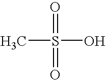
| Organic acids | CH3COOH, CF3COOH, | ||
| HCOOH | |||
| Anhydrides of organic | (CH3CO)2O | ||
| acids | |||
| Dialkylphosphates |
 |
||
| dimethyl hydrogen phosphate | |||
| Alkysphosphates |
 |
||
| methyl dihydrogen phosphate | |||
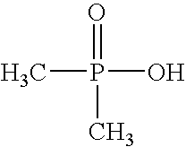
| Phosphonic acids |
 |
||
| methylphosphonic acid | |||
| Phosphinic acids |
 |
||
| dimethylphosphinic acid | |||
| Phosphorus oxides | P2O3, P2O5 | ||
| Alkylamines (primary, | Triethylamine, (CH3CH2)3N | ||
| secondary or tertiary) | |||
| Arylamines |
|
||
| pyridine | |||
| Alky/arylboronic acids |
|
||
| methylboronic acid | |||
| Sulphonic acids |
 |
||
| methanesulfonic acid | |||
| Water | H2O | ||
| Ammonium salts | Tetraethylammonium | ||
| chloride, (CH3CH2)4N+Cl− | |||
| Phosphonitrile | TMSO(PCl2═N)n—P(O)Cl2 | ||
| compounds | |||
| Boron triflates | (CH3CH2)3B(CF3COOH)3 | ||
| Inorganic acids | H2SO4, HCl, HNO3, HF, | ||
| HBr, HI | |||
| Anhydrides of | SO3, N2O5, NO, SO2 | ||
| inorganic acids | |||
Claims (28)


Priority Applications (1)
| Application Number | Priority Date | Filing Date | Title |
|---|---|---|---|
| US11/318,268 US7491653B1 (en) | 2005-12-23 | 2005-12-23 | Metal-free catalysts for pulsed deposition layer process for conformal silica laminates |
Applications Claiming Priority (1)
| Application Number | Priority Date | Filing Date | Title |
|---|---|---|---|
| US11/318,268 US7491653B1 (en) | 2005-12-23 | 2005-12-23 | Metal-free catalysts for pulsed deposition layer process for conformal silica laminates |
Publications (1)
| Publication Number | Publication Date |
|---|---|
| US7491653B1 true US7491653B1 (en) | 2009-02-17 |
Family
ID=40349291
Family Applications (1)
| Application Number | Title | Priority Date | Filing Date |
|---|---|---|---|
| US11/318,268 Expired - Fee Related US7491653B1 (en) | 2005-12-23 | 2005-12-23 | Metal-free catalysts for pulsed deposition layer process for conformal silica laminates |
Country Status (1)
| Country | Link |
|---|---|
| US (1) | US7491653B1 (en) |
Cited By (3)
| Publication number | Priority date | Publication date | Assignee | Title |
|---|---|---|---|---|
| US20080241423A1 (en) * | 2007-03-30 | 2008-10-02 | Blackwell James M | High k dielectric growth on metal triflate or trifluoroacetate terminated iii-v semiconductor surfaces |
| US7625820B1 (en) | 2006-06-21 | 2009-12-01 | Novellus Systems, Inc. | Method of selective coverage of high aspect ratio structures with a conformal film |
| WO2012106600A2 (en) * | 2011-02-04 | 2012-08-09 | Applied Materials, Inc. | In situ vapor phase surface activation of sio2 |
Citations (65)
| Publication number | Priority date | Publication date | Assignee | Title |
|---|---|---|---|---|
| JPH05308071A (en) | 1992-04-30 | 1993-11-19 | Kojundo Chem Lab Co Ltd | Manufacture of silicon oxide film of semiconductor device |
| US5314724A (en) | 1991-01-08 | 1994-05-24 | Fujitsu Limited | Process for forming silicon oxide film |
| US5525550A (en) | 1991-05-21 | 1996-06-11 | Fujitsu Limited | Process for forming thin films by plasma CVD for use in the production of semiconductor devices |
| US5527561A (en) | 1991-05-28 | 1996-06-18 | Electrotech Limited | Method for filing substrate recesses using elevated temperature and pressure |
| US5597395A (en) | 1995-11-28 | 1997-01-28 | Corning Incorporated | Method for low temperature precompaction of glass |
| US5705028A (en) | 1993-04-21 | 1998-01-06 | Yamaha Corporation | Method of manufacturing a semiconductor device with flattened multi-layer wirings |
| US5985770A (en) | 1997-08-21 | 1999-11-16 | Micron Technology, Inc. | Method of depositing silicon oxides |
| US6030881A (en) | 1998-05-05 | 2000-02-29 | Novellus Systems, Inc. | High throughput chemical vapor deposition process capable of filling high aspect ratio structures |
| US6064104A (en) | 1996-01-31 | 2000-05-16 | Advanced Micro Devices, Inc. | Trench isolation structures with oxidized silicon regions and method for making the same |
| US6102993A (en) | 1998-08-03 | 2000-08-15 | Advanced Technology Materials, Inc. | Copper precursor composition and process for manufacture of microelectronic device structures |
| US6133160A (en) | 1998-02-27 | 2000-10-17 | Semiconductor Process Laboratory Co., Ltd. | Method for reforming undercoating surface and method for production of semiconductor device |
| US6184143B1 (en) | 1997-09-08 | 2001-02-06 | Hitachi, Ltd. | Semiconductor integrated circuit device and fabrication process thereof |
| US6300219B1 (en) | 1999-08-30 | 2001-10-09 | Micron Technology, Inc. | Method of forming trench isolation regions |
| US6316063B1 (en) | 1999-12-15 | 2001-11-13 | Intel Corporation | Method for preparing carbon doped oxide insulating layers |
| US6335261B1 (en) | 2000-05-31 | 2002-01-01 | International Business Machines Corporation | Directional CVD process with optimized etchback |
| US6352943B2 (en) | 1998-05-20 | 2002-03-05 | Semiconductor Process Laboratory Co., Ltd. | Method of film formation and method for manufacturing semiconductor device |
| US6352953B1 (en) | 1998-06-30 | 2002-03-05 | Japan Polyolefins Co., Ltd. | Catalyst containing novel transition metal compound for polymerization of olefins |
| WO2002027063A2 (en) | 2000-09-28 | 2002-04-04 | President And Fellows Of Harward College | Vapor deposition of oxides, silicates and phosphates |
| US6479404B1 (en) * | 2000-08-17 | 2002-11-12 | Agere Systems Inc. | Process for fabricating a semiconductor device having a metal oxide or a metal silicate gate dielectric layer |
| US6504233B1 (en) | 1999-06-28 | 2003-01-07 | General Electric Company | Semiconductor processing component |
| US6503330B1 (en) | 1999-12-22 | 2003-01-07 | Genus, Inc. | Apparatus and method to achieve continuous interface and ultrathin film during atomic layer deposition |
| US20030015764A1 (en) | 2001-06-21 | 2003-01-23 | Ivo Raaijmakers | Trench isolation for integrated circuit |
| US6511539B1 (en) | 1999-09-08 | 2003-01-28 | Asm America, Inc. | Apparatus and method for growth of a thin film |
| US6531377B2 (en) | 2001-07-13 | 2003-03-11 | Infineon Technologies Ag | Method for high aspect ratio gap fill using sequential HDP-CVD |
| US6534802B1 (en) | 2001-05-07 | 2003-03-18 | Newport Fab, Llc | Method for reducing base to collector capacitance and related structure |
| US6534395B2 (en) | 2000-03-07 | 2003-03-18 | Asm Microchemistry Oy | Method of forming graded thin films using alternating pulses of vapor phase reactants |
| US6540838B2 (en) | 2000-11-29 | 2003-04-01 | Genus, Inc. | Apparatus and concept for minimizing parasitic chemical vapor deposition during atomic layer deposition |
| US6551399B1 (en) | 2000-01-10 | 2003-04-22 | Genus Inc. | Fully integrated process for MIM capacitors using atomic layer deposition |
| US6551339B2 (en) | 2001-08-23 | 2003-04-22 | Stas Gavronsky | Acupuncture device with improved needle guide tube |
| US6586349B1 (en) | 2002-02-21 | 2003-07-01 | Advanced Micro Devices, Inc. | Integrated process for fabrication of graded composite dielectric material layers for semiconductor devices |
| US20030129828A1 (en) | 1999-10-02 | 2003-07-10 | Uri Cohen | Methods for making multiple seed layers for metallic interconnects |
| US20030134741A1 (en) | 2002-01-15 | 2003-07-17 | Markus Weisbeck | Catalyst |
| US20030157781A1 (en) | 2001-01-20 | 2003-08-21 | Macneil John | Method of filling trenches |
| US6624091B2 (en) | 2001-05-07 | 2003-09-23 | Applied Materials, Inc. | Methods of forming gap fill and layers formed thereby |
| WO2003083167A1 (en) | 2002-03-28 | 2003-10-09 | President And Fellows Of Harvard College | Vapor deposition of silicon dioxide nanolaminates |
| US20040004247A1 (en) | 2002-07-08 | 2004-01-08 | Micron Technology, Inc. | Memory utilizing oxide-nitride nanolaminates |
| US20040025787A1 (en) | 2002-04-19 | 2004-02-12 | Selbrede Steven C. | System for depositing a film onto a substrate using a low pressure gas precursor |
| US20040044127A1 (en) | 2002-08-22 | 2004-03-04 | Konica Corporation | Organic-inorganic hybrid film, its manufacturing method, optical film, and polarizing film |
| US20040043569A1 (en) | 2002-08-28 | 2004-03-04 | Ahn Kie Y. | Atomic layer deposited HfSiON dielectric films |
| US20040079728A1 (en) | 2002-10-23 | 2004-04-29 | Applied Materials, Inc. | Reactive ion etching for semiconductor device feature topography modification |
| US20040102031A1 (en) | 2002-11-21 | 2004-05-27 | Kloster Grant M. | Low-K dielectric structure and method |
| US6780789B1 (en) | 2002-08-29 | 2004-08-24 | Advanced Micro Devices, Inc. | Laser thermal oxidation to form ultra-thin gate oxide |
| US6784101B1 (en) | 2002-05-16 | 2004-08-31 | Advanced Micro Devices Inc | Formation of high-k gate dielectric layers for MOS devices fabricated on strained lattice semiconductor substrates with minimized stress relaxation |
| JP2004256479A (en) | 2003-02-27 | 2004-09-16 | Tosoh Corp | Material for insulating film containing organic silane compound, method for producing the same and semiconductor device |
| US6802944B2 (en) | 2002-10-23 | 2004-10-12 | Applied Materials, Inc. | High density plasma CVD process for gapfill into high aspect ratio features |
| US20040203254A1 (en) | 2003-04-11 | 2004-10-14 | Sharp Laboratories Of America, Inc. | Modulated temperature method of atomic layer deposition (ALD) of high dielectric constant films |
| US20040206267A1 (en) | 2002-12-23 | 2004-10-21 | Sankar Sambasivan | Aluminum phosphate coatings |
| US20040247787A1 (en) | 2002-04-19 | 2004-12-09 | Mackie Neil M. | Effluent pressure control for use in a processing system |
| US20050054213A1 (en) | 2003-09-05 | 2005-03-10 | Derderian Garo J. | Methods of depositing a silicon dioxide comprising layer in the fabrication of integrated circuitry, and methods of forming trench isolation in the fabrication of integrated circuitry |
| US6867152B1 (en) | 2003-09-26 | 2005-03-15 | Novellus Systems, Inc. | Properties of a silica thin film produced by a rapid vapor deposition (RVD) process |
| US6903005B1 (en) | 2000-08-30 | 2005-06-07 | Micron Technology, Inc. | Method for the formation of RuSixOy-containing barrier layers for high-k dielectrics |
| US6908862B2 (en) | 2002-05-03 | 2005-06-21 | Applied Materials, Inc. | HDP-CVD dep/etch/dep process for improved deposition into high aspect ratio features |
| US6949481B1 (en) | 2003-12-09 | 2005-09-27 | Fasl, Llc | Process for fabrication of spacer layer with reduced hydrogen content in semiconductor device |
| US20050239264A1 (en) | 2004-04-21 | 2005-10-27 | Honeywell International Inc. | Materials suitable for shallow trench isolation |
| US20050271813A1 (en) | 2004-05-12 | 2005-12-08 | Shreyas Kher | Apparatuses and methods for atomic layer deposition of hafnium-containing high-k dielectric materials |
| US6984591B1 (en) | 2000-04-20 | 2006-01-10 | International Business Machines Corporation | Precursor source mixtures |
| US20060038293A1 (en) | 2004-08-23 | 2006-02-23 | Rueger Neal R | Inter-metal dielectric fill |
| US20060087000A1 (en) | 2004-10-22 | 2006-04-27 | Matsushita Electric Industrial Co., Ltd. | Semiconductor device and manufacturing method thereof |
| US20060127578A1 (en) | 2004-12-09 | 2006-06-15 | Xinjian Lei | Precursors for silica or metal silicate films |
| US7097878B1 (en) | 2004-06-22 | 2006-08-29 | Novellus Systems, Inc. | Mixed alkoxy precursors and methods of their use for rapid vapor deposition of SiO2 films |
| US7129189B1 (en) | 2004-06-22 | 2006-10-31 | Novellus Systems, Inc. | Aluminum phosphate incorporation in silica thin films produced by rapid surface catalyzed vapor deposition (RVD) |
| US7148155B1 (en) | 2004-10-26 | 2006-12-12 | Novellus Systems, Inc. | Sequential deposition/anneal film densification method |
| US7202185B1 (en) | 2004-06-22 | 2007-04-10 | Novellus Systems, Inc. | Silica thin films produced by rapid surface catalyzed vapor deposition (RVD) using a nucleation layer |
| US7223707B1 (en) | 2004-12-30 | 2007-05-29 | Novellus Systems, Inc. | Dynamic rapid vapor deposition process for conformal silica laminates |
| US7288463B1 (en) * | 2006-04-28 | 2007-10-30 | Novellus Systems, Inc. | Pulsed deposition layer gap fill with expansion material |
-
2005
- 2005-12-23 US US11/318,268 patent/US7491653B1/en not_active Expired - Fee Related
Patent Citations (74)
| Publication number | Priority date | Publication date | Assignee | Title |
|---|---|---|---|---|
| US5314724A (en) | 1991-01-08 | 1994-05-24 | Fujitsu Limited | Process for forming silicon oxide film |
| US5525550A (en) | 1991-05-21 | 1996-06-11 | Fujitsu Limited | Process for forming thin films by plasma CVD for use in the production of semiconductor devices |
| US5527561A (en) | 1991-05-28 | 1996-06-18 | Electrotech Limited | Method for filing substrate recesses using elevated temperature and pressure |
| JPH05308071A (en) | 1992-04-30 | 1993-11-19 | Kojundo Chem Lab Co Ltd | Manufacture of silicon oxide film of semiconductor device |
| US5705028A (en) | 1993-04-21 | 1998-01-06 | Yamaha Corporation | Method of manufacturing a semiconductor device with flattened multi-layer wirings |
| US5597395A (en) | 1995-11-28 | 1997-01-28 | Corning Incorporated | Method for low temperature precompaction of glass |
| US6184108B1 (en) | 1996-01-31 | 2001-02-06 | Advanced Micro Devices, Inc. | Method of making trench isolation structures with oxidized silicon regions |
| US6064104A (en) | 1996-01-31 | 2000-05-16 | Advanced Micro Devices, Inc. | Trench isolation structures with oxidized silicon regions and method for making the same |
| US5985770A (en) | 1997-08-21 | 1999-11-16 | Micron Technology, Inc. | Method of depositing silicon oxides |
| US6372669B2 (en) | 1997-08-21 | 2002-04-16 | Micron Technology, Inc. | Method of depositing silicon oxides |
| US20010049205A1 (en) | 1997-08-21 | 2001-12-06 | Gurtej S. Sandhu | Method of depositing silicon oxides |
| US6184143B1 (en) | 1997-09-08 | 2001-02-06 | Hitachi, Ltd. | Semiconductor integrated circuit device and fabrication process thereof |
| US6133160A (en) | 1998-02-27 | 2000-10-17 | Semiconductor Process Laboratory Co., Ltd. | Method for reforming undercoating surface and method for production of semiconductor device |
| US6030881A (en) | 1998-05-05 | 2000-02-29 | Novellus Systems, Inc. | High throughput chemical vapor deposition process capable of filling high aspect ratio structures |
| US6352943B2 (en) | 1998-05-20 | 2002-03-05 | Semiconductor Process Laboratory Co., Ltd. | Method of film formation and method for manufacturing semiconductor device |
| US6352953B1 (en) | 1998-06-30 | 2002-03-05 | Japan Polyolefins Co., Ltd. | Catalyst containing novel transition metal compound for polymerization of olefins |
| US6102993A (en) | 1998-08-03 | 2000-08-15 | Advanced Technology Materials, Inc. | Copper precursor composition and process for manufacture of microelectronic device structures |
| US6504233B1 (en) | 1999-06-28 | 2003-01-07 | General Electric Company | Semiconductor processing component |
| US20030092241A1 (en) | 1999-08-30 | 2003-05-15 | Doan Trung Tri | Method of forming trench isolation regions |
| US6300219B1 (en) | 1999-08-30 | 2001-10-09 | Micron Technology, Inc. | Method of forming trench isolation regions |
| US6511539B1 (en) | 1999-09-08 | 2003-01-28 | Asm America, Inc. | Apparatus and method for growth of a thin film |
| US20030129828A1 (en) | 1999-10-02 | 2003-07-10 | Uri Cohen | Methods for making multiple seed layers for metallic interconnects |
| US6316063B1 (en) | 1999-12-15 | 2001-11-13 | Intel Corporation | Method for preparing carbon doped oxide insulating layers |
| US6503330B1 (en) | 1999-12-22 | 2003-01-07 | Genus, Inc. | Apparatus and method to achieve continuous interface and ultrathin film during atomic layer deposition |
| US6551399B1 (en) | 2000-01-10 | 2003-04-22 | Genus Inc. | Fully integrated process for MIM capacitors using atomic layer deposition |
| US6534395B2 (en) | 2000-03-07 | 2003-03-18 | Asm Microchemistry Oy | Method of forming graded thin films using alternating pulses of vapor phase reactants |
| US6984591B1 (en) | 2000-04-20 | 2006-01-10 | International Business Machines Corporation | Precursor source mixtures |
| US6335261B1 (en) | 2000-05-31 | 2002-01-01 | International Business Machines Corporation | Directional CVD process with optimized etchback |
| US6479404B1 (en) * | 2000-08-17 | 2002-11-12 | Agere Systems Inc. | Process for fabricating a semiconductor device having a metal oxide or a metal silicate gate dielectric layer |
| US6903005B1 (en) | 2000-08-30 | 2005-06-07 | Micron Technology, Inc. | Method for the formation of RuSixOy-containing barrier layers for high-k dielectrics |
| US20040043149A1 (en) | 2000-09-28 | 2004-03-04 | Gordon Roy G. | Vapor deposition of metal oxides, silicates and phosphates, and silicon dioxide |
| WO2002027063A2 (en) | 2000-09-28 | 2002-04-04 | President And Fellows Of Harward College | Vapor deposition of oxides, silicates and phosphates |
| US6540838B2 (en) | 2000-11-29 | 2003-04-01 | Genus, Inc. | Apparatus and concept for minimizing parasitic chemical vapor deposition during atomic layer deposition |
| US20030157781A1 (en) | 2001-01-20 | 2003-08-21 | Macneil John | Method of filling trenches |
| US6624091B2 (en) | 2001-05-07 | 2003-09-23 | Applied Materials, Inc. | Methods of forming gap fill and layers formed thereby |
| US6534802B1 (en) | 2001-05-07 | 2003-03-18 | Newport Fab, Llc | Method for reducing base to collector capacitance and related structure |
| US6861334B2 (en) | 2001-06-21 | 2005-03-01 | Asm International, N.V. | Method of fabricating trench isolation structures for integrated circuits using atomic layer deposition |
| US20030015764A1 (en) | 2001-06-21 | 2003-01-23 | Ivo Raaijmakers | Trench isolation for integrated circuit |
| US20040222490A1 (en) | 2001-06-21 | 2004-11-11 | Ivo Raaijmakers | Trench isolation structures for integrated circuits |
| US6531377B2 (en) | 2001-07-13 | 2003-03-11 | Infineon Technologies Ag | Method for high aspect ratio gap fill using sequential HDP-CVD |
| US6551339B2 (en) | 2001-08-23 | 2003-04-22 | Stas Gavronsky | Acupuncture device with improved needle guide tube |
| US20030134741A1 (en) | 2002-01-15 | 2003-07-17 | Markus Weisbeck | Catalyst |
| US6586349B1 (en) | 2002-02-21 | 2003-07-01 | Advanced Micro Devices, Inc. | Integrated process for fabrication of graded composite dielectric material layers for semiconductor devices |
| US20050112282A1 (en) | 2002-03-28 | 2005-05-26 | President And Fellows Of Harvard College | Vapor deposition of silicon dioxide nanolaminates |
| WO2003083167A1 (en) | 2002-03-28 | 2003-10-09 | President And Fellows Of Harvard College | Vapor deposition of silicon dioxide nanolaminates |
| US20040025787A1 (en) | 2002-04-19 | 2004-02-12 | Selbrede Steven C. | System for depositing a film onto a substrate using a low pressure gas precursor |
| US20040247787A1 (en) | 2002-04-19 | 2004-12-09 | Mackie Neil M. | Effluent pressure control for use in a processing system |
| US6908862B2 (en) | 2002-05-03 | 2005-06-21 | Applied Materials, Inc. | HDP-CVD dep/etch/dep process for improved deposition into high aspect ratio features |
| US6784101B1 (en) | 2002-05-16 | 2004-08-31 | Advanced Micro Devices Inc | Formation of high-k gate dielectric layers for MOS devices fabricated on strained lattice semiconductor substrates with minimized stress relaxation |
| US20040004247A1 (en) | 2002-07-08 | 2004-01-08 | Micron Technology, Inc. | Memory utilizing oxide-nitride nanolaminates |
| US20040044127A1 (en) | 2002-08-22 | 2004-03-04 | Konica Corporation | Organic-inorganic hybrid film, its manufacturing method, optical film, and polarizing film |
| US20040043569A1 (en) | 2002-08-28 | 2004-03-04 | Ahn Kie Y. | Atomic layer deposited HfSiON dielectric films |
| US6780789B1 (en) | 2002-08-29 | 2004-08-24 | Advanced Micro Devices, Inc. | Laser thermal oxidation to form ultra-thin gate oxide |
| US20040079728A1 (en) | 2002-10-23 | 2004-04-29 | Applied Materials, Inc. | Reactive ion etching for semiconductor device feature topography modification |
| US6802944B2 (en) | 2002-10-23 | 2004-10-12 | Applied Materials, Inc. | High density plasma CVD process for gapfill into high aspect ratio features |
| US20040102031A1 (en) | 2002-11-21 | 2004-05-27 | Kloster Grant M. | Low-K dielectric structure and method |
| US20040206267A1 (en) | 2002-12-23 | 2004-10-21 | Sankar Sambasivan | Aluminum phosphate coatings |
| JP2004256479A (en) | 2003-02-27 | 2004-09-16 | Tosoh Corp | Material for insulating film containing organic silane compound, method for producing the same and semiconductor device |
| US20040203254A1 (en) | 2003-04-11 | 2004-10-14 | Sharp Laboratories Of America, Inc. | Modulated temperature method of atomic layer deposition (ALD) of high dielectric constant films |
| US20050054213A1 (en) | 2003-09-05 | 2005-03-10 | Derderian Garo J. | Methods of depositing a silicon dioxide comprising layer in the fabrication of integrated circuitry, and methods of forming trench isolation in the fabrication of integrated circuitry |
| US6867152B1 (en) | 2003-09-26 | 2005-03-15 | Novellus Systems, Inc. | Properties of a silica thin film produced by a rapid vapor deposition (RVD) process |
| US6949481B1 (en) | 2003-12-09 | 2005-09-27 | Fasl, Llc | Process for fabrication of spacer layer with reduced hydrogen content in semiconductor device |
| US20050239264A1 (en) | 2004-04-21 | 2005-10-27 | Honeywell International Inc. | Materials suitable for shallow trench isolation |
| US20050271813A1 (en) | 2004-05-12 | 2005-12-08 | Shreyas Kher | Apparatuses and methods for atomic layer deposition of hafnium-containing high-k dielectric materials |
| US7097878B1 (en) | 2004-06-22 | 2006-08-29 | Novellus Systems, Inc. | Mixed alkoxy precursors and methods of their use for rapid vapor deposition of SiO2 films |
| US7202185B1 (en) | 2004-06-22 | 2007-04-10 | Novellus Systems, Inc. | Silica thin films produced by rapid surface catalyzed vapor deposition (RVD) using a nucleation layer |
| US7129189B1 (en) | 2004-06-22 | 2006-10-31 | Novellus Systems, Inc. | Aluminum phosphate incorporation in silica thin films produced by rapid surface catalyzed vapor deposition (RVD) |
| US20060038293A1 (en) | 2004-08-23 | 2006-02-23 | Rueger Neal R | Inter-metal dielectric fill |
| US20060087000A1 (en) | 2004-10-22 | 2006-04-27 | Matsushita Electric Industrial Co., Ltd. | Semiconductor device and manufacturing method thereof |
| US7148155B1 (en) | 2004-10-26 | 2006-12-12 | Novellus Systems, Inc. | Sequential deposition/anneal film densification method |
| US7163899B1 (en) * | 2004-10-26 | 2007-01-16 | Novellus Systems, Inc. | Localized energy pulse rapid thermal anneal dielectric film densification method |
| US20060127578A1 (en) | 2004-12-09 | 2006-06-15 | Xinjian Lei | Precursors for silica or metal silicate films |
| US7223707B1 (en) | 2004-12-30 | 2007-05-29 | Novellus Systems, Inc. | Dynamic rapid vapor deposition process for conformal silica laminates |
| US7288463B1 (en) * | 2006-04-28 | 2007-10-30 | Novellus Systems, Inc. | Pulsed deposition layer gap fill with expansion material |
Non-Patent Citations (64)
| Title |
|---|
| "Atomic Layer Deposition of Metal Oxide Thin Films," A thesis presented by Dennis Michael Hausmann, Harvard University, 186 pages, Jul. 2002. |
| "Customer A low k Gapfill Trikon FlowFill vs FHDP", Novellus Systems, Inc., pp. 1-12. |
| Arno et al., "Fourier Transform Infrared Characterization of Downstream Gas-Phase Species Generated by Tetraethylorthosilicate/Ozone Atmospheric Pressure Reactions", Journal of The Electrochemical Society, 146 (1) 276-280 (1999). |
| Beekmann, et al., "Properties of posttreated low kappa flowfill(TM) films and their stability after etch, resist and polymer strip processes", Microelectronic Engineering 55(2001), pp. 73-79. |
| Cho et al., " Hydroxyl Bond Removal and Film Densification Method for Oxide Films Using Microwave Post Treatment", Novellus Systems, Inc., U.S. Appl. No. 11/280,076, filed Nov. 15, 2005, pp. 1-27. |
| Cho et al., "Localized Energy Pulse Rapid Thermal Anneal Dielectric Film Densification Method", Novellus Systems, Inc., U.S. Appl. No. 11/327,668, filed Jan. 5, 2006, pp. 1-28. |
| Gaillard et al., "Effect of plasma and thermal annealing on chemical vapor deposition dielectrics grown using SIH4-H2O2 gas mixtures", J. Vac. Sci. Technol. A 15(5), Sep./Oct. 1997, pp. 2478-2484. |
| Gaillard et al., "Silicon dioxide chemical vapor deposition using silane and hydrogen peroxide", Rapid Communications, J. Vac. Sci. Technol. B 14(4), Jul./Aug. 1996, pp. 2767-2769. |
| Gordon et al., "A Kinetic Model for Step Coverage by Atomic Layer Deposition in Narrow Holes or Trenches", Chemical Vapor Deposition 2003, 9, No. 2, pp. 73-78. |
| Greer et al., "Method and Apparatus to Reduce the Frequency of Chamber Cleans in Rapid Vapor Deposition (RVD) of Silicon Oxide", Novellus Systems, Inc., filed Jul. 12, 2004, U.S. Appl. No. 10/890,376, pp. 1-25. |
| Hausmann et al., "Aluminum Phosphate Incorporation in Silica Thin Films Produced by Rapid Surface Catalyzed Vapor Deposition (RVD)", Novellus Systems, Inc., filed Jun. 22, 2004, U.S. Appl. No. 10/874,808, pp. 1-21. |
| Hausmann et al., "Plasma Treatments to Improve the Properties of Silica Thin Films Produced by a Rapid Vapor Deposition (RVD)", Novellus Systems, Inc., filed Dec. 23, 2000, U.S. Appl. No. 10/746,274, pp. 1-29. |
| Hausmann et al., "Rapid Vapor Deposition of Highly Conformal Silica Nanolaminates," Science, vol. 308, Oct. 2002, 5 Pages. |
| Hausmann et al., "Silica Thin Films Produced by Rapid Surface Catalyzed Vapor Deposition (RVD) Using a Nucleation Layer", Novellus Systems, Inc., filed Jun. 22, 2004, U.S. Appl. No. 10/875,158, pp. 1-25. |
| Hockele et al., "Flowfill-Process as a New Concept for Inter-Metal-Dielectrics", Siemens AG, Semiconductor Group, 1998, pp. 235-238. |
| Ikeda et al., "The Effects of Alkoxy Functional Groups on Atomospheric-Pressure Chemical Vapor Deposition Using Alkoxysilane and Ozone", J. Electrochem. Soc., vol. 142, No. 5, May 1995, pp. 1659-1662. |
| Moore et al., "Reaction of hydrogen peroxide with organosilanes under chemical vapour deposition conditions", J. Chem. Soc., Dalton Trans., 2000, 2673-2677. |
| Papasouliotis et al., "Conformal Nanolaminate Dielectric Deposition and Etch Back Gap Fill Process and Apparatus," Novellus Systems, Inc., U.S. Appl. No. 11/524,502, filed Sep. 19, 2006, pp. 1-38. |
| Papasouliotis et al., "Dynamic Rapid Vapor Deposition Process for Conformal Silica Laminates", Novellus Systems, Inc., filed Dec. 30, 2004, U.S. Appl. No. 11/027,480, pp. 1-29. |
| Papasouliotis et al., "Methods for Forming High Density, Conformal, Silica Nanolaminate Films Via Pulsed Deposition Layer In Structures of Confined Geometry", Novellus Systems, Inc., filed Dec. 30, 2004, U.S. Appl. No. 11/026,284, pp. 1-24. |
| Papasouliotis et al., "Multi-Step Nanolaminate Dielectric Deposition and Etch Back Gap Fill Process", Novellus Systems, Inc., filed Dec. 30, 2004, U.S. Appl. No. 11/026,563, pp. 1-28. |
| Papasouliotis et al., "Pulsed Deposition Layer Gap Fill With Expansion Material," Novellus Systems, Inc., U.S. Appl. No. 11/414,459, filed Apr. 28, 2006, pp. 1-28. |
| Papasouliotis et al., "Reactive Seam Healing Methods for Improving Film Integrity In Structures of Confined Geometry", Novellus Systems, Inc., U.S. Appl. No. 11/334,762, filed Jan. 17, 2006, pp. 1-24. |
| Papasouliotis, George D., "Optimal Operation of Conformal Silica Deposition Reactors", Novellus Systems, Inc., U.S. Appl. No. 11/077,108, filed Mar. 9, 2005, pp. 1-31. |
| Papasouliotis, George D., "Optimal Operation of Conformal Silica Deposition Reactors", Novellus Systems, Inc., U.S. Appl. No. 11/077,198, filed Mar. 9, 2005, pp. 1-32. |
| Papsouliotis et al., "Method for Controlling Properties of Conformal Silica Nanolaminates Formed by Rapid Vapor Deposition", Novellus Systems, Inc., filed Jun. 22, 2004, U.S. Appl. No. 10/874,696, pp. 1-30. |
| Penka et al., "Integration Aspects of Flowfill and Spin-on-Glass Process for Sub-0.35mum Interconnects", pp. 1-3. |
| Ritala et al., "Atomic Layer Deposition", Handbook of Thin Films Materials, vol. 1, 2002, pp. 103-159. |
| Robl et al., "Integration of Flowfill(R) and Forcefill(R) for cost effective via applications" Sep. 1999, pp. 77-83. |
| Roland et al., "Low Temperature Photochemical Vapor Deposition of SiO2 Using 172 nm Xe2* Excimer Lamp Radiation with Three Oxidant Chemistries: O2, H2O/O2, and H2O2", Chem Mater 2001, 13, 2493-2500. |
| Roland et al., "Theoretical Modeling of SiO2 Photochemical Vapor Deposition and Comparison to Experimental Results for Three Oxidant Chemistries: SiH4+O2, H2O/O2, and H2O2", Chem Mater 2001, 13, 2501-2510. |
| Romet et al., "Modeling of Silicon Dioxide Chemical Vapor Deposition from Tetraethoxysilane and Ozone", Journal of The Electrochemical Society, 148 (2) G82-G90 (2001). |
| Rulkens et al., "Chamber and Chamber Surface Materials to Inhibit Deposition and Methods of Making Same", Novellus Systems, Inc., filed Dec. 23, 2004, U.S. Appl. No. 11/027,388, pp. 1-26. |
| Rulkens et al., "Methods for the Use of Alkoxysilanol Precursors for Vapor Deposition of SiO2 Films", Novellus Systems, Inc., filed Dec. 23, 2004, U.S. Appl. No. 11/021,558, pp. 1-24. |
| Rulkens et al., "Mixed Alkoxy Precursors and Methods of Their Use for Rapid Vapor Deposition of SiO2 Films", Novellus Systems, Inc., filed Jun. 22, 2004, U.S. Appl. No. 10/874,814, pp. 1-26. |
| Tarafdar et al., "Sequential Deposition/Anneal Film Densification Method", Novellus Systems, Inc., filed Oct. 26, 2004, U.S. Appl. No. 10/975,028, pp. 1-34. |
| Taylor et al., "Studies on the reaction between silane and hydrogen peroxide vapour; surface formation of planarized silica layers", J. Chem. Soc., Dalton Trans., 1997, pp. 1049-1053. |
| U.S. Office Action mailed Apr. 13, 2007, from U.S. Appl. No. 11/026,284. |
| U.S. Office Action mailed Apr. 25, 2006, from U.S. Appl. No. 11/021,558. |
| U.S. Office Action mailed Dec. 22, 2005, from U.S. Appl. No. 11/026,563. |
| U.S. Office Action mailed Dec. 30, 2005, from U.S. Appl. No. 11/026,284. |
| U.S. Office Action mailed Dec. 5, 2005, from U.S. Appl. No. 10/746,274. |
| U.S. Office Action mailed Dec. 7, 2005, from U.S. Appl. No. 10/874,808. |
| U.S. Office Action mailed Feb. 24, 2006, from U.S. Appl. No. 11/077,108. |
| U.S. Office Action mailed Jan. 16, 2007, from U.S. Appl. No. 10/874,696. |
| U.S. Office Action mailed Jul. 7, 2006, from U.S. Appl. No. 10/875,158. |
| U.S. Office Action mailed Jun. 23, 2005, from U.S. Appl. No. 10/874,808. |
| U.S. Office Action mailed Mar. 21, 2007, from U.S. Appl. No. 11/414,459. |
| U.S. Office Action mailed Mar. 23, 2007, from U.S. Appl. No. 11/021,558. |
| U.S. Office Action mailed Mar. 24, 2006, from U.S. Appl. No. 10/975,028. |
| U.S. Office Action mailed May 15, 2006, from U.S. Appl. No. 11/027,480. |
| U.S. Office Action mailed May 23, 2006, from U.S. Appl. No. 11/077,198. |
| U.S. Office Action mailed May 24, 2006, from U.S. Appl. No. 11/026,284. |
| U.S. Office Action mailed May 31, 2005, from U.S. Appl. No. 10/746,274. |
| U.S. Office Action mailed May 31, 2006, from U.S. Appl. No. 11/026,563. |
| U.S. Office Action mailed May 8, 2006, from U.S. Appl. No. 11/327,668. |
| U.S. Office Action mailed Nov. 10, 2005, from U.S. Appl. No. 11/021,558. |
| U.S. Office Action mailed Oct. 6, 2005, from U.S. Appl. No. 10/975,028. |
| U.S. Office Action mailed Sep. 22, 2005, from U.S. Appl. No. 10/874,814. |
| U.S. Office Action mailed Sep. 27, 2006, from U.S. Appl. No. 11/021,558. |
| U.S. Office Action mailed Sep. 27, 2006, from U.S. Appl. No. 11/026,284. |
| U.S. Office Action mailed Sep. 29, 2006, from U.S. Appl. No. 11/027,480. |
| Xia et al., "High Aspect Ratio Trench Filling Using Two-Step Subatmospheric Chemical Vapor Deposited Borophosphosilicated Glass for <0.18 mum Device Application", Journal of The Electrochemical Society, 146 (5) 1884-1888 (1999). |
| Xia et al., "High Temperature Subatmospheric Chemical Vapor Deposited Undoped Silicated Glass-A Solution for Next Generation Shallow Trench Isolation", Journal of The Electrochemical Society, 146 (3) 1181-1185 (1999). |
Cited By (7)
| Publication number | Priority date | Publication date | Assignee | Title |
|---|---|---|---|---|
| US7625820B1 (en) | 2006-06-21 | 2009-12-01 | Novellus Systems, Inc. | Method of selective coverage of high aspect ratio structures with a conformal film |
| US7863190B1 (en) | 2006-06-21 | 2011-01-04 | Novellus Systems, Inc. | Method of selective coverage of high aspect ratio structures with a conformal film |
| US20080241423A1 (en) * | 2007-03-30 | 2008-10-02 | Blackwell James M | High k dielectric growth on metal triflate or trifluoroacetate terminated iii-v semiconductor surfaces |
| US7763317B2 (en) * | 2007-03-30 | 2010-07-27 | Intel Corporation | High K dielectric growth on metal triflate or trifluoroacetate terminated III-V semiconductor surfaces |
| WO2012106600A2 (en) * | 2011-02-04 | 2012-08-09 | Applied Materials, Inc. | In situ vapor phase surface activation of sio2 |
| WO2012106600A3 (en) * | 2011-02-04 | 2012-11-08 | Applied Materials, Inc. | In situ vapor phase surface activation of sio2 |
| US8778816B2 (en) | 2011-02-04 | 2014-07-15 | Applied Materials, Inc. | In situ vapor phase surface activation of SiO2 |
Similar Documents
| Publication | Publication Date | Title |
|---|---|---|
| US7288463B1 (en) | Pulsed deposition layer gap fill with expansion material | |
| US7109129B1 (en) | Optimal operation of conformal silica deposition reactors | |
| US7482247B1 (en) | Conformal nanolaminate dielectric deposition and etch bag gap fill process | |
| US7625820B1 (en) | Method of selective coverage of high aspect ratio structures with a conformal film | |
| EP1641958B1 (en) | Methods of forming a phosphorus doped silicon dioxide layer | |
| US7163899B1 (en) | Localized energy pulse rapid thermal anneal dielectric film densification method | |
| US6867152B1 (en) | Properties of a silica thin film produced by a rapid vapor deposition (RVD) process | |
| US7135418B1 (en) | Optimal operation of conformal silica deposition reactors | |
| US7790633B1 (en) | Sequential deposition/anneal film densification method | |
| US7297608B1 (en) | Method for controlling properties of conformal silica nanolaminates formed by rapid vapor deposition | |
| EP0440154B1 (en) | Two step process for forming an oxide layer over a stepped surface of a semiconductor wafer | |
| US5354387A (en) | Boron phosphorus silicate glass composite layer on semiconductor wafer | |
| US7202185B1 (en) | Silica thin films produced by rapid surface catalyzed vapor deposition (RVD) using a nucleation layer | |
| US9611544B2 (en) | Plasma activated conformal dielectric film deposition | |
| US6846745B1 (en) | High-density plasma process for filling high aspect ratio structures | |
| US20020090835A1 (en) | Methods and materials for depositing films on semiconductor substrates | |
| CN109477214A (en) | The deposition of flowable silicon-containing film | |
| US7097878B1 (en) | Mixed alkoxy precursors and methods of their use for rapid vapor deposition of SiO2 films | |
| US7129189B1 (en) | Aluminum phosphate incorporation in silica thin films produced by rapid surface catalyzed vapor deposition (RVD) | |
| US9257302B1 (en) | CVD flowable gap fill | |
| JP3515094B2 (en) | Chemical vapor deposition of silicon oxide films using alkyl siloxane oligomers with ozone | |
| EP0421203B1 (en) | An integrated circuit structure with a boron phosphorus silicate glass composite layer on semiconductor wafer and improved method for forming same | |
| US7271112B1 (en) | Methods for forming high density, conformal, silica nanolaminate films via pulsed deposition layer in structures of confined geometry | |
| US7491653B1 (en) | Metal-free catalysts for pulsed deposition layer process for conformal silica laminates | |
| US7294583B1 (en) | Methods for the use of alkoxysilanol precursors for vapor deposition of SiO2 films |
Legal Events
| Date | Code | Title | Description |
|---|---|---|---|
| AS | Assignment |
Owner name: NOVELLUS SYSTEMS, INC., CALIFORNIA Free format text: ASSIGNMENT OF ASSIGNORS INTEREST;ASSIGNORS:PAPASOULIOTIS, GEORGE D.;CHO, SEON-MEE;RULKENS, RON;AND OTHERS;REEL/FRAME:017621/0270;SIGNING DATES FROM 20060124 TO 20060509 |
|
| STCF | Information on status: patent grant |
Free format text: PATENTED CASE |
|
| FPAY | Fee payment |
Year of fee payment: 4 |
|
| FPAY | Fee payment |
Year of fee payment: 8 |
|
| FEPP | Fee payment procedure |
Free format text: MAINTENANCE FEE REMINDER MAILED (ORIGINAL EVENT CODE: REM.); ENTITY STATUS OF PATENT OWNER: LARGE ENTITY |
|
| LAPS | Lapse for failure to pay maintenance fees |
Free format text: PATENT EXPIRED FOR FAILURE TO PAY MAINTENANCE FEES (ORIGINAL EVENT CODE: EXP.); ENTITY STATUS OF PATENT OWNER: LARGE ENTITY |
|
| STCH | Information on status: patent discontinuation |
Free format text: PATENT EXPIRED DUE TO NONPAYMENT OF MAINTENANCE FEES UNDER 37 CFR 1.362 |
|
| FP | Lapsed due to failure to pay maintenance fee |
Effective date: 20210217 |