US7479455B2 - Method for manufacturing semiconductor wafer - Google Patents

Method for manufacturing semiconductor wafer Download PDF

Info

Publication number
US7479455B2
US7479455B2 US11/157,905 US15790505A US7479455B2 US 7479455 B2 US7479455 B2 US 7479455B2 US 15790505 A US15790505 A US 15790505A US 7479455 B2 US7479455 B2 US 7479455B2
Authority
US
United States
Prior art keywords
wafer
supporting plate
adhesive
grinding
back surface
Prior art date
Legal status (The legal status is an assumption and is not a legal conclusion. Google has not performed a legal analysis and makes no representation as to the accuracy of the status listed.)
Expired - Fee Related, expires
Application number
US11/157,905
Other versions
US20060166462A1 (en
Inventor
Ki-Kwon Jeong
Hyeon Hwang
Current Assignee (The listed assignees may be inaccurate. Google has not performed a legal analysis and makes no representation or warranty as to the accuracy of the list.)
Samsung Electronics Co Ltd
Original Assignee
Samsung Electronics Co Ltd
Priority date (The priority date is an assumption and is not a legal conclusion. Google has not performed a legal analysis and makes no representation as to the accuracy of the date listed.)
Filing date
Publication date
Application filed by Samsung Electronics Co Ltd filed Critical Samsung Electronics Co Ltd
Assigned to SAMSUNG ELECTRONICS CO., LTD. reassignment SAMSUNG ELECTRONICS CO., LTD. ASSIGNMENT OF ASSIGNORS INTEREST (SEE DOCUMENT FOR DETAILS). Assignors: HWANG, HYEON, JEONG, KI-KWON
Publication of US20060166462A1 publication Critical patent/US20060166462A1/en
Application granted granted Critical
Publication of US7479455B2 publication Critical patent/US7479455B2/en
Expired - Fee Related legal-status Critical Current
Adjusted expiration legal-status Critical

Links

Images

Classifications

    • HELECTRICITY
    • H01ELECTRIC ELEMENTS
    • H01LSEMICONDUCTOR DEVICES NOT COVERED BY CLASS H10
    • H01L21/00Processes or apparatus adapted for the manufacture or treatment of semiconductor or solid state devices or of parts thereof
    • H01L21/67Apparatus specially adapted for handling semiconductor or electric solid state devices during manufacture or treatment thereof; Apparatus specially adapted for handling wafers during manufacture or treatment of semiconductor or electric solid state devices or components ; Apparatus not specifically provided for elsewhere
    • H01L21/683Apparatus specially adapted for handling semiconductor or electric solid state devices during manufacture or treatment thereof; Apparatus specially adapted for handling wafers during manufacture or treatment of semiconductor or electric solid state devices or components ; Apparatus not specifically provided for elsewhere for supporting or gripping
    • H01L21/6835Apparatus specially adapted for handling semiconductor or electric solid state devices during manufacture or treatment thereof; Apparatus specially adapted for handling wafers during manufacture or treatment of semiconductor or electric solid state devices or components ; Apparatus not specifically provided for elsewhere for supporting or gripping using temporarily an auxiliary support
    • H01L21/6836Wafer tapes, e.g. grinding or dicing support tapes
    • HELECTRICITY
    • H01ELECTRIC ELEMENTS
    • H01LSEMICONDUCTOR DEVICES NOT COVERED BY CLASS H10
    • H01L21/00Processes or apparatus adapted for the manufacture or treatment of semiconductor or solid state devices or of parts thereof
    • H01L21/02Manufacture or treatment of semiconductor devices or of parts thereof
    • H01L21/04Manufacture or treatment of semiconductor devices or of parts thereof the devices having at least one potential-jump barrier or surface barrier, e.g. PN junction, depletion layer or carrier concentration layer
    • H01L21/18Manufacture or treatment of semiconductor devices or of parts thereof the devices having at least one potential-jump barrier or surface barrier, e.g. PN junction, depletion layer or carrier concentration layer the devices having semiconductor bodies comprising elements of Group IV of the Periodic System or AIIIBV compounds with or without impurities, e.g. doping materials
    • H01L21/30Treatment of semiconductor bodies using processes or apparatus not provided for in groups H01L21/20 - H01L21/26
    • H01L21/302Treatment of semiconductor bodies using processes or apparatus not provided for in groups H01L21/20 - H01L21/26 to change their surface-physical characteristics or shape, e.g. etching, polishing, cutting
    • H01L21/304Mechanical treatment, e.g. grinding, polishing, cutting
    • HELECTRICITY
    • H01ELECTRIC ELEMENTS
    • H01LSEMICONDUCTOR DEVICES NOT COVERED BY CLASS H10
    • H01L21/00Processes or apparatus adapted for the manufacture or treatment of semiconductor or solid state devices or of parts thereof
    • H01L21/02Manufacture or treatment of semiconductor devices or of parts thereof
    • H01L21/04Manufacture or treatment of semiconductor devices or of parts thereof the devices having at least one potential-jump barrier or surface barrier, e.g. PN junction, depletion layer or carrier concentration layer
    • H01L21/18Manufacture or treatment of semiconductor devices or of parts thereof the devices having at least one potential-jump barrier or surface barrier, e.g. PN junction, depletion layer or carrier concentration layer the devices having semiconductor bodies comprising elements of Group IV of the Periodic System or AIIIBV compounds with or without impurities, e.g. doping materials
    • H01L21/30Treatment of semiconductor bodies using processes or apparatus not provided for in groups H01L21/20 - H01L21/26
    • H01L21/302Treatment of semiconductor bodies using processes or apparatus not provided for in groups H01L21/20 - H01L21/26 to change their surface-physical characteristics or shape, e.g. etching, polishing, cutting
    • H01L21/306Chemical or electrical treatment, e.g. electrolytic etching
    • H01L21/30625With simultaneous mechanical treatment, e.g. mechanico-chemical polishing
    • HELECTRICITY
    • H01ELECTRIC ELEMENTS
    • H01LSEMICONDUCTOR DEVICES NOT COVERED BY CLASS H10
    • H01L2221/00Processes or apparatus adapted for the manufacture or treatment of semiconductor or solid state devices or of parts thereof covered by H01L21/00
    • H01L2221/67Apparatus for handling semiconductor or electric solid state devices during manufacture or treatment thereof; Apparatus for handling wafers during manufacture or treatment of semiconductor or electric solid state devices or components; Apparatus not specifically provided for elsewhere
    • H01L2221/683Apparatus for handling semiconductor or electric solid state devices during manufacture or treatment thereof; Apparatus for handling wafers during manufacture or treatment of semiconductor or electric solid state devices or components; Apparatus not specifically provided for elsewhere for supporting or gripping
    • H01L2221/68304Apparatus for handling semiconductor or electric solid state devices during manufacture or treatment thereof; Apparatus for handling wafers during manufacture or treatment of semiconductor or electric solid state devices or components; Apparatus not specifically provided for elsewhere for supporting or gripping using temporarily an auxiliary support
    • H01L2221/68327Apparatus for handling semiconductor or electric solid state devices during manufacture or treatment thereof; Apparatus for handling wafers during manufacture or treatment of semiconductor or electric solid state devices or components; Apparatus not specifically provided for elsewhere for supporting or gripping using temporarily an auxiliary support used during dicing or grinding

Abstract

A method may involve mounting a first supporting plate on an active surface of a wafer using an adhesive. A portion of the back surface of the wafer may be backlapped. A second supporting plate may be mounted on the back surface of the wafer using an adhesive. The first supporting plate may be removed from the active surface of the wafer. Conductive bumps may be provided on the active surface. A backlapping process may include a first grinding process, a second grinding process, and a polishing process. The first and the second supporting plates may be fabricated from a solid material. The adhesive may be an ultraviolet cure adhesive or a thermal cure adhesive.

Description

PRIORITY STATEMENT
This U.S. non-provisional application claims benefit of priority under 35 U.S.C. § 119 from Korean Patent Application No. 2005-6795, filed on Jan. 25, 2005, the entire contents of which are incorporated herein by reference.
BACKGROUND
1. Field of the Invention
The present invention relates in general to a semiconductor manufacturing technique, and more particularly, to a method for manufacturing a semiconductor wafer.
2. Description of the Related Art
Semiconductor package structures may include semiconductor packages implementing conductive bumps. Such semiconductor packages may include, for example, flip chip packages and wafer level packages. Semiconductor packages implementing conductive bumps may be advantageous in electrical and thermal characteristics and mounting area, as compared to wire bonding packages.
Conductive bumps may be provided on semiconductor chips at a wafer level. FIG. 1 is a schematic cross-sectional view of a conventional semiconductor wafer 10 having conductive bumps 16.
Referring to FIG. 1, the semiconductor wafer 10 may have an active surface 11 and a back surface 12. A plurality of integrated circuits 13 may be provided on and/or in the semiconductor wafer 10. Scribe lines 14 may be provided between adjacent integrated circuits 13. I/O pads 15 may be provided on the active surface 11 of the semiconductor wafer 10. Conductive bumps 16 may be provided on the I/O pads 15. The conductive bumps 16 may be fabricated from a conductive material, for example a solder and/or gold (Au). The conductive bumps 16 may serve as external connection terminals to be mechanically and electrically connected to external devices.
The semiconductor wafer 10 may be separated into individual semiconductor chips. The separation process may be achieved via a mechanical sawing technique, for example. Before the sawing process, a portion of a back surface of the semiconductor wafer 10 may be removed. Such a process may be referred to as a backgrinding process and/or a backlapping process. The backlapping process may reduce the thickness of a semiconductor wafer 10. For example, a semiconductor wafer having a diameter of 8 inches may have an initial thickness between 730 μm and 750 μm. A semiconductor wafer having a diameter of 12 inches may have an initial thickness between 780 μm and 800 μm. After a backlapping process, the thickness of semiconductor wafers may be 500 μm or less.
Although conventional fabricating techniques are generally thought to be acceptable, they are not without shortcomings. For example, a backlapping process may cause bending and/or warpage of the semiconductor wafer. If a backlapping process is performed on a semiconductor wafer having conductive bumps, the conductive bumps and/or the semiconductor wafer may be damaged, and/or the conductive bumps may be separated from the semiconductor wafer.
The bending and/or warpage of a semiconductor wafer may result from heat generated during a backlapping process. For example, the coefficient of thermal expansion (CTE) of a main material of the integrated circuits may be different from that of a main material of the wafer, for example silicon. Therefore, the active surface of the semiconductor wafer having the integrated circuits may have a different CTE as compared to that of the back surface of the semiconductor wafer. Such a difference in CTE may create critical faults in the semiconductor wafer, especially one that may have a reduced thickness after a backlapping process.
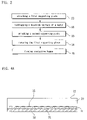
FIG. 2 is a photograph showing warpage of a semiconductor wafer after a backlapping process.
SUMMARY OF THE INVENTION
According to an example, non-limiting embodiment of the invention, a method may involve mounting a first supporting plate on an active surface of a wafer. A portion of a back surface of the wafer may be backlapped. A second supporting plate may be mounted on the back surface of the wafer. Conductive bumps may be provided on the active surface.
According to another example, non-limiting embodiment of the invention, a method may involve mounting a first supporting plate of a solid material on an active surface of a wafer. A portion of a back surface of the wafer may be backlapped. A second supporting plate of a solid material may be mounted on the back surface of the wafer. The first supporting plate may be removed from the active surface of the wafer. Conductive bumps may be provided on the active surface.
According to another example, non-limiting embodiment of the invention, a method may involve mounting a first supporting plate on an active surface of a wafer. A portion of a back surface of the wafer may be removed. A second supporting plate may be mounted on the back surface of the wafer. Conductive bumps may be provided on the active surface.
BRIEF DESCRIPTION OF THE DRAWINGS
Example, non-limiting embodiments of the present invention will be readily understood with reference to the following detailed description thereof provided in conjunction with the accompanying drawings, wherein like reference numerals designate like structural elements.
FIG. 1 is a schematic cross-sectional view of a conventional semiconductor wafer having conductive bumps.
FIG. 2 is a photograph showing warpage of a semiconductor wafer that may occur after a backlapping process.
FIG. 3 is a flow chart of a method that may be implemented to manufacture a semiconductor wafer in accordance with an example, non-limiting embodiment of the present invention.
FIGS. 4A through 4E are schematic cross-sectional views of a method that may be implemented to manufacture a semiconductor wafer in accordance with an example, non-limiting embodiment of the present invention.
These drawings are provided for illustrative purposes only and are not drawn to scale. The spatial relationships and relative sizing of the elements illustrated in the various embodiments may have been reduced, expanded and/or rearranged to improve the clarity of the figure with respect to the corresponding description. The figures, therefore, should not be interpreted as accurately reflecting the relative sizing or positioning of the corresponding structural elements that could be encompassed by an actual device manufactured according to the example, non-limiting embodiments of the invention.
DETAILED DESCRIPTION OF THE EXAMPLE EMBODIMENTS
Example, non-limiting embodiments of the present invention will now be described more fully with reference to the accompanying drawings. This invention may, however, be embodied in many different forms and should not be construed as limited to the example embodiments set forth herein. Rather, the disclosed embodiments are provided so that this disclosure will be thorough and complete, and will fully convey the scope of the invention to those skilled in the art. The principles and features of this invention may be employed in varied and numerous embodiments without departing from the scope of the invention.
Well-known structures and processes are not described or illustrated in detail to avoid obscuring the present invention.
An element is considered as being mounted (or provided) “on” another element when mounted (or provided) either directly on the referenced element or mounted (or provided) on other elements overlaying the referenced element. Throughout this disclosure, the terms “upper,” “lower” “top” and “back” are used for convenience in describing various elements or portions or regions of the elements as shown in the figures. These terms do not, however, require that the structure be maintained in any particular orientation.
FIG. 3 is a flow chart of a method that may be implemented to manufacture a semiconductor wafer in accordance with an example, non-limiting embodiment of the present invention.
In this example embodiment, the method may involve attaching a first supporting plate to an active surface of a wafer (at 21). A portion of a back surface of the wafer may be removed (at 22). A second supporting plate may be attached to the back surface of the wafer (at 23). The first supporting plate may be removed (at 24). Conductive bumps may be provided on the active surface of the wafer (at 25).
FIGS. 4A through 4E are schematic cross-sectional views of a method that may be implemented to manufacture a semiconductor wafer in accordance with an example, non-limiting embodiment of the present invention.
Referring to FIG. 4A, a wafer 10 may have an active surface 11 and a back surface 12. I/O pads 15 may be provided on the active surface 11 of the wafer 10. A first supporting plate 32 may be mounted on the active surface 11 of the wafer 10. By way of example only, the first supporting plate 32 and the wafer 10 may be held together by a first adhesive 31. In alternative embodiments, the first supporting plate 32 and the wafer 10 may be held together by other alternative fasteners including (but not limited to) screws, nails, clips, staples and/or pins, for example.
The first adhesive 31 may be, for example, a sheet type adhesive that may include an ultraviolet cure adhesive and/or a thermal cure adhesive. In alternative embodiments, numerous other adhesives that are well known in this art may be suitably implemented.
The first supporting plate 32 may prevent the wafer 10 from bending and/or warping during subsequent processing. The first supporting plate 32 may be fabricated from a solid material, for example a glass and/or a plastic. In alternative embodiments, the first supporting plate 32 may be fabricated from numerous other materials that are well known in this art. The first supporting plate 32 may have the same shape as the wafer 10. However, the shape of the first supporting plate 32 may be not limited in this regard.
Referring to FIG. 4B, a portion of the wafer may be removed. This removal process may be implemented via a mechanical process, for example, backlapping. For example, the back surface 12 of the wafer 10 may be backlapped using a grinding wheel 33. The grinding wheel 33 may press against the back surface 12 of the wafer 10 while rotating. The grinding wheel 33 may grind the back surface 12 of the wafer 10. The wafer 10 may be mounted on a chuck table (not shown). The chuck table may rotate in the same or reverse direction to that of the grinding wheel 33.
By way of example only, the backlapping process may include a rough grinding process, a fine grinding process and a polishing process. The rough grinding process may grind the backside surface 12 of the wafer 10 using a grinding wheel having a rough surface. The fine grinding process may grind the backside surface 12 of the wafer 10 using a grinding wheel having a fine surface. The polishing process may polish the backside surface 12 of the wafer 10 using a slurry. In alternative embodiment, more or less grinding and/or polishing processes may be suitably implemented.
For example, a wafer 10 having a diameter of 8 inches may have an initial thickness between 730 μm and 750 μm. A wafer 10 having a diameter of 12 inches may have an initial thickness between 780 μm and 800 μm. The initial thickness may be reduced by hundreds of μm via rough grinding, by about 20 μm via fine grinding, and by about 1 μm to 2 μm via polishing. As a result, the final thickness of the wafer 10 may be 500 μm or less, for example 300 μm. The grinding wheel of the rough grinding process may have a grain size between 300 mesh and 350 mesh, for example about 325 mesh. The grinding wheel of the fine grinding process may have a grain size between 1,500 mesh and 2,500 mesh, for example about 2,000 mesh.
Referring to FIG. 4C, a second supporting plate 35 may be mounted on the back surface 12 of the wafer 10. By way of example only, the second supporting plate 35 and the wafer 10 may be held together by a second adhesive 34. In alternative embodiments, the second supporting plate 35 and the wafer 10 may be held together by other alternative fasteners including (but not limited to) screws, nails, clips, staples and/or pins, for example.
The second adhesive 34 may be, for example, a sheet type adhesive that may include an ultraviolet cure adhesive and/or a thermal cure adhesive. In alternative embodiments, numerous other adhesives that are well known in this art may be suitably implemented.
Referring to FIG. 4D, the first supporting plate 32 may be removed from the active surface 11 of the wafer 10. The first supporting plate 32 may be removed via numerous and alternative techniques that are well known in this art.
The second supporting plate 35 may prevent the wafer 10 from bending and/or warping after the first supporting plate 31 has been removed. The second supporting plate 35 may be fabricated from a solid material, for example a glass and/or a plastic. In alternative embodiments, the second supporting plate 35 may be fabricated from numerous other materials that are well known in this art. The second supporting plate 35 may have the same shape as the wafer 10. However, the shape of the second supporting plate 35 may be not limited in this regard.
In an example embodiment, the second supporting plate 35 may be fabricated from a glass, and the second adhesive 34 may be an ultraviolet cure adhesive. In this way, ultraviolet rays may irradiate the adhesive 34 through the second supporting plate 35.
Referring to FIG. 4E, conductive bumps 16 may be provided on the I/O pads 15 of the wafer 10. The conductive bumps 16 may be fabricated from, for example a solder and/or gold (Au). The conductive bumps 16 may also be fabricated from numerous other alternative materials that are well known in this art. The conductive bumps 16 may be fabricated using a plating method, a stencil printing method and/or a ball mounting method.
A separating process and a package assembly process may be performed. The separating process may involve separating (via a sawing process for example) the wafer 10 into individual substrates. Separating process and package assembly process are well known in this art. The second supporting plate 35 may be removed before or after the separating process.
Although example, non-limiting embodiments of the present invention have been described in detail, it will be understood that many variations and/or modifications of the basic inventive concepts, which may appear to those skilled in the art, will still fall within the spirit and scope of the example embodiments of the present invention as defined in the appended claims.

Claims (22)

1. A method comprising:
mounting a first supporting plate on an active surface of a wafer;
backlapping a portion of a back surface of the wafer, the backlapping including:
a first grinding process for grinding the back surface using a first grinding wheel,
a second grinding process for grinding the back surface using a second grinding
wheel having a grinding surface that is less rough than a grinding surface of the first grinding wheel, and
a polishing process for polishing the back surface using a slurry; mounting a second supporting plate on the back surface of the wafer; and
forming conductive bumps on the active surface after the first supporting plate is removed from the active surface.
2. The method of claim 1, wherein the backlapping reduces a thickness of the wafer from an initial thickness of between 730 μm and 800 μm to a reduced thickness of 500 μm or less.
3. The method of claim 1, wherein the first grinding process reduces the thickness of the wafer by hundreds of μm, the second grinding process reduces the thickness of the wafer by about 20 μm, and the polishing process reduces the thickness of the wafer by about 1 μm to 2 μm.
4. The method of claim 1, wherein the conductive bumps are fabricated from one of a solder and gold.
5. The method of claim 1, wherein the conductive bumps are fabricated using a plating method, a stencil printing method, and a ball mounting method.
6. The method of claim 1, wherein the first grinding wheel has a grain size between 300 mesh and 350 mesh, and the second grinding wheel has a grain size between 1,500 mesh and 2,500 mesh.
7. The method of claim 6, wherein the first grinding wheel has a grain size of about 325 mesh, and the second grinding wheel has a grain size of about 2,000 mesh.
8. The method of claim 1, wherein the first supporting plate is mounted on the wafer using an adhesive.
9. The method of claim 8, wherein the adhesive is a sheet type adhesive.
10. The method of claim 8, wherein the adhesive is one of an ultraviolet cure adhesive and a thermal cure adhesive.
11. The method of claim 1, wherein the first supporting plate is fabricated from a solid material.
12. The method of claim 11, wherein the first supporting plate is fabricated from one of a glass and a plastic.
13. The method of claim 1, wherein the second supporting plate is mounted on the wafer using an adhesive.
14. The method of claim 13, wherein the adhesive is a sheet type adhesive.
15. The method of claim 13, wherein the adhesive is one of an ultraviolet cure adhesive and a thermal cure adhesive.
16. The method of claim 1, wherein the second supporting plate is fabricated from a solid material.
17. The method of claim 16, wherein the second supporting plate is fabricated from one of a glass and a plastic.
18. A method comprising:
mounting a first supporting plate of a solid material on an active surface of a wafer;
backlapping a portion of a back surface of the wafer, the backlapping including:
a first grinding process for grinding the back surface using a first grinding wheel having a grain size between 300 mesh and 350 mesh,
a second grinding process for grinding the back surface using a second grinding wheel having a grain size between 1,500 mesh and 2,500 mesh, and
a polishing process for polishing the back surface using a slurry;
mounting a second supporting plate of a solid material on the back surface of the wafer;
removing the first supporting plate from the active surface of the wafer; and
forming conductive bumps on the active surface after the first supporting plate is removed from the active surface.
19. The method of claim 18, wherein the second supporting plate is fabricated from a glass material.
20. The method of claim 18, wherein the second supporting plate is mounted on the wafer using an adhesive.
21. The method of claim 20, wherein the adhesive is a sheet type adhesive.
22. The method of claim 21, wherein the adhesive is one of an ultraviolet cure adhesive and a thermal cure adhesive.
US11/157,905 2005-01-25 2005-06-22 Method for manufacturing semiconductor wafer Expired - Fee Related US7479455B2 (en)

Applications Claiming Priority (2)

Application Number Priority Date Filing Date Title
KR1020050006795A KR20060085848A (en) 2005-01-25 2005-01-25 Method of fabricating semiconductor wafer having bump forming process after back grinding
KR2005-6795 2005-01-25

Publications (2)

Publication Number Publication Date
US20060166462A1 US20060166462A1 (en) 2006-07-27
US7479455B2 true US7479455B2 (en) 2009-01-20

Family

ID=36697396

Family Applications (1)

Application Number Title Priority Date Filing Date
US11/157,905 Expired - Fee Related US7479455B2 (en) 2005-01-25 2005-06-22 Method for manufacturing semiconductor wafer

Country Status (2)

Country Link
US (1) US7479455B2 (en)
KR (1) KR20060085848A (en)

Cited By (2)

* Cited by examiner, † Cited by third party
Publication number Priority date Publication date Assignee Title
US20070215597A1 (en) * 2006-03-20 2007-09-20 Ngk Insulators, Ltd. Heating device and manufacturing method thereof
US20110233706A1 (en) * 2010-03-23 2011-09-29 Samsung Electronics Co., Ltd. Method For Wafer Level Package and Semiconductor Device Fabricated Using The Same

Families Citing this family (1)

* Cited by examiner, † Cited by third party
Publication number Priority date Publication date Assignee Title
KR100945506B1 (en) * 2007-06-26 2010-03-09 주식회사 하이닉스반도체 Semiconductor substrate and method of manufacturing semiconductor package using the semiconductor substrate

Citations (12)

* Cited by examiner, † Cited by third party
Publication number Priority date Publication date Assignee Title
US20030001283A1 (en) * 2001-06-29 2003-01-02 Takashi Kumamoto Multi-purpose planarizing/back-grind/pre-underfill arrangements for bumped wafers and dies
US20030209310A1 (en) * 2002-05-13 2003-11-13 Fuentes Anastacio C. Apparatus, system and method to reduce wafer warpage
US6667191B1 (en) 2002-08-05 2003-12-23 Asat Ltd. Chip scale integrated circuit package
JP2004031825A (en) 2002-06-27 2004-01-29 Umc Japan Semiconductor device and its manufacturing method
US20040087146A1 (en) * 2002-10-31 2004-05-06 Strasbaugh, A California Corporation Method of preparing whole semiconductor wafer for analysis
US20040147120A1 (en) * 2001-05-03 2004-07-29 Michael Rogalli Process for the back-surface grinding of wafers
JP2004228133A (en) 2003-01-20 2004-08-12 Disco Abrasive Syst Ltd Dividing method of semiconductor wafer
JP2004327464A (en) 2003-04-21 2004-11-18 Enzan Seisakusho:Kk Process for forming semiconductor wafer
US20050085008A1 (en) * 2003-10-21 2005-04-21 Derderian James M. Process for strengthening semiconductor substrates following thinning
US20050161774A1 (en) * 2002-03-28 2005-07-28 Yoshihisa Saimoto Pressure sensitive adhesive film for protection of semiconductor wafer surface and method of protecting semiconductor wafer with the pressure sensitive adhesive film
US20060003550A1 (en) * 2004-07-01 2006-01-05 Agency For Science, Technology And Research Method for ultra thinning bumped wafers for flip chip
US20060008650A1 (en) * 2003-11-19 2006-01-12 Mark Wesselmann Protecting thin semiconductor wafers during back-grinding in high-volume production

Patent Citations (12)

* Cited by examiner, † Cited by third party
Publication number Priority date Publication date Assignee Title
US20040147120A1 (en) * 2001-05-03 2004-07-29 Michael Rogalli Process for the back-surface grinding of wafers
US20030001283A1 (en) * 2001-06-29 2003-01-02 Takashi Kumamoto Multi-purpose planarizing/back-grind/pre-underfill arrangements for bumped wafers and dies
US20050161774A1 (en) * 2002-03-28 2005-07-28 Yoshihisa Saimoto Pressure sensitive adhesive film for protection of semiconductor wafer surface and method of protecting semiconductor wafer with the pressure sensitive adhesive film
US20030209310A1 (en) * 2002-05-13 2003-11-13 Fuentes Anastacio C. Apparatus, system and method to reduce wafer warpage
JP2004031825A (en) 2002-06-27 2004-01-29 Umc Japan Semiconductor device and its manufacturing method
US6667191B1 (en) 2002-08-05 2003-12-23 Asat Ltd. Chip scale integrated circuit package
US20040087146A1 (en) * 2002-10-31 2004-05-06 Strasbaugh, A California Corporation Method of preparing whole semiconductor wafer for analysis
JP2004228133A (en) 2003-01-20 2004-08-12 Disco Abrasive Syst Ltd Dividing method of semiconductor wafer
JP2004327464A (en) 2003-04-21 2004-11-18 Enzan Seisakusho:Kk Process for forming semiconductor wafer
US20050085008A1 (en) * 2003-10-21 2005-04-21 Derderian James M. Process for strengthening semiconductor substrates following thinning
US20060008650A1 (en) * 2003-11-19 2006-01-12 Mark Wesselmann Protecting thin semiconductor wafers during back-grinding in high-volume production
US20060003550A1 (en) * 2004-07-01 2006-01-05 Agency For Science, Technology And Research Method for ultra thinning bumped wafers for flip chip

Cited By (3)

* Cited by examiner, † Cited by third party
Publication number Priority date Publication date Assignee Title
US20070215597A1 (en) * 2006-03-20 2007-09-20 Ngk Insulators, Ltd. Heating device and manufacturing method thereof
US20110233706A1 (en) * 2010-03-23 2011-09-29 Samsung Electronics Co., Ltd. Method For Wafer Level Package and Semiconductor Device Fabricated Using The Same
US8558371B2 (en) 2010-03-23 2013-10-15 Samsung Electronics Co., Ltd. Method for wafer level package and semiconductor device fabricated using the same

Also Published As

Publication number Publication date
US20060166462A1 (en) 2006-07-27
KR20060085848A (en) 2006-07-28

Similar Documents

Publication Publication Date Title
US7482695B2 (en) Stack MCP and manufacturing method thereof
TWI284960B (en) Manufacturing method of semiconductor device
KR100517075B1 (en) Method for manufacturing semiconductor device
US6818550B2 (en) Method of cutting a wafer into individual chips
TWI420640B (en) Semiconductor package device, semiconductor package structure, and method for fabricating the same
US20050085008A1 (en) Process for strengthening semiconductor substrates following thinning
US20030045072A1 (en) Methods of thinning microelectronic workpieces
US10141291B2 (en) Semiconductor device and method of manufacturing the same
US20070138605A1 (en) Adhesive sheet, semiconductor device having the same, multi-stacked package having the same, and methods of manufacturing a semiconductor device and a multi-stacked package
US20020173077A1 (en) Thermally enhanced wafer-level chip scale package and method of fabricating the same
US7479455B2 (en) Method for manufacturing semiconductor wafer
WO2017104169A1 (en) Electronic component, method for manufacturing same, and electronic component manufacturing device
US20080029865A1 (en) Electronic Device and Method For Producing the Same
JP3803214B2 (en) Manufacturing method of semiconductor device
US8592286B2 (en) Ultra-thin wafer system and method of manufacture thereof
US7465368B2 (en) Die molding for flip chip molded matrix array package using UV curable tape
US20070114672A1 (en) Semiconductor device and method of manufacturing the same
CN113053798A (en) Ultrathin crystal thinning and cutting process utilizing tempered glass
JP2000340530A (en) Semiconductor device and manufacture thereof
US6894389B2 (en) Semiconductor device and manufacturing method therefor
JP4107896B2 (en) Semiconductor device and manufacturing method thereof
JP2890855B2 (en) Manufacturing method of semiconductor chip
JP2002299547A (en) Laminated semiconductor device and manufacturing method thereor
JP2006140303A (en) Method for manufacturing semiconductor apparatus
JP2006108254A (en) Manufacturing methods of semiconductor chip and semiconductor device

Legal Events

Date Code Title Description
AS Assignment

Owner name: SAMSUNG ELECTRONICS CO., LTD., KOREA, REPUBLIC OF

Free format text: ASSIGNMENT OF ASSIGNORS INTEREST;ASSIGNORS:JEONG, KI-KWON;HWANG, HYEON;REEL/FRAME:016719/0214

Effective date: 20050524

STCF Information on status: patent grant

Free format text: PATENTED CASE

FPAY Fee payment

Year of fee payment: 4

FPAY Fee payment

Year of fee payment: 8

FEPP Fee payment procedure

Free format text: MAINTENANCE FEE REMINDER MAILED (ORIGINAL EVENT CODE: REM.); ENTITY STATUS OF PATENT OWNER: LARGE ENTITY

LAPS Lapse for failure to pay maintenance fees

Free format text: PATENT EXPIRED FOR FAILURE TO PAY MAINTENANCE FEES (ORIGINAL EVENT CODE: EXP.); ENTITY STATUS OF PATENT OWNER: LARGE ENTITY

STCH Information on status: patent discontinuation

Free format text: PATENT EXPIRED DUE TO NONPAYMENT OF MAINTENANCE FEES UNDER 37 CFR 1.362

FP Lapsed due to failure to pay maintenance fee

Effective date: 20210120