US7479395B2 - Method of monitoring a production process using a linear combination of measured variables with selected weights - Google Patents
Method of monitoring a production process using a linear combination of measured variables with selected weights Download PDFInfo
- Publication number
- US7479395B2 US7479395B2 US10/205,080 US20508002A US7479395B2 US 7479395 B2 US7479395 B2 US 7479395B2 US 20508002 A US20508002 A US 20508002A US 7479395 B2 US7479395 B2 US 7479395B2
- Authority
- US
- United States
- Prior art keywords
- linear combination
- determining
- matrix
- intensities
- weights
- Prior art date
- Legal status (The legal status is an assumption and is not a legal conclusion. Google has not performed a legal analysis and makes no representation as to the accuracy of the status listed.)
- Expired - Fee Related, expires
Links
- 238000000034 method Methods 0.000 title claims abstract description 93
- 238000004519 manufacturing process Methods 0.000 title claims abstract description 33
- 238000012544 monitoring process Methods 0.000 title claims abstract description 14
- 239000011159 matrix material Substances 0.000 claims description 49
- 230000008569 process Effects 0.000 claims description 34
- 238000000295 emission spectrum Methods 0.000 claims description 18
- 238000001020 plasma etching Methods 0.000 claims description 13
- 238000000513 principal component analysis Methods 0.000 claims description 11
- 230000003595 spectral effect Effects 0.000 claims description 10
- 238000000354 decomposition reaction Methods 0.000 claims description 6
- 238000009499 grossing Methods 0.000 claims description 5
- 238000000605 extraction Methods 0.000 abstract description 3
- 238000005530 etching Methods 0.000 description 34
- 230000006870 function Effects 0.000 description 31
- 238000006243 chemical reaction Methods 0.000 description 9
- 238000012545 processing Methods 0.000 description 8
- 239000004065 semiconductor Substances 0.000 description 8
- 230000008859 change Effects 0.000 description 7
- 238000001914 filtration Methods 0.000 description 7
- 230000003287 optical effect Effects 0.000 description 7
- 239000000047 product Substances 0.000 description 7
- 239000000758 substrate Substances 0.000 description 7
- 238000005457 optimization Methods 0.000 description 6
- 239000007789 gas Substances 0.000 description 5
- 238000013528 artificial neural network Methods 0.000 description 4
- 230000008901 benefit Effects 0.000 description 4
- 238000001228 spectrum Methods 0.000 description 4
- 235000012431 wafers Nutrition 0.000 description 4
- XUIMIQQOPSSXEZ-UHFFFAOYSA-N Silicon Chemical compound [Si] XUIMIQQOPSSXEZ-UHFFFAOYSA-N 0.000 description 3
- 238000001514 detection method Methods 0.000 description 3
- 238000011156 evaluation Methods 0.000 description 3
- 239000000463 material Substances 0.000 description 3
- 230000005855 radiation Effects 0.000 description 3
- 229910052710 silicon Inorganic materials 0.000 description 3
- 239000010703 silicon Substances 0.000 description 3
- XKRFYHLGVUSROY-UHFFFAOYSA-N Argon Chemical compound [Ar] XKRFYHLGVUSROY-UHFFFAOYSA-N 0.000 description 2
- VYPSYNLAJGMNEJ-UHFFFAOYSA-N Silicium dioxide Chemical compound O=[Si]=O VYPSYNLAJGMNEJ-UHFFFAOYSA-N 0.000 description 2
- 238000004458 analytical method Methods 0.000 description 2
- 238000001636 atomic emission spectroscopy Methods 0.000 description 2
- 238000007796 conventional method Methods 0.000 description 2
- 238000011161 development Methods 0.000 description 2
- 230000018109 developmental process Effects 0.000 description 2
- 230000003993 interaction Effects 0.000 description 2
- 239000000203 mixture Substances 0.000 description 2
- 239000000126 substance Substances 0.000 description 2
- 238000012546 transfer Methods 0.000 description 2
- 239000013598 vector Substances 0.000 description 2
- XPDWGBQVDMORPB-UHFFFAOYSA-N Fluoroform Chemical compound FC(F)F XPDWGBQVDMORPB-UHFFFAOYSA-N 0.000 description 1
- 230000006978 adaptation Effects 0.000 description 1
- 230000032683 aging Effects 0.000 description 1
- 238000013459 approach Methods 0.000 description 1
- 229910052786 argon Inorganic materials 0.000 description 1
- 230000015572 biosynthetic process Effects 0.000 description 1
- 239000007795 chemical reaction product Substances 0.000 description 1
- 238000004140 cleaning Methods 0.000 description 1
- 230000002860 competitive effect Effects 0.000 description 1
- 238000010276 construction Methods 0.000 description 1
- 238000011109 contamination Methods 0.000 description 1
- 238000005137 deposition process Methods 0.000 description 1
- 238000009792 diffusion process Methods 0.000 description 1
- 230000000694 effects Effects 0.000 description 1
- 238000004868 gas analysis Methods 0.000 description 1
- 238000009776 industrial production Methods 0.000 description 1
- 230000015654 memory Effects 0.000 description 1
- 238000012986 modification Methods 0.000 description 1
- 230000004048 modification Effects 0.000 description 1
- 238000010606 normalization Methods 0.000 description 1
- 230000036961 partial effect Effects 0.000 description 1
- 230000010363 phase shift Effects 0.000 description 1
- 230000009467 reduction Effects 0.000 description 1
- 235000012239 silicon dioxide Nutrition 0.000 description 1
- 239000000377 silicon dioxide Substances 0.000 description 1
- TXEYQDLBPFQVAA-UHFFFAOYSA-N tetrafluoromethane Chemical compound FC(F)(F)F TXEYQDLBPFQVAA-UHFFFAOYSA-N 0.000 description 1
- 238000012549 training Methods 0.000 description 1
Images


Classifications
-
- G—PHYSICS
- G01—MEASURING; TESTING
- G01N—INVESTIGATING OR ANALYSING MATERIALS BY DETERMINING THEIR CHEMICAL OR PHYSICAL PROPERTIES
- G01N21/00—Investigating or analysing materials by the use of optical means, i.e. using sub-millimetre waves, infrared, visible or ultraviolet light
- G01N21/17—Systems in which incident light is modified in accordance with the properties of the material investigated
- G01N21/25—Colour; Spectral properties, i.e. comparison of effect of material on the light at two or more different wavelengths or wavelength bands
-
- H—ELECTRICITY
- H01—ELECTRIC ELEMENTS
- H01L—SEMICONDUCTOR DEVICES NOT COVERED BY CLASS H10
- H01L22/00—Testing or measuring during manufacture or treatment; Reliability measurements, i.e. testing of parts without further processing to modify the parts as such; Structural arrangements therefor
- H01L22/20—Sequence of activities consisting of a plurality of measurements, corrections, marking or sorting steps
- H01L22/26—Acting in response to an ongoing measurement without interruption of processing, e.g. endpoint detection, in-situ thickness measurement
-
- H—ELECTRICITY
- H01—ELECTRIC ELEMENTS
- H01L—SEMICONDUCTOR DEVICES NOT COVERED BY CLASS H10
- H01L22/00—Testing or measuring during manufacture or treatment; Reliability measurements, i.e. testing of parts without further processing to modify the parts as such; Structural arrangements therefor
- H01L22/10—Measuring as part of the manufacturing process
- H01L22/12—Measuring as part of the manufacturing process for structural parameters, e.g. thickness, line width, refractive index, temperature, warp, bond strength, defects, optical inspection, electrical measurement of structural dimensions, metallurgic measurement of diffusions
Definitions
- the present invention relates to a method of monitoring a production process.
- the present invention relates in particular to a method of monitoring a production process for processing a semiconductor substrate in semiconductor fabrication.
- Modern industrial production is generally characterized by a high level of automation.
- a high level of automation is imperative in order to be able to be competitive internationally.
- the etching time is a critical parameter in order to achieve a high-quality result. If the etching time is too short, the layer that will be etched is only incompletely removed. In the event of excessively long etching, for example, active regions may begin to be etched or structures may be under-etched. Both conditions must be avoided by using suitable methods for detecting the correct end point.
- U.S. Pat. No. 5,739,051 likewise discloses a method of determining the end point of a plasma etching process.
- the optical emission of the plasma is likewise used to determine the end point.
- Emission lines that are characteristic of the interaction of the etching gas with the exposed substrate are used for the assessment.
- U.S. Pat. No. 5,737,496 proposes using a neural network.
- the neural network is trained by using a large number of determined measured variables, so that it can subsequently be used for detecting the end point.
- neural networks often learn false signals and patterns, so that misinterpretation can occur.
- Faulty training of the neural network arises, for example, as a result of a change in the emission spectra on account of aging phenomena in the sensors or the occurrence of chamber contamination. Therefore, in U.S. Pat. No. 5,864,773, a virtual sensor system, as it is called, is proposed, in which these changes are taken into account before the actual assessment of the measured variables.
- the intention is to provide a virtual sensor that is free of the effects of chamber-specific or process-specific faults.
- At least one linear combination is formed from the large number of measured variables, the weights of the linear combination are selected such that a predefined curve shape is approximated;
- the method has the advantage that, by using a linear combination of the measured variables with suitably selected weights, a (optimal) signal suitable for determining the respective characteristic variable is generated, which considerably simplifies the extraction of the characteristic variable from the measured variables which, in many cases, becomes possible at all for the first time.
- a linear combination should be understood not only as the procedure of linearly combining measured variables, but also the signal obtained in this way.
- the method provides the advantage that in the event of a change in the production process, the necessary adaptation to the extraction of the characteristic variable can be performed merely by adapting the corresponding measuring software, and no manual working steps, such as the replacement of optical filters, are necessary.
- the measured variables used are the intensities of various wavelengths in an emission spectrum.
- emission spectra contain very detailed information about the process on which the radiation emission is based, for example a chemical reaction.
- very large quantities of data accumulate during the recording of such spectra, from which, using conventional methods, the critical information can be extracted only with great difficulty.
- emission spectra can be used with the inventive method for the online monitoring of production or processing processes.
- the intensities of various wavelengths in a spectral range between 200 and 950 nm to be used.
- the emission spectrum from a plasma process is used.
- Plasma etching processes for structuring material layers play an important part in semiconductor fabrication. The dimensions of the structures produced critically depend on the quality of the etching process used.
- the emission spectrum of the plasma contains a large amount of information which is needed in order to monitor the plasma process.
- Highly developed sensor systems such as “optical emission spectroscopy (OES)” or “residual gas analysis (RGA)” can be used to record the spectra. In this case, it is particularly preferable if the end point of the plasma process is determined as the characteristic variable.
- the predefined curve shape used is a step-like function.
- Step-like functions such as a hyperbolic tangent function, can be examined relatively easily with appropriate evaluation algorithms to see whether the step has already been passed through or not, that is to say whether the value of the function has already jumped from a low value to a higher value. Therefore, if the characteristic variable that will be determined is linked to the occurrence of the step, the characteristic variable can be relatively simply determined automatically. In this case, it is preferable in particular if the step-like function has at least one free parameter to match to the characteristic variable to be determined.
- the measured variables at the predefined times are arranged in a matrix, and a principal component analysis is carried out on the basis of this matrix.
- the principal component analysis is a method to express a matrix A by using its principal vectors or principal components.
- a series of methods can be used. For example, singular value decomposition (SVD) of the matrix A can be calculated.
- the eigenvalues and eigenvectors of the correlation matrix (A T A) of the matrix A can also be calculated.
- other methods for the decomposition of a matrix such as “(nonlinear) partial least squares” of a matrix A can also be used.
- the “left-hand” eigenvectors u i form the matrix U mxm
- the “right-hand” eigenvectors v i form the matrix V nxn .
- the singular values ⁇ i are normally arranged in order of magnitude and represent the proportion which the associated dyadic product u i v T i has in the formation of the overall matrix A.
- the dyadic products u i v T i which have only small singular values ⁇ i , generally do not carry information about the monitored process. Accordingly, real measured matrices of measured variables are generally represented sufficiently well by the dyadic products u i v T i with the 3 to 15 largest singular values ⁇ i .
- a function based on the predefined curve shape and the linear combination is minimized or maximized.
- the important principal components of the measured variable matrix are determined by the minimization (or maximization) of the function.
- the minimization (or maximization) of the function it is possible in a straightforward manner to define those principal components which must be taken into account in order to be able to approximate the predefined curve shape with sufficient accuracy.
- the free parameter of the step-like function is determined. In this way, an optimum signal profile for the measured variable to be determined can be defined in a self-consistent way.
- the measured variables have a noise component which is also found again in a linear combination of the measured variables.
- the smoothing of the linear combination is achieved by using a zero-phase filter.
- the measured variables from a number of sample and/or production runs are used to determine the weights of the linear combination.
- the measured variables from a number of sample and/or production runs are arranged in a matrix (block matrix) and a principal component analysis is carried out on the basis of this matrix.
- FIG. 1 shows a schematic representation of an apparatus for carrying out a first embodiment of the inventive method
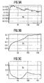
- FIGS. 2A-2C show representations of the first three left-hand eigenvectors of a spectral matrix
- FIGS. 3A-3C show representations of the corresponding first three right-hand eigenvectors of a spectral matrix
- FIG. 4 is a graph of the achievable model quality as a function of the end point t Ep and the number of principal components taken into account;
- FIG. 5 is a graph of the achievable model quality with an optimum C opt i and t Ep as a function of the number of principal components taken into account;
- FIG. 6 shows a representation of an end point pattern u EP ;
- FIG. 7 shows a representation of the linear combination y(t) (generated end point signal) for improving the determination of the end point of a plasma etching operation
- FIG. 8 shows the corresponding conventional signal for determining the end point of a plasma etching operation as known in the prior art
- FIG. 9 shows the course of the linear combination y(t) for some product wafers from three different product cycles
- FIG. 10 shows the course of the corresponding conventional signal as known in the prior art
- FIG. 11 shows the time derivative of the linear combinations y(t) shown in FIG. 9 ;
- FIG. 12 shows the time derivative of the linear combinations y(t) shown in FIG. 9 following filtering
- FIG. 13 shows linear combinations y(t) (continuous lines) with the determined end points (circle) for comparison with the conventional CN signals (dashed) according to the prior art.
- FIG. 1 there is shown a schematic representation of an apparatus for carrying out a first embodiment of the inventive method.
- the significant components of this apparatus are a reaction chamber 1 in which, for example, a plasma etching process (e.g. RIE) can be carried out.
- the etching gas is led via an inlet 2 into the reaction chamber 1 , where it is ionized and converted into a plasma.
- the plasma 9 is generated and maintained by an RF voltage which is applied capacitively and is provided by an RF source 3 .
- the reaction products of the etching are removed from the reaction chamber 1 through an outlet 4 .
- the etching gas used is an etching gas mixture of CF 4 , CHF 3 and argon.
- the homogeneity of the plasma is improved by a magnetic field (not shown) of about 60 gauss.
- the power used to generate and maintain the plasma is about 1200 watts.
- the pressure in the reaction chamber 1 is about 150 mtorr in this case.
- the plasma is used to etch contact holes in a silicon dioxide layer which is arranged on a silicon wafer 5 .
- the silicon wafer 5 is placed on a holder 6 in the reaction chamber 1 .
- the contact holes which are generally used to connect the diffusion regions (active regions) of the transistors, have a very small opening ratio. The requirements on detecting the correct end point of the etching, at which the contact holes reach the silicon substrate, are correspondingly high. If the etching time is too short, the contact holes are not completely opened and the transistors are not connected. If the etching time is too long, the active-regions of the transistors begin to be etched strongly. Both can lead to total failure of the integrated circuit.
- an optical waveguide 10 is arranged at a window of the reaction chamber 1 , and leads to a multichannel spectrometer 7 .
- a multichannel spectrometer from Hamamatsu with the type designation C7460 was used for detecting the optical emission of the plasma.
- This multichannel spectrometer 7 has 1024 channels, which are distributed uniformly over a wavelength range from 200 to 950 nm. With the multichannel spectrometer used, a maximum scanning rate of 50 per second can be achieved. In the present exemplary embodiment, the average emission spectrum of the plasma is measured every 2 seconds.
- the multichannel spectrometer 7 is connected to a data processing system 8 , which continuously records, evaluates and stores the registered spectra.
- the intensities of various wavelengths (1024 different wavelengths in the present case) are recorded over a time period of about 3 min.
- the resulting measured values are arranged in the form of a matrix ⁇ ( ⁇ , t).
- the time profile of a specific wavelength corresponds exactly to one line of the matrix ⁇ ( ⁇ , t).
- the emission spectrum at a specific time is given by exactly one column of the matrix ⁇ ( ⁇ , t).
- the time profiles of the wavelength can also be arranged as the columns of the matrix ⁇ ( ⁇ , t).
- the matrix ⁇ ( ⁇ , t) has 1024 rows and 100 columns.
- a principal component analysis is then carried out on the basis of the matrix ⁇ ( ⁇ , t). To this end, first a matrix ⁇ 0 ( ⁇ , t) is drawn up during trial etching and the weights are determined, which are then used for subsequent etchings.
- the “left-hand” eigenvectors u 0 i form the matrix U 0
- the “right-hand” eigenvectors form the matrix v 0 i .
- FIGS. 3A-3C show representations of the first three left-hand eigenvectors u 0 i from the matrix ⁇ 0 ( ⁇ , t). That is to say the left-hand eigenvectors u 0 i with the three largest singular values ⁇ 0 i .
- FIGS. 3A-3C show representations of the corresponding first three right-hand eigenvectors v 0 i of the matrix ⁇ 0 ( ⁇ , t).
- the columns u 0 i of the matrix U 0 can be interpreted as a basic wavelength pattern, while the columns v 0 i of the matrix V 0 can be interpreted as basic timing signals.
- Y 0 ( t ) ⁇ i ⁇ 0 ( ⁇ , t ) T u 0 i c i .
- the index i indicates the most important left-hand principal components u 0 i from the matrix ⁇ 0 ( ⁇ , T). How many and which of the most important principal components u 0 i can actually be taken into account is determined by the following minimization of a quality function.
- the still unknown coefficients c i are defined in the following minimization of the quality function.
- the function Y 0 (t) is a function of the time t, which can be matched to a predefined curve shape by using the coefficients c i .
- the predefined curve shape is chosen such that the important characteristic variable, in this case the end point of the etching, can be extracted relatively easily from the linear combination.
- the parameter ⁇ is a measure of the desired slope with which the function Y MO (t) jumps from its initial value ( ⁇ 0) to its final value ( ⁇ 1).
- this parameter is predefined externally and is not a variable in the optimization which now follows.
- the parameter t EP specifies the time at which the function Y MO (t) jumps from its initial value ( ⁇ 0) to its final value ( ⁇ 1).
- This parameter t EP is not predefined externally but is defined in the optimization which now follows, so that the end point obtained from the trial run and the parameter t EP agree as well as possible. In this exemplary embodiment, this is achieved by minimizing the quality function Q.
- the sum ⁇ t (or ⁇ t ) here represents a sum of the respective function values at the predefined times.
- FIG. 4 shows a graph of the model quality which can be achieved as a function of the end point t EP and the number of principal components taken into account.
- the optimum selection for the parameter t EP (that point at which the steepest end point signal can be generated) is found by using a one-dimensional numerical optimization. In this case, it is expedient to use a higher-order grid search and then a local gradient-oriented optimization in order to find the optimum t EP opt (n) as a function of the number of principal components taken into account. In this way, disturbances from local minima can be avoided.
- FIG. 5 shows a graph of the achievable model quality Q opt with optimum coefficients c opt i and t EP opt as a function of the number of principal components taken into account.
- the single parameter that still needs to be defined, the number of principal components to be taken into account, can finally be defined.
- FIG. 5 it can be seen that a sufficient model quality is already achieved with four selected principal components.
- FIG. 6 shows a representation of the end point pattern u EP .
- the components U EP j of the end point pattern u EP are the weights looked for, for the linear combination of the intensities of the measured wavelengths from the emission spectrum.
- the end point pattern u EP can be assigned a chemical interpretation.
- CN lines and H lines can be seen clearly.
- FIG. 7 shows a representation of the linear combination y(t) for the improved determination of the end point of a plasma etching operation.
- the linear combination y(t) substantially exhibits a step-like form, which supplies a signal which is substantially sharper and better suited for detecting the correct end point.
- the corresponding conventional end point signal is represented in FIG. 8 .
- the correct end point must be obtained from the position of the small local maximum in the middle of the signal (at about 80 seconds). The determination of the end point by the conventional method is therefore unreliable.
- An evaluation of the linear combination y(t) shown in FIG. 7 then supplies the desired end point of the plasma etching.
- One possible way of evaluating the linear combination y(t) consists in predefining a threshold value (e.g. 0.6). If the linear combination y(t) exceeds the threshold value, the etching process can either be terminated immediately or after the expiration of a certain, fixedly predefined overetch time.
- a threshold value is very simple to implement and supplies satisfactory results for many processes. Unfortunately, this method of determining the characteristic variable generally depends on the absolute magnitudes of the measured value. In the present example, reaching the threshold value depends, for example, on the total intensity of the measured radiation. The total intensity of the measured radiation is a priori unknown, however, so that the correct end point cannot be defined exactly by predefining a threshold value.
- FIG. 9 shows the course of the linear combination y(t) for some production wafers from three different production cycles.
- the resultant end point signals show the successful transfer of the end point pattern to other etching operations.
- the conventional end point signals (CN lines) from the corresponding etching operations are represented again in FIG. 10 .
- a quantitative predefinition of a threshold value (of about 0.6) does not lead exactly to the desired end points, since this threshold value is reached sooner or later, depending on the total intensity of the signal. For this reason, a qualitative signal analysis is subsequently carried out.
- the point of inflection of the linear combination y(t), that is to say, the maximum of the first derivative of the linear combination y(t) with respect to time is therefore used.
- this point of inflection is substantially independent of the total intensity of the measured signal.
- FIG. 11 shows the time derivative of the linear combinations y(t) shown in FIG. 9 .
- the first derivative of the linear combinations y(t) is likewise extremely noisy, so that the maximum of the first derivative cannot be determined in a straightforward way.
- the linear combinations y(t) are first filtered before the first time derivative is formed.
- the filtering By using the filtering, the noise component is suppressed and the actual signal becomes more sharply pronounced.
- FIG. 12 shows the first derivative of the filtered linear combinations y(t). So that the maximum is not shifted during the filtering, the filtering is carried out with a zero-phase filter, as it is known.
- a series of methods or filters can be used.
- the time-discreet variant (sample time T a ) of a Butterworth filter of first order (filter time T F ) was used.
- This filter has the following transfer function C:
- the concrete filtering is carried out by first applying the filter G to the signal y(t) to be filtered. Then, in order to compensate for the phase shift produced during the first filtering, the intermediate signal y* generated in this way is then led via a filter created from the filter G by mirroring the zero and pole positions. Because of the instability of this filter, it is necessary to carry out the implementation in the reverse chronological direction. However, this signifies the same as the renewed application of the original filter G to the signal y* reversed in the chronological direction. The chronological direction of the result of this filtering is then reversed again, in order finally to obtain the desired filtered signal Y F .
- the maximum can now be determined (on line), which corresponds to the points of inflection of the linear combinations y(t) from FIG. 9 .
- the fact that the times found are truly end point specific becomes clear from FIG. 13 .
- the conventional CN signal according to the prior art is shown for comparison. It can be seen clearly that the end point detected using the linear combination y(t) always falls on the rise in the CN signal. This rise is to some extent very flat and varies in its shape, so that it cannot be detected in an automated way.
- contact holes with a very small opening ratio can be produced reproducibly and with high quality in this way.
- the measured variable matrices from the individual processes into a single, large block matrix.
- the weights u EP j obtained in this way now contain the information from a number of etching operations, so that the method can, for example, be used stably over a relatively long time period.
Landscapes
- Physics & Mathematics (AREA)
- Engineering & Computer Science (AREA)
- Life Sciences & Earth Sciences (AREA)
- Chemical & Material Sciences (AREA)
- Power Engineering (AREA)
- Computer Hardware Design (AREA)
- Spectroscopy & Molecular Physics (AREA)
- Health & Medical Sciences (AREA)
- Manufacturing & Machinery (AREA)
- Microelectronics & Electronic Packaging (AREA)
- Analytical Chemistry (AREA)
- Biochemistry (AREA)
- General Health & Medical Sciences (AREA)
- General Physics & Mathematics (AREA)
- Immunology (AREA)
- Pathology (AREA)
- Drying Of Semiconductors (AREA)
Abstract
Description
A=UΣV T=Σiσi u i v T i.
Here, the “left-hand” eigenvectors ui form the matrix Umxm, while the “right-hand” eigenvectors vi form the matrix Vnxn. The singular values σi are normally arranged in order of magnitude and represent the proportion which the associated dyadic product uivT i has in the formation of the overall matrix A. The dyadic products uivT i, which have only small singular values σi, generally do not carry information about the monitored process. Accordingly, real measured matrices of measured variables are generally represented sufficiently well by the dyadic products uivT i with the 3 to 15 largest singular values σi.
Λ0(λ,t)=U 0Σ0 V 0 T=Σiσ0 i u 0 i(v 0 i)T.
Here, the “left-hand” eigenvectors u0 i form the matrix U0, while the “right-hand” eigenvectors form the matrix v0 i.
Y 0(t)=ΣiΛ0(λ,t)T u 0 i c i.
Here, the index i indicates the most important left-hand principal components u0 i from the matrix Λ0(λ, T). How many and which of the most important principal components u0 i can actually be taken into account is determined by the following minimization of a quality function. In addition, the still unknown coefficients ci are defined in the following minimization of the quality function. Once the most important principal components u0 i are defined and the coefficients ci are determined, the linear combination of the measured variables is also defined as a result. On account of the orthogonality of the left-hand principal components u0 i, the function Y0(t) can also be written in the following form:
Y 0(t)=Σi v 0 i(t)σ0 i c i.
The function Y0(t) is a function of the time t, which can be matched to a predefined curve shape by using the coefficients ci. In this case, the predefined curve shape is chosen such that the important characteristic variable, in this case the end point of the etching, can be extracted relatively easily from the linear combination. A typical example of such a curve shape is a hyperbolic tangent function:
Y MO(t)=0.5(tan h[(t−t EP)/δ]+1).
Here, the parameter δ is a measure of the desired slope with which the function YMO(t) jumps from its initial value (≈0) to its final value (≈1). In this example, this parameter is predefined externally and is not a variable in the optimization which now follows. The parameter tEP specifies the time at which the function YMO (t) jumps from its initial value (≈0) to its final value (≈1). This parameter tEP is not predefined externally but is defined in the optimization which now follows, so that the end point obtained from the trial run and the parameter tEP agree as well as possible. In this exemplary embodiment, this is achieved by minimizing the quality function Q. Here:
Q 2=Σt(Y 0(t,c i)−Y MO(t,t EP))2 /N
with the normalization factor,
N=Σ t(Y MO(t,t EP)−Σt′ Y MO(t′,t EP))2.
The sum Σt (or Σt) here represents a sum of the respective function values at the predefined times. By using the minimization of the quality function Q, the most important principal components v0 i are selected, the parameter tEP is optimized, and the coefficients ci are determined. The latter is possible without difficulty because of the orthonormality of the right-hand eigenvectors voi. Thus, the relationship:
C opt i(t EP)=1/σ0 iΣt v 0 i(t)Y MO(t,t EP)
results for the optimum coefficients Copt i, which of course still depend implicitly on the parameter tEP. The choice of the most important principal component u0 i and v0 i is likewise easy to solve, since again, on account of the orthogonality property, the contribution of each principal component to the reduction in the quality function Q can be specified directly. For a specific preselection of principal components, it is merely necessary to select those principal components that have the largest coefficients copt i in terms of magnitude.
u EP=Σi u i c opt i.
y(t)=Λ(λ,t)T u EP.
For the concrete application, a filter time constant TF of 10s was selected, with a sample time Ta of 2s.
Again, the linearly independent spectral basic patterns ui are contained in the matrix U. However, the vectors vi now incorporate the time signal components associated with the spectral basic patterns over a number of etching operations. Accordingly, the desired end point signal YMO(t) must be equipped with n tan h functions arranged one behind another, whose j=1, . . . , n layers tEP j for each etching operation have to be incorporated in the optimization. As a result of the following optimization of the quality function, n different parameters tEP i are then obtained, but only one set of optimum coefficients copt i, from which again an end point pattern uEP can be formed:
u EP=Σi u i c opt i.
However, the weights uEP j obtained in this way now contain the information from a number of etching operations, so that the method can, for example, be used stably over a relatively long time period.
Claims (20)
Applications Claiming Priority (1)
| Application Number | Priority Date | Filing Date | Title |
|---|---|---|---|
| PCT/DE2000/000249 WO2001056072A1 (en) | 2000-01-25 | 2000-01-25 | Method for monitoring a manufacturing process |
Related Parent Applications (1)
| Application Number | Title | Priority Date | Filing Date |
|---|---|---|---|
| PCT/DE2000/000249 Continuation WO2001056072A1 (en) | 2000-01-25 | 2000-01-25 | Method for monitoring a manufacturing process |
Publications (2)
| Publication Number | Publication Date |
|---|---|
| US20030008507A1 US20030008507A1 (en) | 2003-01-09 |
| US7479395B2 true US7479395B2 (en) | 2009-01-20 |
Family
ID=5647408
Family Applications (1)
| Application Number | Title | Priority Date | Filing Date |
|---|---|---|---|
| US10/205,080 Expired - Fee Related US7479395B2 (en) | 2000-01-25 | 2002-07-25 | Method of monitoring a production process using a linear combination of measured variables with selected weights |
Country Status (3)
| Country | Link |
|---|---|
| US (1) | US7479395B2 (en) |
| EP (1) | EP1252652A1 (en) |
| WO (1) | WO2001056072A1 (en) |
Cited By (1)
| Publication number | Priority date | Publication date | Assignee | Title |
|---|---|---|---|---|
| US11153960B1 (en) * | 2018-06-08 | 2021-10-19 | Innoveering, LLC | Plasma-based electro-optical sensing and methods |
Families Citing this family (18)
| Publication number | Priority date | Publication date | Assignee | Title |
|---|---|---|---|---|
| CN1197130C (en) * | 2000-07-04 | 2005-04-13 | 东京毅力科创株式会社 | Operation monitoring method for treatment apparatus |
| DE10208044B8 (en) * | 2002-02-25 | 2009-01-22 | Infineon Technologies Ag | Method and device for monitoring a manufacturing process |
| US8676538B2 (en) * | 2004-11-02 | 2014-03-18 | Advanced Micro Devices, Inc. | Adjusting weighting of a parameter relating to fault detection based on a detected fault |
| FI20041690A0 (en) * | 2004-12-30 | 2004-12-30 | Kone Corp | Lift system |
| FI117091B (en) * | 2005-03-15 | 2006-06-15 | Kone Corp | Transportation control method for destination floor elevator system involves determining transportation device for passenger with respect to traveling time, weighting time and location and selecting device through mobile phone |
| US9075157B2 (en) * | 2012-02-24 | 2015-07-07 | Baker Hughes Incorporated | Bending correction for deep reading azimuthal propagation resistivity |
| US10386828B2 (en) | 2015-12-17 | 2019-08-20 | Lam Research Corporation | Methods and apparatuses for etch profile matching by surface kinetic model optimization |
| US9792393B2 (en) | 2016-02-08 | 2017-10-17 | Lam Research Corporation | Methods and apparatuses for etch profile optimization by reflectance spectra matching and surface kinetic model optimization |
| US10032681B2 (en) | 2016-03-02 | 2018-07-24 | Lam Research Corporation | Etch metric sensitivity for endpoint detection |
| US10197908B2 (en) | 2016-06-21 | 2019-02-05 | Lam Research Corporation | Photoresist design layout pattern proximity correction through fast edge placement error prediction via a physics-based etch profile modeling framework |
| US10254641B2 (en) | 2016-12-01 | 2019-04-09 | Lam Research Corporation | Layout pattern proximity correction through fast edge placement error prediction |
| US10534257B2 (en) | 2017-05-01 | 2020-01-14 | Lam Research Corporation | Layout pattern proximity correction through edge placement error prediction |
| DE102017213147A1 (en) * | 2017-07-31 | 2019-01-31 | Bayerische Motoren Werke Aktiengesellschaft | Method for checking connectors |
| US10572697B2 (en) | 2018-04-06 | 2020-02-25 | Lam Research Corporation | Method of etch model calibration using optical scatterometry |
| US11624981B2 (en) | 2018-04-10 | 2023-04-11 | Lam Research Corporation | Resist and etch modeling |
| US11921433B2 (en) | 2018-04-10 | 2024-03-05 | Lam Research Corporation | Optical metrology in machine learning to characterize features |
| US10977405B2 (en) | 2019-01-29 | 2021-04-13 | Lam Research Corporation | Fill process optimization using feature scale modeling |
| DE202021103238U1 (en) * | 2021-06-16 | 2021-06-22 | TRUMPF Hüttinger GmbH + Co. KG | Signal processing system and power supply device with a signal processing system |
Citations (13)
| Publication number | Priority date | Publication date | Assignee | Title |
|---|---|---|---|---|
| US4609426A (en) * | 1984-05-23 | 1986-09-02 | Hitachi, Ltd. | Method and apparatus for monitoring etching |
| EP0602855A1 (en) | 1992-12-14 | 1994-06-22 | AT&T Corp. | Active neural network control of wafer attributes in a plasma etch process |
| US5658423A (en) * | 1995-11-27 | 1997-08-19 | International Business Machines Corporation | Monitoring and controlling plasma processes via optical emission using principal component analysis |
| US5728253A (en) | 1993-03-04 | 1998-03-17 | Tokyo Electron Limited | Method and devices for detecting the end point of plasma process |
| US5737496A (en) | 1993-11-17 | 1998-04-07 | Lucent Technologies Inc. | Active neural network control of wafer attributes in a plasma etch process |
| US5739051A (en) | 1993-03-04 | 1998-04-14 | Tokyo Electron Limited | Method and device for detecting the end point of plasma process |
| US5864773A (en) | 1995-11-03 | 1999-01-26 | Texas Instruments Incorporated | Virtual sensor based monitoring and fault detection/classification system and method for semiconductor processing equipment |
| US5877032A (en) | 1995-10-12 | 1999-03-02 | Lucent Technologies Inc. | Process for device fabrication in which the plasma etch is controlled by monitoring optical emission |
| WO1999021210A1 (en) | 1997-10-23 | 1999-04-29 | Massachusetts Institute Of Technology | Monitor of plasma processes with multivariate statistical analysis of plasma emission spectra |
| US6381008B1 (en) * | 1998-06-20 | 2002-04-30 | Sd Acquisition Inc. | Method and system for identifying etch end points in semiconductor circuit fabrication |
| US6420194B1 (en) * | 1999-10-12 | 2002-07-16 | Lucent Technologies Inc. | Method for extracting process determinant conditions from a plurality of process signals |
| US6535785B2 (en) * | 1997-09-17 | 2003-03-18 | Tokyo Electron Limited | System and method for monitoring and controlling gas plasma processes |
| US6586262B1 (en) * | 1999-05-18 | 2003-07-01 | Tokyo Electron Limited | Etching end-point detecting method |
-
2000
- 2000-01-25 EP EP00904853A patent/EP1252652A1/en not_active Withdrawn
- 2000-01-25 WO PCT/DE2000/000249 patent/WO2001056072A1/en not_active Application Discontinuation
-
2002
- 2002-07-25 US US10/205,080 patent/US7479395B2/en not_active Expired - Fee Related
Patent Citations (14)
| Publication number | Priority date | Publication date | Assignee | Title |
|---|---|---|---|---|
| US4609426A (en) * | 1984-05-23 | 1986-09-02 | Hitachi, Ltd. | Method and apparatus for monitoring etching |
| EP0602855A1 (en) | 1992-12-14 | 1994-06-22 | AT&T Corp. | Active neural network control of wafer attributes in a plasma etch process |
| US5728253A (en) | 1993-03-04 | 1998-03-17 | Tokyo Electron Limited | Method and devices for detecting the end point of plasma process |
| US5739051A (en) | 1993-03-04 | 1998-04-14 | Tokyo Electron Limited | Method and device for detecting the end point of plasma process |
| US5737496A (en) | 1993-11-17 | 1998-04-07 | Lucent Technologies Inc. | Active neural network control of wafer attributes in a plasma etch process |
| US5877032A (en) | 1995-10-12 | 1999-03-02 | Lucent Technologies Inc. | Process for device fabrication in which the plasma etch is controlled by monitoring optical emission |
| US5864773A (en) | 1995-11-03 | 1999-01-26 | Texas Instruments Incorporated | Virtual sensor based monitoring and fault detection/classification system and method for semiconductor processing equipment |
| US5658423A (en) * | 1995-11-27 | 1997-08-19 | International Business Machines Corporation | Monitoring and controlling plasma processes via optical emission using principal component analysis |
| US6535785B2 (en) * | 1997-09-17 | 2003-03-18 | Tokyo Electron Limited | System and method for monitoring and controlling gas plasma processes |
| WO1999021210A1 (en) | 1997-10-23 | 1999-04-29 | Massachusetts Institute Of Technology | Monitor of plasma processes with multivariate statistical analysis of plasma emission spectra |
| US6153115A (en) * | 1997-10-23 | 2000-11-28 | Massachusetts Institute Of Technology | Monitor of plasma processes with multivariate statistical analysis of plasma emission spectra |
| US6381008B1 (en) * | 1998-06-20 | 2002-04-30 | Sd Acquisition Inc. | Method and system for identifying etch end points in semiconductor circuit fabrication |
| US6586262B1 (en) * | 1999-05-18 | 2003-07-01 | Tokyo Electron Limited | Etching end-point detecting method |
| US6420194B1 (en) * | 1999-10-12 | 2002-07-16 | Lucent Technologies Inc. | Method for extracting process determinant conditions from a plurality of process signals |
Non-Patent Citations (1)
| Title |
|---|
| Whilte et al. "Spatial characterization of wafer state using principal component analysis of optical emission spectra in plasma etch" IEEE transations on semiconductor manufacturing, vol. 10, No. 1, Feb. 1997. * |
Cited By (1)
| Publication number | Priority date | Publication date | Assignee | Title |
|---|---|---|---|---|
| US11153960B1 (en) * | 2018-06-08 | 2021-10-19 | Innoveering, LLC | Plasma-based electro-optical sensing and methods |
Also Published As
| Publication number | Publication date |
|---|---|
| US20030008507A1 (en) | 2003-01-09 |
| EP1252652A1 (en) | 2002-10-30 |
| WO2001056072A1 (en) | 2001-08-02 |
Similar Documents
| Publication | Publication Date | Title |
|---|---|---|
| US7479395B2 (en) | Method of monitoring a production process using a linear combination of measured variables with selected weights | |
| US5653894A (en) | Active neural network determination of endpoint in a plasma etch process | |
| US6368975B1 (en) | Method and apparatus for monitoring a process by employing principal component analysis | |
| EP1210724B1 (en) | Method of determining etch endpoint using principal components analysis of optical emission spectra | |
| US5479340A (en) | Real time control of plasma etch utilizing multivariate statistical analysis | |
| US6564114B1 (en) | Determining endpoint in etching processes using real-time principal components analysis of optical emission spectra | |
| US7169625B2 (en) | Method for automatic determination of semiconductor plasma chamber matching and source of fault by comprehensive plasma monitoring | |
| US6985215B2 (en) | Plasma processing method and plasma processing apparatus | |
| US6745095B1 (en) | Detection of process endpoint through monitoring fluctuation of output data | |
| US8346506B2 (en) | Transforming metrology data from a semiconductor treatment system using multivariate analysis | |
| US7112795B2 (en) | Method of controlling metallic layer etching process and regenerating etchant for metallic layer etching process based on near infrared spectrometer | |
| US20010051437A1 (en) | Process Monitoring Apparatus and Method | |
| White et al. | Low open-area endpoint detection using a PCA-based T/sup 2/statistic and Q statistic on optical emission spectroscopy measurements | |
| DE10230729B4 (en) | A method of detecting the endpoint of an etching process in a semiconductor manufacturing apparatus and detector therefor | |
| KR20230031925A (en) | Control of processing equipment | |
| DE102008029498B4 (en) | Method and system for quantitative in-line material characterization in semiconductor manufacturing based on structural measurements and associated models | |
| Hong et al. | Neural network-based real-time malfunction diagnosis of reactive ion etching using in situ metrology data | |
| KR20220130084A (en) | Plasma treatment apparatus and plasma treatment method | |
| KR101895707B1 (en) | Method of determining an etching end point of plasma process | |
| DE10208044B4 (en) | Method and device for monitoring a manufacturing process | |
| Rangan et al. | Modeling and filtering of optical emission spectroscopy data for plasma etching systems | |
| JP2005033228A (en) | Plasma treatment apparatus and treatment method | |
| JPH11238723A (en) | Method and apparatus for plasma processing | |
| Anderson et al. | In-situ optical emission spectroscopic examination of chrome etch for photomasks | |
| Collard et al. | Examination of various endpoint methods for chrome mask etch |
Legal Events
| Date | Code | Title | Description |
|---|---|---|---|
| AS | Assignment |
Owner name: INFINEON TECHNOLOGIES AG, GERMANY Free format text: ASSIGNMENT OF ASSIGNORS INTEREST;ASSIGNORS:BELL, FERDINAND;KNOBLOCH, DIRK;VOIGTLANDER, KNUT;AND OTHERS;REEL/FRAME:021800/0214;SIGNING DATES FROM 20020608 TO 20020731 |
|
| FEPP | Fee payment procedure |
Free format text: PAYER NUMBER DE-ASSIGNED (ORIGINAL EVENT CODE: RMPN); ENTITY STATUS OF PATENT OWNER: LARGE ENTITY Free format text: PAYOR NUMBER ASSIGNED (ORIGINAL EVENT CODE: ASPN); ENTITY STATUS OF PATENT OWNER: LARGE ENTITY |
|
| STCF | Information on status: patent grant |
Free format text: PATENTED CASE |
|
| CC | Certificate of correction | ||
| FPAY | Fee payment |
Year of fee payment: 4 |
|
| FPAY | Fee payment |
Year of fee payment: 8 |
|
| FEPP | Fee payment procedure |
Free format text: MAINTENANCE FEE REMINDER MAILED (ORIGINAL EVENT CODE: REM.); ENTITY STATUS OF PATENT OWNER: LARGE ENTITY |
|
| LAPS | Lapse for failure to pay maintenance fees |
Free format text: PATENT EXPIRED FOR FAILURE TO PAY MAINTENANCE FEES (ORIGINAL EVENT CODE: EXP.); ENTITY STATUS OF PATENT OWNER: LARGE ENTITY |
|
| STCH | Information on status: patent discontinuation |
Free format text: PATENT EXPIRED DUE TO NONPAYMENT OF MAINTENANCE FEES UNDER 37 CFR 1.362 |
|
| FP | Lapsed due to failure to pay maintenance fee |
Effective date: 20210120 |