US7477885B2 - DC offset cancellation circuits and methods - Google Patents
DC offset cancellation circuits and methods Download PDFInfo
- Publication number
- US7477885B2 US7477885B2 US11/112,174 US11217405A US7477885B2 US 7477885 B2 US7477885 B2 US 7477885B2 US 11217405 A US11217405 A US 11217405A US 7477885 B2 US7477885 B2 US 7477885B2
- Authority
- US
- United States
- Prior art keywords
- offset
- offset cancellation
- coupled
- signal
- circuit
- Prior art date
- Legal status (The legal status is an assumption and is not a legal conclusion. Google has not performed a legal analysis and makes no representation as to the accuracy of the status listed.)
- Active, expires
Links
Images


Classifications
-
- H—ELECTRICITY
- H04—ELECTRIC COMMUNICATION TECHNIQUE
- H04B—TRANSMISSION
- H04B1/00—Details of transmission systems, not covered by a single one of groups H04B3/00 - H04B13/00; Details of transmission systems not characterised by the medium used for transmission
- H04B1/06—Receivers
- H04B1/16—Circuits
- H04B1/30—Circuits for homodyne or synchrodyne receivers
Definitions
- the present invention relates to reducing the effects of DC offset in electronic systems, and in particular, to circuits and methods that may be used to reduce DC offset in an electronic system such as a wireless receiver.
- FIG. 1 illustrates an AC signal, a DC signal and DC offset.
- Waveform 101 is a purely AC waveform because the voltage, V 1 , varies periodically (in this case, sinusoidally) over time and is centered on zero volts.
- Waveform 102 is a purely DC waveform because it maintains the same voltage, V 2 , over time.
- Waveform 103 illustrates an AC waveform with a DC offset. Waveform 103 varies with time, but it is shifted to a voltage V 3 . In this case, waveform 103 is a sinusoid that is offset by a voltage V 3 .
- FIG. 2 illustrates the frequency spectrum of an AC waveform with a DC offset such as waveform 103 .
- waveform 103 may be a sinusoidal signal oscillating at a frequency of f 1 . Therefore, as shown in FIG. 2 , waveform 103 will have a frequency component at f 1 and another component at zero frequency (i.e., DC).
- FIG. 3 illustrates an amplifier circuit that processes both the AC and DC components of a signal.
- Amplifier 300 may receive a varying voltage Vin as an input and generate an output Vout that is an amplified version of the input.
- Vin is a sinusoidal signal with a peak-to-peak amplitude of 400 mV and a DC offset of 1 volt. If amplifier 300 provides a gain of 10, the output Vout will be a sinusoidal signal having a peak-to-peak amplitude of 4 volts and a DC offset of 10 volts.
- FIG. 4 illustrates one of the problems caused by DC offsets in an electronic circuit.
- Non-ideal amplifiers require a power supply Vdd and often include some inherent DC offset.
- amplifier 400 is powered by a 12 volt supply and has an input referred DC offset of 150 mV, which will increase the DC offset of an input signal Vin by 1.5 volts if amplifier 400 has a gain of 10.
- the output should be a sinusoidal signal with a peak-to-peak amplitude of 4 volts and a DC offset of 11.5 volts.
- FIGS. 5A-B illustrate problems caused by DC offset in an analog-to-digital converter.
- amplifier 510 receives an input signal Vin and provides an analog output signal Vout to the input of analog-to-digital converter (“ADC”) 520 .
- ADC 520 converts the analog signal into binary (i.e., digital) values carried by N digital signal lines (i.e., where N is an integer).
- Both amplifier 510 and ADC 520 may, but not necessarily, be powered by the same supply Vdd.
- the range of the ADC is optimized by making Vout as close to the full range of the ADC as possible (the full range of an ADC is typically, but not necessarily, a little less than Vdd).
- FIG. 5B illustrates two signals 501 and 502 .
- Signal 501 is a sinusoidal signal with a DC offset of one-half Vdd (“half-supply”). If the full range of the ADC is from zero volts to Vdd, then signal 501 may be accurately converted because signal 501 varies substantially across the full range, which in this case is an equal amount both above and below half-supply.
- signal 502 when an unwanted DC offset is introduced in a signal, the signal cannot use the full range of the ADC.
- signal 502 is a sinusoidal signal with a DC offset of three-fourths Vdd (i.e., 3Vdd/4). Therefore, signal 502 is limited to a maximum amplitude of one-fourth Vdd. Consequently, half the range of the ADC is lost because of the DC offset.
- DC offsets are caused by a variety of phenomena.
- One source of DC offset is from second order harmonics generated by components of an electronic system.
- Vin e.g., on a gate terminal
- the output signal Vout e.g., on a drain terminal
- Vin is a sinusoidal signal having a frequency ⁇ c
- Vout A Sin( ⁇ c t )+ B Sin 2 ( ⁇ c t )+ C Sin 3 ( ⁇ c t )+ .
- Another source of DC offset in electronic systems is mismatch between electronic components. For example, if resistors are mismatched in a differential system, bias currents through the different resistances may produce a constant voltage difference in the system. More generally, mismatches between electronic components in amplifiers, current sources and other electronic circuits may cause the components operate at different DC operating points. These non-ideal operational conditions of the components often result in a DC offset in the system.
- FIG. 6 illustrates an existing technique for reducing DC offset in a “direct conversion” wireless receiver.
- Wireless receiver 600 includes an antenna 610 for receiving RF signals.
- Antenna 610 is coupled through a switch 601 to a low noise amplifier 611 (“LNA”), mixer 612 , filter 614 , variable gain amplifier 615 (“VGA”) and analog-to-digital converter 616 (“ADC”).
- LNA 611 is used for amplifying high frequency signals from antenna 610 and must have sufficient bandwidth, gain and noise performance to meet system requirements.
- the local oscillator signal (“LO”) is generated by frequency synthesizer 630 .
- Mixer 612 receives a local oscillator signal (“LO”) at the carrier frequency and down converts the input signal.
- Filter 614 is used to extract the signal of interest from the down converted signal, and VGA 615 provides appropriate gain so that the input to ADC 616 is optimizing the ADC's full range.
- the output of the reception channel is coupled to baseband processor 620 over N-bit digital signal lines, for example, for decoding and further processing.
- DC offset in a wireless receiver may have many sources in addition to the sources described above.
- one source of DC offset is from unwanted coupling (sometimes referred to as “leakage” or “feedthrough”) of the local oscillator (“LO”) signal into other parts of the receiver.
- the LO signal is typically a strong signal, and as such may couple into the communication channel and back into antenna 610 .
- the LO signal may also couple to the input of LNA 611 . In both cases the LO signal is boosted by the high gain of the LNA and, consequently, received by mixer 612 on both inputs. This is referred to as “self-mixing.” Self-mixing may also occur when the LO signal couples directly to the input of mixer 612 .
- the DC offset voltage generated at the output of mixer 612 may be very large.
- the LO signal is received on both inputs of mixer 612 , the LO signal is multiplied by itself.
- the DC offset generated by this phenomena can be seen from the following equations wherein the LO signal is modeled as a sinusoidal signal having a frequency ⁇ c :
- Vout ⁇ ⁇ mixer Vin ⁇ ⁇ 1 * Vin ⁇ ⁇ 2
- Vout ⁇ ⁇ mixer ⁇ Sin ⁇ ⁇ ( ⁇ c ⁇ t ) ⁇ ⁇ Sin ⁇ ⁇ ( ⁇ c ⁇ t )
- the mixer output includes a constant component (i.e., 1 ⁇ 2) that has zero frequency.
- This term represents a DC offset at the output of the mixer resulting from self-mixing of the LO signal.
- frequency components of the RF input signal may couple from the input channel to the LO input of the mixer. Such components will also self-mix and result in additional DC offset at the mixer output.
- FIG. 6 further illustrates one existing approach to removing DC offset from a wireless receiver.
- the system is calibrated during a calibration cycle using a feedback loop.
- the ADC measures the DC offset and passes the DC offset value as a digital signal to baseband processor 620 .
- Baseband processor provides a DC offset feedback signal to a digital-to-analog converter 621 (“DAC”).
- DAC digital-to-analog converter
- the output of the DAC is subtracted off the DC offset in the channel at 622 .
- Embodiments of the present invention include circuits and methods for reducing DC offset.
- the present invention includes storing DC offset on internal capacitances.
- parallel stages are used to remove DC offset corresponding to different local oscillator frequencies.
- Other embodiments of the invention include DC offset cancellation circuits with changing cutoff frequencies that may be used to calibrate DC offsets in a very short period of time. In a first state, a the circuits may have a first cutoff frequency, and in a second state the circuits may have a second cutoff frequency lower than the first cutoff frequency.
- the present invention includes a variable gain amplifier circuit including a fixed gain amplifier followed by a DC offset cancellation circuit followed by an attenuator to reduce the effects of DC offset.
- the present invention includes a wireless receiver comprising a mixer having a first input, a second input and an output, wherein the first input is coupled to a first amplifier to receive an amplified RF signal and the second input is coupled to a frequency synthesizer to receive a first signal having one of a plurality of frequencies, and a plurality of parallel DC offset cancellation stages selectively coupled to the mixer output, wherein if the first signal has a first frequency, then a first one of the plurality of parallel DC offset cancellation stages is coupled to the mixer output, and if the first signal has a second frequency, then a second one of the plurality of parallel DC offset cancellation stages is coupled to the mixer output.
- the present invention includes a wireless receiver comprising a first DC offset cancellation circuit, wherein in a first state, the first DC offset cancellation circuit has a first low cutoff frequency, and in a second state, the first DC offset cancellation circuit has a second low cutoff frequency less than the first low cutoff frequency.
- the first DC offset cancellation circuit is coupled between a mixer and a variable gain amplifier.
- the variable gain amplifier includes at least one second DC offset cancellation circuit, wherein in the first state, the second DC offset cancellation circuit has a third low cutoff frequency greater than the first low cutoff frequency of the first DC offset cancellation circuit, and in the second state, the second DC offset cancellation circuit has a fourth low cutoff frequency less than the third low cutoff frequency.
- the present invention includes wireless receiver including a DC offset cancellation circuit, the DC offset cancellation circuit comprising a capacitor having a first terminal coupled to receive an input signal and a second terminal, a first MOS transistor having a first terminal and a second terminal, the first terminal of the MOS transistor being coupled to the second terminal of the capacitor, and a resistance coupled between the second terminal of the first MOS transistor and a reference voltage, wherein, in a first state, the resistance has a first value so that the circuit has a first low cutoff frequency, and in a second state, the resistance has a second value so that the circuit has a second low cutoff frequency less than the first low cutoff frequency.
- FIG. 1 illustrates an AC signal, a DC signal and DC offset.
- FIG. 2 illustrates the frequency spectrum of an AC waveform with a DC offset.
- FIG. 3 illustrates an amplifier circuit that processes both the AC and DC components of a signal.
- FIG. 4 illustrates one of the problems caused by DC offsets in an electronic circuit.
- FIGS. 5A-B illustrate problems caused by DC offset in an analog-to-digital converter.
- FIG. 6 illustrates an existing technique for reducing DC offset in a direct conversion wireless receiver.
- FIG. 7 illustrates a wireless receiver including DC offset cancellation according to one embodiment of the present invention.
- FIGS. 8A-B illustrate another DC offset phenomena addressed by embodiments of the present invention.
- FIG. 9 illustrates a DC offset cancellation circuit according to one embodiment of the present invention.
- FIGS. 10A-B are example implementations of a DC offset cancellation circuit according to one embodiment of the present invention.
- FIG. 11 illustrates another constraint on DC offset cancellation circuits solved by embodiments of the present invention.
- FIGS. 12A-B illustrate a DC offset cancellation circuit according to another embodiment of the present invention.
- FIG. 13 is an example of a differential implementation of a three stage DC offset cancellation circuit according to one embodiment of the present invention.
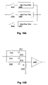
- FIG. 14A illustrates a DC offset cancellation circuit according to another embodiment of the present invention.
- FIGS. 14B-D illustrate a DC offset cancellation circuit according to another embodiment of the present invention.
- FIG. 15 illustrates another embodiment of the present invention.
- FIG. 16 is an example implementation of DC offset cancellation stages with variable attenuation according to another embodiment of the present invention.
- FIG. 17 illustrates part of a variable gain amplifier circuit according to one embodiment of the present invention.
- FIG. 18A illustrates part of a VGA with a DC offset cancellation circuit according to one embodiment of the present invention.
- FIG. 18B illustrates part of a VGA with a DC offset cancellation circuit according to another embodiment of the present invention.
- FIG. 19 illustrates wireless receiver with DC offset cancellation according to another embodiment of the present invention.
- Described herein are techniques for reducing DC offset in electronic systems.
- numerous examples and specific details are set forth in order to provide a thorough understanding of the present invention.
- many of the techniques herein are very complex and are advantageously described using specific examples, such as wireless receivers and ultra-wideband (“UWB”) wireless receivers, to illustrate certain advantages of various embodiments. Therefore, many of the techniques are described in a wireless receiver application.
- UWB ultra-wideband
- embodiments of the present invention may be used in other applications.
- the inventions, as defmed by the claims may include some or all of the features in these examples alone or in combination with other features described below.
- FIG. 7 illustrates a wireless receiver including DC offset cancellation according to one embodiment of the present invention.
- Wireless receiver 700 includes an antenna 710 for receiving a RF signal.
- An RF signal received on antenna 710 is coupled through switch 701 to a low noise amplifier 711 (“LNA”).
- LNA 711 is used for amplifying high frequency signals from antenna 710 and must have sufficient bandwidth, gain and noise performance to meet system requirements.
- the gain of LNA 711 may be adjustable, for example, between 10 dBv and 20 dBv.
- the output of LNA 711 is coupled to one input of mixer 712 .
- the reception channel may include two mixers and parallel paths for both in phase and quadrature paths (only one path is shown here).
- a local oscillator signal (“LO”) is generated by frequency synthesizer 730 .
- LO local oscillator signal
- Mixer 712 receives a local oscillator signal (“LO”) at the carrier frequency and down converts the input signal.
- LO local oscillator signal
- the system is a direct conversion system.
- the input signal is down converted to baseband, and no intermediate frequencies are used.
- the present invention is not limited to direct conversion systems.
- the output of mixer 712 is coupled to filter 714 .
- Filter 714 is used to extract the signal of interest from the down converted signal.
- the present invention includes a DC offset cancellation circuit 715 between filter 714 and a VGA 715 .
- the DC offset cancellation circuit reduces the DC offset from upstream circuits (e.g., mixer 712 and LNA 711 ).
- VGA 715 receives the down converted signal with reduced DC offset and provides appropriate gain so that the input to ADC 716 is at the ADC's full range.
- VGA 715 may be a programmable gain amplifier (“PGA”) that receives digital gain control signals from another part of the system to change the gain in discrete steps.
- PGA programmable gain amplifier
- embodiments of the present invention may include additional DC offset cancellation circuits in VGA 715 for further reducing DC offset in the system.
- the output of the reception channel is coupled to baseband processor 720 over N-bit digital signal lines, for example, for decoding and further processing.
- FIGS. 8A-B illustrate another DC offset phenomena addressed by embodiments of the present invention.
- FIG. 8A illustrates frequency hopping. Some wireless systems may use multiple carrier frequencies that each carry information of interest.
- FIG. 8A illustrates three carrier frequencies f 1 , f 2 , and f 3 used to carry information in three communication channels 801 , 802 , and 803 .
- the channel used to transfer information may change between the three channels 801 , 802 , and 803 during a single communication event (e.g., communication of a data packet).
- the system may receive information on a first carrier frequency, f 1 , and the synthesizer must generate an LO signal at f 1 to down convert the incoming signal.
- the system may change the channel, and the synthesizer must change the frequency of the LO signal to extract the information received on the new channel (e.g., f 2 on channel 802 ).
- These frequency changes are sometimes referred to as “channel hopping,” and such changes between frequencies may occur in a variety of different patterns (e.g., f 1 -f 2 -f 3 -f 1 -f 2 -f 3 or f 1 -f 3 -f 2 -f 1 -f 3 -f 2 ).
- FIG. 8B illustrates different DC offsets generated at different frequencies f 1 , f 2 , and f 3 .
- the output of mixer 712 will have a DC offset of “DC 1 .”
- the output of mixer 712 will have a DC offset of “DC 2 .”
- the output of mixer 712 will have a DC offset of “DC 3 .”
- DC offset cancellation circuit 900 includes first, second, and third DC offset cancellation stages 901 - 903 in parallel and control signals (“Select”) for controlling which stage is active.
- each DC cancellation stage may include an internal capacitance (e.g., a capacitor) for storing different DC offsets corresponding to different LO frequencies.
- a first carrier frequency e.g., f 1 for channel 801
- the system activates DC offset cancellation stage 901 for canceling DC offset corresponding to a first LO frequency.
- each stage may be activated by selectively coupling each stage to the mixer output, for example, by closing internal switches in each circuit.
- FIGS. 10A-B are example implementations of a DC offset cancellation circuit according to one embodiment of the present invention.
- each DC cancellation stage includes a high pass filter.
- FIG. 10A three high pass filters are arranged in parallel and selectively coupled to the mixer output.
- switch 1001 When the system is receiving a signal on a first channel, switch 1001 may be closed so that the input signal passes through high pass filter 1005 .
- switch 1002 When the system is receiving a signal on a second channel, switch 1002 may be closed so that the input signal passes through high pass filter 1006 .
- switch 1003 When the system is receiving a signal on a third channel, switch 1003 may be closed so that the input signal passes through high pass filter 1007 .
- FIG. 10B is an example of one high pass filter configuration that may be used.
- the DC offset cancellation circuit in this example includes three switches 1001 - 1003 in series with three capacitors 1011 - 1013 . Each capacitor is coupled to ground through a resistance 1015 (“R”). It is understood that ground is a reference voltage and other reference voltages may be used.
- R resistance
- DC 1 the DC offset generated at the mixer output corresponding to a first channel (i.e., a first LO signal frequency) may be stored on capacitor 1011 (“C 1 ”).
- DC 2 a new DC offset
- the new DC offset is stored on capacitor 1012 (“C 2 ”).
- a third DC offset (“DC 3 ”) is generated at the mixer output
- switch 1002 is opened and switch 1003 is closed.
- the third DC offset is stored on capacitor 1013 (“C 3 ”).
- the down converted signals received from the mixer may be passed for further amplification in amplifier 1020 , which may be the first stage of a VGA, for example.
- FIG. 11 is an example of another constraint on DC offset cancellation circuits solved by embodiments of the present invention.
- DC offset is calibrated before such an event (i.e., while the system is idle), incoming data may be lost if the data is received while the system in the middle of a calibration cycle.
- calibrated DC levels may need to be periodically refreshed if the system remains idle for an extended period of time.
- FIG. 11 shows a preamble 1101 and payload 1102 of an incoming packet in a packet based protocol received by a wireless system at the beginning of a communication.
- the preamble may be used for synchronization, determining a frequency hopping pattern, and gain adjustment, for example.
- An example preamble may include 21 symbols 1110 that are each about 310 ns in duration, such as is found in an 802.15 protocol.
- Each symbol may include a plurality of subcarriers spread across a frequency range, such as orthogonal frequency division multiplexing (“OFDM”) signals.
- OFDM orthogonal frequency division multiplexing
- each symbol may be received on a different frequency channel, and the first symbol may indicate to the receiving system when and how the frequency channels will change (i.e., the first symbol may contain the frequency hopping pattern indicating when the incoming signal will change channels and what the next channel will be).
- the system may go through a calibration cycle and change the gain of the receiver.
- DC offset should not cause too much signal loss or distortion (e.g., if the receiver becomes saturated) or else the gain adjust and other preamble functions will not be completed accurately. Accordingly, DC offset must be cancelled quickly during reception of the preamble. For instance, some applications may only allocate 10 or 20 percent of each symbol (e.g., about 40-66 ns) for DC offset circuits to complete the DC cancellation process. Moreover, some embodiments may require that the receiver process signals while the DC offset circuits are in the process of calibrating the unwanted DC offsets.
- FIGS. 12A-B illustrate a DC offset cancellation circuit according to another embodiment of the present invention.
- FIG. 12A shows a DC offset correction circuit 1200 that may be used in one channel of the multi-channel circuit of FIG. 9 , and includes additional circuitry for DC offset cancellation, for example, when the system is receiving symbols.
- the DC offset cancellation circuit operates in two states. In the first state (e.g., a calibration state), the circuit is configured to have a first low cutoff frequency high enough to allow the circuit to accurately capture the DC offset in a short time period. In the second state, the circuit is configured to have a second low cutoff frequency low enough to pass all frequencies of interest.
- the system may close switches 1201 and 1202 , thereby placing the circuit in the signal path and further configuriing R 1 and R 2 in parallel. Since the resistance of a parallel combination of resistors R 1 and R 2 is less than the resistance of R 1 alone, the low cutoff frequency increases when switch 1202 is closed (i.e., R decreases so f c , increases). If DC offset from the mixer causes an increase in the voltage on capacitor 1212 (“C 2 ”), such increase will cause a corresponding increase on the filter output. However, the output of the filter will discharge back to zero volts through resistors R 1 and R 2 . It is desirable to accurately store the DC offset on capacitor C 2 .
- the system may reconfigure the circuit to have a second cutoff frequency low enough to pass all frequencies of interest. For example, in a second state, the system may open switch 1202 , thereby increasing R and reducing the low cutoff frequency. As shown in FIG. 12B , some information carrying signals (e.g., s 1 and s 2 ) may be below the low cutoff frequency of the circuit during DC offset calibration. Some applications may tolerate the loss of some information carrying signals during the calibration cycle, but require that such signals not be lost during normal operation. Accordingly, after a predetermined time period when the DC offset is stored on capacitor C 2 , the system may reconfigure the circuit to have a second cutoff frequency low enough to pass all frequencies of interest. For example, in a second state, the system may open switch 1202 , thereby increasing R and reducing the low cutoff frequency. As shown in FIG.
- the low cutoff frequency moves from ⁇ c1 to ⁇ c2 .
- all the information carrying signals may pass through the circuit (e.g., s 1 and s 2 will be above the cutoff frequency in the second state rather than below the cutoff frequency as in the first state).
- a variety of low cutoff frequencies may be used to reduce the RC time constant of the circuit or pass signals of interest, and a variety of time periods may be used to accurately capture the DC offset. Such implementation details will be matters of design choice governed by the design requirements of the application.
- An example application of this technique is in a wireless receiver that receives 21 symbols in a preamble at the beginning of each communication transaction.
- each symbol is 310 ns, and different symbols may be received on different carrier frequencies (i.e., different LO frequencies are used to down convert the incoming RF signal carrying different symbols).
- the first symbol may be received on carrier frequency f 1
- the second symbol may be received on carrier frequency f 2
- the third symbol may be received on carrier frequency f 3 .
- each symbol may include a plurality of subcarriers (e.g., s 1 , s 2 , . . . , sN) spaced at certain frequency intervals (e.g., 4.125 MHz).
- subcarriers e.g., s 1 , s 2 , . . . , sN
- DC offset may be captured on capacitor C 2 for a first portion of the symbol (e.g., about the first 20% of the symbol, which is 20% of 310 ns, or about 66 ns). Therefore, when the first symbol is received, the DC offset correction circuit will initially be configured in a first state wherein the time to accurately store the DC offset on the capacitor is less than a predetermined portion of the total symbol time.
- switch 1202 may be closed so the resistance to ground is reduced and the time constant of the circuit reduced (i.e., the low cutoff frequency is increased).
- the RC time constant will also set the cutoff frequency of the circuit.
- R 1 , R 2 and C 2 should be selected so that the RC time constant is low enough to allow sufficiently fast and accurate storage of the DC offset on capacitor C 2 , but high enough to result in a cutoff frequency that allows as many of the subcarriers to pass as possible.
- the system may receive the information in the first symbol above the cutoff frequency. It is to be understood that the cutoff frequency and time constant are only examples and that a variety of other implementations may be used depending on the requirements of the particular system.
- the system may reconfigure circuit 1200 into a second state by opening switch 1202 , and thereby removing R 2 from the circuit.
- the DC offset is removed from the signal path because such offset is stored on capacitor C 2 .
- the cutoff frequency is reduced because R 2 is no longer in parallel with R 1 .
- the cutoff frequency in the second state may be 1 Mhz.
- the first symbol, or even the first two symbols may be received on a first carrier frequency f 1 , but the system may change to other carrier frequencies f 2 or f 3 to carry other symbols. As also described above, this frequency hopping may cause the DC offset to change. Accordingly, the DC offset cancellation process using multiple low cutoff frequencies may be applied to each new carrier frequency received by the system, so that the new DC offset generated from down conversion of a new carrier frequency can be eliminated. For example, if the hopping pattern is [f 1 , f 2 , f 3 , f 1 , f 2 , f 3 . . .
- the system will reconfigure itself to receive the second symbol at frequency f 2 by deactivating a first DC offset correction circuit and activating a second DC offset correction circuit.
- the system will reconfigure itself to receive the third symbol at frequency f 3 by deactivating the second DC offset correction circuit and activating a third DC offset correction circuit.
- the system may reconfigure between the first cutoff frequency and the second lower cutoff frequency after all DC offset cancellation circuits have stored DC calibration voltages.
- all of the DC offset cancellation circuits may be configured in the first state until each channel in a frequency hopping pattern has been received and DC offsets corresponding to each frequency have been calibrated.
- the system may then reconfigure into the second state.
- a specific example may be if the frequency hopping pattern were [f 1 , f 2 , f 3 , f 1 , f 2 , f 3 , f 1 , . . . ].
- the system would be in the first state while the system is receiving the first three frequencies (i.e., after the first occurrence of f 1 , f 2 , and f 3 ), and the system may reconfigure after the first pattern cycle (here, after the third symbol). If the pattern were [f 1 , f 1 , f 2 , f 2 , f 3 , f 3 , f 1 , . . . ], for example, the system may reconfigure after the fifth symbol (i.e., after the first occurrence of f 3 has been calibrated).
- each channel may reconfigure after a predetermined time period of each symbol when the DC calibration voltage for that symbol frequency has been stored on the capacitor. For example, if the frequency hopping pattern is [f 1 , f 2 , f 3 , f 1 , f 2 , f 3 , f 1 , . . . ], then during a first portion of the first symbol the circuit will enter a first state to store the DC offset corresponding to the first carrier frequency, f 1 , on an internal capacitance, and during a second portion of the first symbol the circuit will enter a second state with a lower cutoff frequency to allow subcarriers to pass unattenuated.
- the circuit will enter a first state to store the DC offset corresponding to the second carrier frequency, f 2 , on an internal capacitance, and during a second portion of the second symbol the circuit will enter a second state with a lower cutoff frequency to allow subcarriers to pass unattenuated.
- the circuit will enter a first state to store the DC offset corresponding to the third carrier frequency, f 3 , on an internal capacitance, and during a second portion of the third symbol the circuit will enter a second state with a lower cutoff frequency to allow subcarriers to pass. It can be seen that other hopping patterns may be used.
- the system will store DC offsets on the first, third and fifth symbols.
- the system will store a DC offset for a first portion of each input signal at each carrier frequency and apply the stored DC offset to subsequent uses of that carrier frequency. It is to be understood that other implementations may use other similar techniques to store DC offsets and change cutoff frequencies between different portions of input signals in accordance with different requirements of particular applications. In addition to the other features and advantages described above, this technique is also advantageous because the lower cutoff frequency in the second state (e.g., 1 Mhz) will automatically eliminate any low frequency phenomena effecting DC offset with a frequency below such cutoff frequency.
- the lower cutoff frequency in the second state e.g., 1 Mhz
- FIG. 13 is an example of a differential implementation of a three stage DC offset cancellation circuit 1300 according to one embodiment of the present invention.
- Circuit 1300 includes three parallel stages for removing DC offset generated, for example, as a result of using three different LO frequencies to down convert three different carrier frequencies.
- the first stage includes transistor 1301 acting as a switch and capacitor 1321 (“C 1 ”) on the positive side and transistor 1302 and capacitor 1322 (“C 2 ”) on the negative side.
- Capacitor C 1 is coupled to ground through resistor 1315 (“R 1 ”).
- a second resistor 1316 (“R 2 ”) may be configured in parallel with R 1 to reduce the time for a DC offset to be stored on C 1 .
- Capacitor C 2 is similarly coupled to ground through resistor 1317 , which is designated “R 1 ” so that the circuit is symmetric.
- a second resistor 1318 (“R 2 ”) may be configured in parallel with resistor 1317 to reduce the time for a DC offset to be stored on C 2 .
- switches 1301 and 1302 are closed and the circuit stores DC offset on C 1 and C 2 (i.e., +DC 1 and ⁇ DC 1 ).
- switches 1301 and 1302 may be opened to reduce the low cutoff frequency of the circuit.
- circuit 1300 includes a second DC offset cancellation stage including transistor switches 1303 - 1304 and capacitors 1323 - 1324 (“C 3 ” and “C 4 ”) for storing a second DC offset (i.e., +DC 2 and ⁇ DC 2 ).
- the third DC offset cancellation stage includes transistor switches 1305 - 1306 and capacitors 1325 - 1326 (“C 5 ” and “C 6 ”) for storing a third DC offset (i.e., +DC 3 and ⁇ DC 3 ).
- Transistors 1301 - 1306 may be used to selectively couple each DC offset cancellation stage into the signal path and thereby store different DC offsets. Since the voltages on the resistors are allowed to discharge close to ground, signals passing through the capacitors of each stage will undergo a DC shift from +/ ⁇ DC to ground. The DC offset at the output of circuit 1300 , Vout diff, therefore, may be substantially eliminated.
- circuit 1300 may be improved by observing that certain factors can affect the DC offset stored on each capacitor.
- transistor switches 1301 and 1302 will experience different gate-to-source and gate-to-drain voltages.
- transistors 1301 and 1302 may have the same gate voltages, but transistor 1301 may have source and drain voltages at +DC 1 , while transistor 1302 has source and drain voltages at ⁇ DC 1 .
- Such voltage differences may result in different charge injection as the transistors are turned off and on, which will cause the voltages on capacitors C 1 and C 2 to change by different amounts, resulting in a net DC offset.
- FIG. 14A illustrates a DC offset cancellation circuit 1400 A according to another embodiment of the present invention.
- the switches coupling each DC offset cancellation stage into the signal path are moved to the other side of the capacitors.
- each stage may be selectively coupled to the mixer output by closing a switch, which couples the output of the DC offset cancellation stage into the signal path, and each stage may be selectively decoupled from the mixer output by opening a switch, which may cause components in the DC offset cancellation circuit to be an open circuit.
- Circuit 1400 A shows one stage of such a circuit.
- Capacitors 1421 (“C 1 ”) and 1422 (“C 2 ”) are coupled to a differential input that may have a DC offset of +/ ⁇ DC 1 .
- the other terminals of capacitors C 1 and C 2 are coupled to source terminals of transistor switches 1401 and 1402 .
- the drain terminals of transistor switches are coupled to the outputs.
- the drain terminals of transistors 1401 and 1402 are coupled to resistors 1415 - 1416 and 1417 - 1418 , respectively, which are in turn coupled to a bias voltage Vb (bias voltage Vb is used as a reference voltage for the differential circuit). If each stage used separate resistors, such resistors may be coupled to the source of the switch transistors 1401 and 1402 . In circuit 1400 A, transistor switches 1401 and 1402 will both discharge close to the bias voltage Vb during a DC offset calibration.
- both transistors 1401 and 1402 should be very close to the bias voltage Vb, which is AC ground. Since both transistors will have approximately the same source and drain voltages with respect to ground, the charge injection introduced by both devices will be about the same, and the DC offset resulting from charge injection will be reduced.
- Charge injection effects may be further reduced by addressing two other phenomena.
- device and component mismatch may be a further cause of DC offset. For instance, if switches 1401 and 1402 in circuit 1400 A are mismatched, they may inject different amounts of charge. Moreover, the charge injected by such devices may produce different voltages if the capacitors and resistors (e.g., R 1 , R 2 , C 1 and C 2 ) are also mismatched. Such mismatch may be caused by device or component dimension variations during fabrication, for example. The DC offsets generated by these mismatches may be exacerbated by the input capacitances on the next stage of the system.
- FIGS. 14B-D illustrate a DC offset cancellation circuit 1400 B according to another embodiment of the present invention.
- Circuit 1400 B includes switches 1401 A and 1402 A and dummy devices 1401 B and 1402 B.
- Dummy devices 1401 - 1402 B may have one-half (1 ⁇ 2) the capacitance of switch transistors 1401 - 1402 A (e.g., W/L of the dummy device is about 1 ⁇ 2(W/L) of the switch transistor).
- W/L of the dummy device is about 1 ⁇ 2(W/L) of the switch transistor.
- FIG. 14C the source and drain terminals of the mismatch devices 1401 B and 1402 B are coupled together.
- Switch device 1401 A only injects about one-half of its charge into the output of the circuit (i.e., the input “IN 1 ” of the next stage).
- dummy device 1401 B is one-half the size of device 1401 A, and since dummy device 1401 B injects all of its charge into the output node (i.e., because the source and drain of the dummy device are coupled together), charge injection of the devices 1401 A and 1401 B may be cancelled by turning off the dummy device when the switch device is turned on and turning on the dummy device when the switch device is turned off.
- the switch device 1401 A is controlled by a signal “ ⁇ ” and dummy device 1401 B may be controlled by a signal “ ⁇ ”, which is the complementary signal to “ ⁇ ”.
- FIG. 14D illustrates that dummy device 1401 B also reduces switching feedthrough (sometimes referred to as clock feedthrough).
- the voltage on the gate of device 1401 A increases (i.e., as a voltage is applied across the gate-to-drain capacitance “Cgda” of device 1401 A), the voltage on the output node (i.e., the input of the next stage, IN 1 ) will increase by the capacitive divider created by Cgda and Cin, where Cin is the input capacitance of the next stage (e.g., C 1 in and C 2 in of FIG. 14B , which are typically about the same value).
- FIG. 15 illustrates another embodiment of the present invention.
- the present invention advantageously calibrates the DC offset before modifying the amplitude so that any such changes in the amplitude will be free of DC offset. Accordingly, the DC offset will not change as the amplitude of the signal is changed. Additionally, it may be desirable to tune the amplitude of the signal before the VGA (or PGA) so that the performance of the VGA (or PGA) is optimized.
- Offset cancellation circuits may include DC offset cancellation stages with variable attenuation. Each DC offset cancellation stage may include a high pass filter with variable attenuation, for example.
- the DC offset cancellation circuit includes three stages with variable attenuation 1505 - 1507 arranged in parallel so that DC offset may be reduced for different LO frequencies and the attenuation of the AC signal may be controlled. Stages 1505 - 1507 are coupled to the input of VGA 1515 . Attenuation may be controlled by control signals received from a channel and attenuation control circuit (not shown). Variable attenuation may allow the system to control the strength of the signal applied to the input of the VGA so that the amplification by VGA 1515 is optimized for the range of ADC 1516 .
- FIG. 16 is an example implementation of DC offset cancellation stages with variable attenuation according to another embodiment of the present invention.
- the output of mixer 1612 is coupled through filter 1614 to a three stage DC offset cancellation circuit for removing DC offset associated with three different LO frequencies.
- the DC offset cancellation circuit includes three capacitors (“C 1 , C 2 , C 3 ”) 1604 - 1606 that are coupled through switches 1601 - 1603 , respectively, and a resistance to ground.
- the resistance includes a variable attenuator (“R 1 ”) 1607 and a second resistor (“R 2 ”) 1608 .
- Resistor R 2 may be switched in parallel with attenuator R 1 using switch 1609 to reduce the time constant of each stage during a DC offset calibration cycle.
- switches 1601 - 1603 and switch 1609 may be used to selectively store three DC offsets corresponding to three different LO frequencies on capacitors C 1 -C 3 .
- Variable attenuator 1607 may receive control signals (not shown), such as digital signals, for opening and closing switches for changing the attenuation of the circuit.
- the variable attenuator may use the techniques disclosed in commonly-owned concurrently filed U.S. Pat. No.7,304,550, entitlied WIDEBAND ATTENUATOR CIRCUITS AND METHODS, naming Edris Rostami, Rahim Bagheri, and Masoud Djafari as inventors, the entire disclosure of which is hereby incorporated herein by reference.
- the output is provided to an amplifier 1615 , which may be the first stage of a VGA, for example.
- the present invention may be implemented as a differential circuit.
- FIG. 17 illustrates a variable gain amplifier circuit (“VGA”) 1700 according to one embodiment of the present invention.
- VGA 1700 may be a programmable gain amplifier (“PGA”) that receives digital signals for changing the total gain of the circuit in incremental steps.
- VGA 1700 receives an input signal in a first amplification stage 1710 .
- the amplified output is received by a first DC offset cancellation and variable attenuation circuit 1720 .
- the second stage of VGA 1700 receives the output of circuit 1720 and includes amplifier 1730 and a second DC offset cancellation and variable attenuation circuit 1740 .
- amplifiers 1710 and 1730 are fixed gain amplifiers, and the total gain of the VGA is controlled by changing the attenuation of variable attenuators in circuits 1720 and 1740 using control signal included in Vctrl 1 and Vctrl 2 .
- circuits 1720 and 1740 may receive control signals Vctrl 1 and Vctrl 2 , respectively, to reconfigure each circuit into two different states. In a first state, each circuit has a lower time constant for storing DC offset on an internal capacitance in a shorter amount of time. In a second state, each circuit has a lower cutoff frequency for passing all frequencies of interest. In one embodiment, the present invention advantageously calibrates the DC offset before modifying the amplitude.
- each stage of the VGA may include a fixed gain amplifier, a DC offset calibration circuit and a variable attenuator coupled in series. Amplification and DC offset calibration are placed before the variable attenuator so that any such changes in the amplitude will not DC offset. Thus, the DC offset correction will not be affected by gain variations, as might be the case if the gain adjustment were before the DC calibration.
- FIG. 18A illustrates part of a VGA 1800 A with a DC offset cancellation circuit 1830 according to one embodiment of the present invention.
- VGA 1800 A receives input signals in amplifier 1810 and couples the amplified signals to DC offset cancellation circuit 1830 .
- Amplifier 1810 may introduce DC offset, and may further amplify any DC offset received at it's input from prior circuitry.
- DC offset correction circuit 1830 includes a capacitor (“C 2 ”) 1831 for storing DC offset from amplifier 1810 .
- Capacitor C 2 is coupled through a resistor 1833 to ground.
- Resistor 1833 may be a variable attenuator, for example. In some embodiments, such as during the reception of symbols described above, DC offset calibration may need to occur over a short time period.
- DC offset calibration circuit 1830 includes a second resistor 1832 that may be configured in parallel with resistor 1833 by closing switch 1834 , for example.
- resistors 1832 and 1833 When resistors 1832 and 1833 are in parallel, the RC time constant of the circuit is reduced (i.e., the low cutoff frequency is increased), and the time it takes for capacitor C 2 to discharge to ground is reduced. Switch 1834 may then be opened to reconfigure the circuit to have a lower cutoff frequency so all frequencies of interest may pass.
- resistor 1833 may be a variable attenuator.
- resistor 1833 may be a wideband attenuator using techniques disclosed in commonly-owned concurrently filed U.S. Pat. No.
- While the circuit in FIG. 18A may be useful in many applications, there is one phenomenon that may impact system performance.
- switch 1834 When switch 1834 is closed, a resistor divider will be created with the output impedance, rout, of amplifier 1810 and resistors 1832 - 1833 . This resistor divider will cause a variation in the gain.
- the circuit of FIG. 18A is limited because it may be desirable to have the low cutoff frequency greater than the low cutoff frequency of previous stages.
- the resistor values are set by the desired low cutoff frequency and the input capacitance of the subsequent amplifier 1850 , and the value of C 2 is set by the low cutoff frequency during normal operation.
- resistor 1832 should be about 25 times smaller than resistor 1833 . It would be desirable to add more degrees of freedom to compensate for gain variation.
- FIG. 18B illustrates part of a VGA with a DC offset cancellation circuit according to another embodiment of the present invention.
- circuit 1800 A one problem with circuit 1800 A is that the output impedance of amplifier 1810 , together with resistors 1832 and 1833 may cause changes in the gain of the circuit when the DC offset cancellation circuit changes from a DC offset calibration state into a normal operation state (e.g., by opening switch 1834 ). Large gain variation may be unacceptable in some systems. Therefore, DC offset cancellation circuit 1800 B includes an amplifier 1810 coupled to a second stage amplifier 1850 through two parallel signal paths.
- stage 1820 In a first state (e.g., a DC calibration state), switch 1845 couples the input of amplifier 1850 to a first DC cancellation stage 1820 having higher cutoff frequency than a second parallel DC cancellation stage 1840 .
- Stage 1820 includes a capacitor (“C 1 ”) 1821 and resistor 1822 .
- the components of stage 1820 are selected to have a low RC time constant (i.e., high corner frequency) for storing a DC offset on capacitor 1821 in a short amount of time.
- Capacitor 1821 and resistor 1822 are also selected so that the cutoff frequency is still low enough to pass frequencies of interest. Thus, during a DC offset calibration, stage 1820 stores the DC offset on capacitor 1821 .
- switch 1845 is reconfigured to couple the input of amplifier 1850 to stage 1840 having a lower cutoff frequency than stage 1820 .
- Stage 1840 also includes a capacitor (“C 2 ”) and resistor 1843 .
- the cutoff frequency of stage 1840 is lower than the cutoff frequency of stage 1820 so that all frequencies of interest may pass during normal operation.
- the DC offset correction voltage must be stored on this stage as well. Since this stage has a lower cutoff frequency, the RC time constant set by capacitor 1841 and resistor 1843 will not allow the DC offset to be stored on capacitor C 2 during the DC calibration state.
- stage 1840 will be configured into a high cutoff frequency state by closing switch 1844 so that the time constant of the circuit is reduced and the DC offset may be stored on C 2 .
- switch 1844 is opened and switch 1845 is reconfigured so that signal passes through low cutoff frequency stage 1840 .
- resistor 1842 By using two stages in parallel there is a wider range of choices for the values of R and C in each signal path. For example, because stage 1820 is not switching cutoff frequencies, resistance 1822 may be less than resistance 1833 (i.e., resistance 1822 is reduced) and capacitance 1821 may be reduced. Reducing resistance 1822 results in an increase in effective upper bandwidth of this stage when coupled to the input capacitance of subsequent stages. Capacitance 1821 may also be reduced so that the effects of a capacitive divider created by capacitance 1821 and the parasitic input capacitance of switch 1845 and amplifier 1850 can be reduced. Similarly, because no signal is passing through stage 1840 , a larger resistor value may be used for resistor 1842 (i.e., a lower cutoff frequency).
- resistors 1822 and 1843 may be about the same size and resistor 1842 may be about one-tenth the value of resistor 1843 .
- resistors 1822 and 1843 may be about the same size and resistor 1842 may be about one-tenth the value of resistor 1843 .
- FIG. 19 illustrates wireless receiver with DC offset cancellation according to another embodiment of the present invention.
- Wireless receiver 1900 combines the techniques described above to achieve reduced DC offset.
- Wireless receiver 1900 includes an antenna 1910 for receiving RF signals, an LNA 1911 for amplifying the RF signals, a mixer 1912 for down converting the RF signals.
- Mixer 1912 includes a first input coupled to the output of LNA 1911 for receiving the RF signal to be down converted and a second input coupled to an LO signal. If the system changes channel (i.e., the carrier frequency of the RF signal changes), the LO signal may also change.
- the LO frequencies may hop between from about 3 Ghz to about 9 Ghz in about 500 Mhz intervals so that the receiver can down convert RF signals in a number of different frequencies.
- RF signals may hop between three different frequencies in one of four band groups.
- Signals received in the first band group may hop between about 3.5 Ghz, 4 Ghz and 4.5 Ghz
- signals received in the second band group may hop between about 5 Ghz, 5.5 Ghz and 6 Ghz
- signals received in the third band group may hop between about 6.5 Ghz, 7 Ghz and 7.5 Ghz
- signals received in the fourth band group may hop between about 8 Ghz, 8.5 Ghz and 9 Ghz.
- the frequencies may hop in a variety of hopping patterns.
- the output of mixer 1920 is coupled through a filter 1914 and buffer 1915 to the input of a DC offset cancellation circuit 1901 .
- the output of buffer 1920 is coupled to three parallel DC offset cancellation stages, which in this example include capacitors 1921 - 1923 that each have one terminal coupled to the output of buffer 1920 and a second terminal coupled to three switches 1927 - 1929 .
- Switches 1927 - 1929 may also include dummy devices (not shown) for reducing charge injection effects.
- Switches 1927 - 1929 are coupled to variable attenuator (“R 1 ”) 1925 and resistor (“R 2 ”) 1924 .
- DC offset cancellation circuit 1901 may receive control signals from a control circuit 1980 for reconfiguring the circuit between states and controlling the attenuation in variable attenuator 1925 .
- control circuit 1980 may transmit control signals to close switches 1927 and 1926 during a first time period of an input signal received on a first carrier frequency (e.g., during a first portion of an incoming symbol) so that the DC offset associated with the LO signal used to down convert the RF input is stored on capacitor C 1 .
- control circuit 1980 may reconfigure the circuit by opening switch 1926 during a second time period of the input signal so that the cutoff frequency is reduced and more frequencies may pass.
- control circuit 1980 may generate control signals for changing between stages (e.g., opening switch 1927 and closing either switch 1928 or switch 1929 ). If filter 1914 causes transients or ringing at its output, the switches 1927 - 1928 may be opened for a predetermined time interval so that such ringing does not corrupt the stored DC calibration values on the capacitors.
- the output of DC offset cancellation circuit 1901 is coupled to the input of VGA 1902 .
- VGA 1902 includes a first fixed gain amplifier 1930 , a first DC offset cancellation circuit and attenuator 1931 , a second fixed gain amplifier 1940 , a second DC offset cancellation circuit and attenuator 1941 and a final fixed gain amplifier 1950 .
- the DC offset cancellation circuits 1931 and 1941 include internal capacitances for storing DC offsets from amplifiers 1930 and 1940 , respectively.
- DC offset cancellation circuit and attenuators 1931 and 1941 may receive control signals from control circuit 1980 for reconfiguring the circuits between states and controlling the attenuation of the variable attenuators.
- control circuit 1980 may transmit control signals to lower the time constant of each circuits during a first time period that an input signal received (e.g., during a first portion of the first incoming symbol) so that the DC offset associated amplifier 1930 is reduced. Similarly, control circuit 1980 may reconfigure the circuit and lower the cutoff frequency during a second time period so that more frequencies may pass. Control circuit 1980 may also provide control signals for selecting between first and second signals paths, wherein a first signal path has a low time constant and a second signal path has a low cutoff frequency. Control circuit 1980 may also provide control signals to control the attenuation of each attenuator. In one embodiment, each of the attenuators may use techniques disclosed in commonly-owned concurrently filed U.S. Pat. No.
- DC offset cancellation circuits in VGA 1902 are used in conjunction with DC cancellation circuit 1901 between the filter and VGA.
- the stages of DC offset cancellation circuit 1901 have cutoff frequencies that are less than the cutoff frequency of the DC offset cancellation circuits in the VGA so that the VGA circuits can track the signals from the previous stages during a DC calibration.
- the DC offset cancellation circuits in the VGA have a low cutoff frequency about twice the cutoff frequency of the upstream DC offset cancellation stages. In particular, if the low cutoff frequency of each DC offset cancellation stage may be 15 Mhz, the low cutoff frequency of the DC offset cancellation circuits in the VGA may be 30 Mhz, for example.
Landscapes
- Engineering & Computer Science (AREA)
- Computer Networks & Wireless Communication (AREA)
- Signal Processing (AREA)
- Amplifiers (AREA)
- Circuits Of Receivers In General (AREA)
Abstract
Description
Vout=AVin+BVin 2 +CVin 3+ . . .
If the input, Vin, is a sinusoidal signal having a frequency ωc, then:
Vout=A Sin(ωc t)+B Sin2(ωc t)+C Sin3(ωc t)+ . . .
Referring to the second term above, which is the second harmonic, the DC offset can be seen as follows:
B Sin2(ωc t)=B[½−Cos(2ωc t)/2]
It can be seen that the second harmonic introduces a DC component of B/2. Thus, second order harmonic is one source of DC offset in an electronic system.
Thus, the mixer output includes a constant component (i.e., ½) that has zero frequency. This term represents a DC offset at the output of the mixer resulting from self-mixing of the LO signal. Similarly, frequency components of the RF input signal may couple from the input channel to the LO input of the mixer. Such components will also self-mix and result in additional DC offset at the mixer output.
f c=½πRC
ωc=1/RC
where C is the capacitance of C2 and R is the resistance determined by resistors 1215 (“R1”) and 1216 (“R2”).
s1=sin(2πf 1 t+φ)
wherein an example of the data encoding is as follows:
{0,0}→φ=0
{0,1}→φ=π/2
{0,0}→φ=π
{1,1}→φ=3π/2
During a calibration cycle, this data may be used to configure the system to accurately receive the payload. Thus, during a calibration cycle, the DC offset must be corrected, but in the process of correcting for DC offset, data cannot be lost or else the system will not be able to receive the data encoded in the subcarriers.
Cgda=Cgsb+Cgdb
Accordingly, the increase in voltage caused by capacitive divider Cgda and Cin is cancelled by the decrease in voltage caused by capacitive divider (Cgsb∥Cgdb) and Cin. Thus, using the techniques described above, the effects of charge injection and switching feedthrough may be reduced.
Claims (16)
Priority Applications (2)
| Application Number | Priority Date | Filing Date | Title |
|---|---|---|---|
| US11/112,174 US7477885B2 (en) | 2005-04-22 | 2005-04-22 | DC offset cancellation circuits and methods |
| US12/331,254 US20090093228A1 (en) | 2005-04-22 | 2008-12-09 | DC Offset Cancellation Circuits and Methods |
Applications Claiming Priority (1)
| Application Number | Priority Date | Filing Date | Title |
|---|---|---|---|
| US11/112,174 US7477885B2 (en) | 2005-04-22 | 2005-04-22 | DC offset cancellation circuits and methods |
Related Child Applications (1)
| Application Number | Title | Priority Date | Filing Date |
|---|---|---|---|
| US12/331,254 Continuation US20090093228A1 (en) | 2005-04-22 | 2008-12-09 | DC Offset Cancellation Circuits and Methods |
Publications (2)
| Publication Number | Publication Date |
|---|---|
| US20060240779A1 US20060240779A1 (en) | 2006-10-26 |
| US7477885B2 true US7477885B2 (en) | 2009-01-13 |
Family
ID=37187563
Family Applications (2)
| Application Number | Title | Priority Date | Filing Date |
|---|---|---|---|
| US11/112,174 Active 2026-08-10 US7477885B2 (en) | 2005-04-22 | 2005-04-22 | DC offset cancellation circuits and methods |
| US12/331,254 Abandoned US20090093228A1 (en) | 2005-04-22 | 2008-12-09 | DC Offset Cancellation Circuits and Methods |
Family Applications After (1)
| Application Number | Title | Priority Date | Filing Date |
|---|---|---|---|
| US12/331,254 Abandoned US20090093228A1 (en) | 2005-04-22 | 2008-12-09 | DC Offset Cancellation Circuits and Methods |
Country Status (1)
| Country | Link |
|---|---|
| US (2) | US7477885B2 (en) |
Cited By (9)
| Publication number | Priority date | Publication date | Assignee | Title |
|---|---|---|---|---|
| US20070242599A1 (en) * | 2006-04-14 | 2007-10-18 | Freescale Semiconductor Inc | Mitigation of DC distortion in OFDM receivers |
| US20080150689A1 (en) * | 2006-12-20 | 2008-06-26 | Scott Chiu | Filter scheme for receiver |
| US20100254491A1 (en) * | 2009-04-01 | 2010-10-07 | General Electric Company | Dc offset compensating system and method |
| US20120238231A1 (en) * | 2004-05-21 | 2012-09-20 | Realtek Semiconductor Corp. | Dynamic AC-Coupled DC Offset Correction |
| US20130129024A1 (en) * | 2011-10-17 | 2013-05-23 | Renesas Mobile Corporation | Methods of Receiving and Receivers |
| US20130165059A1 (en) * | 2011-12-23 | 2013-06-27 | Korea Advanced Institute Of Science And Technology (Kaist) | Beamforming apparatus and method in mobile communication system |
| US8787862B2 (en) | 2011-10-17 | 2014-07-22 | Broadcom Corporation | Method of receiving and receivers |
| US10425044B1 (en) * | 2018-11-15 | 2019-09-24 | Texas Instruments Incorporated | Cancellation capacitor for aliasing and distortion improvement |
| US10574353B2 (en) | 2016-09-30 | 2020-02-25 | Huawei Technologies Co., Ltd. | Signal processing apparatus, optical line terminal, and communications system |
Families Citing this family (19)
| Publication number | Priority date | Publication date | Assignee | Title |
|---|---|---|---|---|
| JP4403141B2 (en) * | 2003-12-01 | 2010-01-20 | パナソニック株式会社 | Receiving apparatus and receiving method |
| JP2006203686A (en) * | 2005-01-21 | 2006-08-03 | Sony Corp | Radio communication equipment |
| US7502603B2 (en) * | 2005-06-03 | 2009-03-10 | Maxim Integrated Products, Inc. | DC cancellation in zero-IF receivers |
| US7519329B2 (en) * | 2005-07-01 | 2009-04-14 | Research In Motion Limited | Determination of antenna noise temperature for handheld wireless devices |
| US7512171B2 (en) * | 2005-08-31 | 2009-03-31 | Freescale Semiconductor, Inc. | System and method for calibrating an analog signal path in an ultra wideband receiver |
| US7697614B2 (en) * | 2005-09-30 | 2010-04-13 | Freescale Semiconductor, Inc. | System and method for calibrating an analog signal path during operation in an ultra wideband receiver |
| WO2008066325A1 (en) * | 2006-11-28 | 2008-06-05 | Samsung Electronics Co., Ltd. | Method and apparatus for signal detection in radio frequency identification system |
| US7693237B2 (en) * | 2007-02-14 | 2010-04-06 | Wilinx Corporation | Systems and methods for synchronizing wireless communication systems |
| JP2008258741A (en) * | 2007-04-02 | 2008-10-23 | Nec Electronics Corp | Receiving apparatus and signal processing method |
| TWI330026B (en) * | 2007-04-02 | 2010-09-01 | Realtek Semiconductor Corp | Receiving system and related method for calibrating dc offset |
| US8451884B2 (en) * | 2007-05-17 | 2013-05-28 | Mediatek Inc. | Offset calibration methods and radio frequency data path circuits |
| JP4352082B2 (en) * | 2007-06-18 | 2009-10-28 | 株式会社東芝 | Frequency synchronization circuit, method, program, and receiver using the same |
| US8731024B2 (en) * | 2008-01-25 | 2014-05-20 | Nec Corporation | Noise suppression apparatus |
| US8666343B2 (en) * | 2008-09-15 | 2014-03-04 | Analog Devices, Inc. | DC-offset-correction system and method for communication receivers |
| TWI384751B (en) * | 2009-07-22 | 2013-02-01 | Ralink Technology Corp | Operational amplifier having dc offset cancellation capability |
| KR101686432B1 (en) * | 2010-06-29 | 2016-12-15 | 삼성전자주식회사 | Method and apparatus for controlling multi band antenna in mobile communication temianl |
| GB2508910B (en) * | 2012-12-14 | 2015-08-19 | Broadcom Corp | Calibration of a frequency converter |
| US9973935B2 (en) * | 2015-07-24 | 2018-05-15 | Parallel Wireless, Inc. | SON-controlled DFS |
| EP3244584B1 (en) | 2016-05-11 | 2019-07-03 | Stichting IMEC Nederland | Receiver for frequency offset correction |
Citations (7)
| Publication number | Priority date | Publication date | Assignee | Title |
|---|---|---|---|---|
| US5748681A (en) * | 1995-10-27 | 1998-05-05 | Lucent Technologies Inc | Offset correction for a homodyne radio |
| US6449471B1 (en) * | 1999-03-11 | 2002-09-10 | Mitsubishi Denki Kabushiki Kaisha | Wireless terminal device |
| US6803867B1 (en) | 2003-08-26 | 2004-10-12 | Industrial Technology Research Institute | DC compensation circuit for direct conversion receiver |
| US20050026583A1 (en) | 2003-07-30 | 2005-02-03 | Carpineto Lorenzo M. | Reduction of dynamic DC offsets in a wireless receiver |
| US20050118975A1 (en) | 2003-12-02 | 2005-06-02 | Ismail Aly M. | DC offset cancellation in a wireless receiver |
| US20060068749A1 (en) * | 2004-09-25 | 2006-03-30 | Aly Ismail | Low noise filter for a wireless receiver |
| US7139542B2 (en) * | 2003-03-03 | 2006-11-21 | Nokia Corporation | Method and apparatus for compensating DC level in an adaptive radio receiver |
Family Cites Families (1)
| Publication number | Priority date | Publication date | Assignee | Title |
|---|---|---|---|---|
| US7295250B2 (en) * | 2003-07-31 | 2007-11-13 | Broadcom Corporation | Apparatus and method for restoring DC spectrum for analog television reception using direct conversion turners |
-
2005
- 2005-04-22 US US11/112,174 patent/US7477885B2/en active Active
-
2008
- 2008-12-09 US US12/331,254 patent/US20090093228A1/en not_active Abandoned
Patent Citations (7)
| Publication number | Priority date | Publication date | Assignee | Title |
|---|---|---|---|---|
| US5748681A (en) * | 1995-10-27 | 1998-05-05 | Lucent Technologies Inc | Offset correction for a homodyne radio |
| US6449471B1 (en) * | 1999-03-11 | 2002-09-10 | Mitsubishi Denki Kabushiki Kaisha | Wireless terminal device |
| US7139542B2 (en) * | 2003-03-03 | 2006-11-21 | Nokia Corporation | Method and apparatus for compensating DC level in an adaptive radio receiver |
| US20050026583A1 (en) | 2003-07-30 | 2005-02-03 | Carpineto Lorenzo M. | Reduction of dynamic DC offsets in a wireless receiver |
| US6803867B1 (en) | 2003-08-26 | 2004-10-12 | Industrial Technology Research Institute | DC compensation circuit for direct conversion receiver |
| US20050118975A1 (en) | 2003-12-02 | 2005-06-02 | Ismail Aly M. | DC offset cancellation in a wireless receiver |
| US20060068749A1 (en) * | 2004-09-25 | 2006-03-30 | Aly Ismail | Low noise filter for a wireless receiver |
Non-Patent Citations (2)
| Title |
|---|
| International Search Report (from a corresponding foreign application), PCT/US06/22294, mailed Oct. 26,2007. |
| PCT Int'l Search Report, Oct. 26, 2007, WiLinx, Inc. |
Cited By (12)
| Publication number | Priority date | Publication date | Assignee | Title |
|---|---|---|---|---|
| US20120238231A1 (en) * | 2004-05-21 | 2012-09-20 | Realtek Semiconductor Corp. | Dynamic AC-Coupled DC Offset Correction |
| US20070242599A1 (en) * | 2006-04-14 | 2007-10-18 | Freescale Semiconductor Inc | Mitigation of DC distortion in OFDM receivers |
| US7675983B2 (en) * | 2006-04-14 | 2010-03-09 | Freescale Semiconductor, Inc. | Mitigation of DC distortion in OFDM receivers |
| US20080150689A1 (en) * | 2006-12-20 | 2008-06-26 | Scott Chiu | Filter scheme for receiver |
| US7742751B2 (en) * | 2006-12-20 | 2010-06-22 | Intel Corporation | Filter scheme for receiver |
| US20100254491A1 (en) * | 2009-04-01 | 2010-10-07 | General Electric Company | Dc offset compensating system and method |
| US20130129024A1 (en) * | 2011-10-17 | 2013-05-23 | Renesas Mobile Corporation | Methods of Receiving and Receivers |
| US8787862B2 (en) | 2011-10-17 | 2014-07-22 | Broadcom Corporation | Method of receiving and receivers |
| US8849232B2 (en) * | 2011-10-17 | 2014-09-30 | Broadcom Corporation | Methods of receiving and receivers |
| US20130165059A1 (en) * | 2011-12-23 | 2013-06-27 | Korea Advanced Institute Of Science And Technology (Kaist) | Beamforming apparatus and method in mobile communication system |
| US10574353B2 (en) | 2016-09-30 | 2020-02-25 | Huawei Technologies Co., Ltd. | Signal processing apparatus, optical line terminal, and communications system |
| US10425044B1 (en) * | 2018-11-15 | 2019-09-24 | Texas Instruments Incorporated | Cancellation capacitor for aliasing and distortion improvement |
Also Published As
| Publication number | Publication date |
|---|---|
| US20060240779A1 (en) | 2006-10-26 |
| US20090093228A1 (en) | 2009-04-09 |
Similar Documents
| Publication | Publication Date | Title |
|---|---|---|
| US7477885B2 (en) | DC offset cancellation circuits and methods | |
| KR100756148B1 (en) | A transceiver | |
| US7072427B2 (en) | Method and apparatus for reducing DC offsets in a communication system | |
| US9871504B2 (en) | Differential phase adjustment of clock input signals | |
| US6961546B1 (en) | Adaptive radio transceiver with offset PLL with subsampling mixers | |
| US8686885B2 (en) | Semiconductor integrated circuit device | |
| US8787864B2 (en) | Receiver IIP2 analog calibration | |
| US7512378B2 (en) | Adaptive radio transceiver | |
| US6891440B2 (en) | Quadrature oscillator with phase error correction | |
| US7773968B2 (en) | Interface/synchronization circuits for radio frequency receivers with mixing DAC architectures | |
| US7548726B1 (en) | Adaptive radio transceiver with a bandpass filter | |
| JP5211692B2 (en) | Semiconductor device | |
| US8634793B2 (en) | IP2 calibration measurement and signal generation | |
| US20180048339A1 (en) | Harmonic selective full-band capture receiver with digital harmonic rejection calibration | |
| EP1867057B1 (en) | Receiver dc offset correction | |
| US8649749B2 (en) | RF receiver with voltage sampling | |
| CN105099474B (en) | Migration in receiver | |
| US10164593B1 (en) | Accurate, low-power power detector circuits and related methods using programmable reference circuitry | |
| US6292122B1 (en) | Digital-to-analog interface circuit having adjustable time response | |
| US10063203B1 (en) | Accurate, low-power power detector circuits and related methods | |
| US20230275614A1 (en) | Transceiver With Auxiliary Receiver Calibration Apparatus and Methodology | |
| US7443941B2 (en) | Method and system for phase offset cancellation in systems using multi-phase clocks | |
| US8354886B2 (en) | Arrangement for calibrating the quiescent operating point of a push-pull amplifier | |
| US20110243287A1 (en) | Receiver apparatus, image signal attenuating method, and mismatch compensating method | |
| WO2007145615A1 (en) | Wideband circuits and methods |
Legal Events
| Date | Code | Title | Description |
|---|---|---|---|
| AS | Assignment |
Owner name: WILINX, INC., CALIFORNIA Free format text: ASSIGNMENT OF ASSIGNORS INTEREST;ASSIGNORS:ROSTAMI, EDRIS;MEHRNIA, ALIREZA;BAGHERI, RAHIM;AND OTHERS;REEL/FRAME:017194/0514 Effective date: 20050419 |
|
| STCF | Information on status: patent grant |
Free format text: PATENTED CASE |
|
| AS | Assignment |
Owner name: WILINX CORPORATION, CALIFORNIA Free format text: ASSIGNMENT OF ASSIGNORS INTEREST;ASSIGNOR:WILINX, INC.;REEL/FRAME:027199/0231 Effective date: 20111108 |
|
| AS | Assignment |
Owner name: WILINX CORPORATION, CALIFORNIA Free format text: ASSIGNMENT OF ASSIGNORS INTEREST;ASSIGNOR:BAGHERI, RAHIM;REEL/FRAME:027348/0133 Effective date: 20111108 Owner name: WILINX CORPORATION, CALIFORNIA Free format text: ASSIGNMENT OF ASSIGNORS INTEREST;ASSIGNORS:ROSTAMI, EDRIS;MEHRNIA, ALIREZA;BAGHER, RAHIM;AND OTHERS;SIGNING DATES FROM 20111108 TO 20111120;REEL/FRAME:027348/0440 |
|
| FPAY | Fee payment |
Year of fee payment: 4 |
|
| FPAY | Fee payment |
Year of fee payment: 8 |
|
| AS | Assignment |
Owner name: NAVAND TECH CO, CALIFORNIA Free format text: ASSIGNMENT OF ASSIGNORS INTEREST;ASSIGNOR:WILINX CORPORATION;REEL/FRAME:047664/0445 Effective date: 20150227 |
|
| MAFP | Maintenance fee payment |
Free format text: PAYMENT OF MAINTENANCE FEE, 12TH YR, SMALL ENTITY (ORIGINAL EVENT CODE: M2553); ENTITY STATUS OF PATENT OWNER: SMALL ENTITY Year of fee payment: 12 |
|
| AS | Assignment |
Owner name: COBBLESTONE WIRELESS, LLC, TEXAS Free format text: ASSIGNMENT OF ASSIGNORS INTEREST;ASSIGNOR:NAVAND TECH. CO.;REEL/FRAME:063974/0935 Effective date: 20230419 |