US7470884B2 - Signal strength detection circuits for high speed optical electronics - Google Patents
Signal strength detection circuits for high speed optical electronics Download PDFInfo
- Publication number
- US7470884B2 US7470884B2 US11/068,284 US6828405A US7470884B2 US 7470884 B2 US7470884 B2 US 7470884B2 US 6828405 A US6828405 A US 6828405A US 7470884 B2 US7470884 B2 US 7470884B2
- Authority
- US
- United States
- Prior art keywords
- current
- voltage
- stage circuit
- transistor
- resistor
- Prior art date
- Legal status (The legal status is an assumption and is not a legal conclusion. Google has not performed a legal analysis and makes no representation as to the accuracy of the status listed.)
- Expired - Lifetime
Links
Images


Classifications
-
- H—ELECTRICITY
- H04—ELECTRIC COMMUNICATION TECHNIQUE
- H04B—TRANSMISSION
- H04B10/00—Transmission systems employing electromagnetic waves other than radio-waves, e.g. infrared, visible or ultraviolet light, or employing corpuscular radiation, e.g. quantum communication
- H04B10/60—Receivers
- H04B10/66—Non-coherent receivers, e.g. using direct detection
Definitions
- Embodiments of the present invention relate generally to signal detectors, and particularly to optical signal strength detection circuits and associated devices.
- the photo-current in the photo-diode is proportional to the received power.
- one way of measuring received optical power is to measure the photo-current level.
- Typical optoelectronic receivers utilize a photo-detector which is integrated in the same TO (Transistor Outline) package as the pre-amplifier.
- TO packages have only four pins. Two of the pins are connected to receive a differential signal from the pre-amplifier, one of the pins receives a power supply voltage, and one of the pins is for ground. Since all four pins of the TO packages each have a defined function, there is no separate lead available to output the photo-current. A fifth pin would not be an ideal solution because space is at a premium in TO packages.
- the present invention provides a more accurate method and apparatus for measuring the photo-current of a photo-diode in a fiber optic receiver or transceiver.
- the photo-current level is derived from the differential output of a pre-amplifier circuit.
- An aspect of the present invention includes a voltage difference detector circuit that comprises first, second, third, fourth, fifth, and sixth circuit elements.
- the first circuit element is configured to receive a first voltage of a differential voltage pair.
- the second circuit element is configured to receive a second voltage of the differential voltage pair.
- the third circuit element connects the first circuit element to the second circuit element and is configured such that a first current proportional to a difference between the first voltage and the second voltage passes through the third circuit element.
- the fourth circuit element is coupled to the first circuit element and to the fifth circuit element and is configured to be affected by the first current such that a second current substantially equal in amplitude to the first current passes through the fourth circuit element to the fifth circuit element when the second voltage is greater than the first voltage.
- the sixth circuit element is coupled to the second circuit element and to the fifth circuit element and is configured to be affected by the first current such that a third current substantially equal in amplitude to the first current passes through said sixth circuit element to the fifth circuit element when the first voltage is greater than the second voltage.
- the difference between the first voltage and the second voltage may be determined by reference to the second current and the third current that flow to the fifth circuit element.
- Another aspect of the present invention also includes a voltage difference detector circuit that comprises a voltage-to-current converter, a first current regulator, a second current regulator, and a current-to-voltage converter.
- the voltage-to-current converter is configured to 1) receive a first voltage and a second voltage of a differential voltage pair, 2) convert a difference between the first voltage and the second voltage to a first current, 3) draw a second current from the first current regulator substantially equal to a current offset plus the first current, and 4) draw a third current from the second current regulator substantially equal to a current offset minus the first current.
- the first current regulator is configured to produce at least a first amount of current and to produce a fourth current that flows to the current-to-voltage converter when the first amount of current is greater than the second current—the fourth current is substantially equal to a difference between said second current and said first amount of current.
- the second current regulator is configured to produce at least a second amount of current and to produce a fifth current that flows to the current-to-voltage converter when the second amount of current is greater than the third current—the fifth current is substantially equal to a difference between the third current and the second amount of current.
- the current-to-voltage converter is configured to convert the fourth current to a third voltage and to convert the fifth current to a fourth voltage.
- the third voltage and the fourth voltage are proportional to a difference between the first voltage and the second voltage.
- Still another aspect of the present invention also includes a signal detector circuit that comprises a first portion, a second portion, a first resistor, and a second resistor.
- the first portion is coupled to receive a first signal.
- the second portion is coupled to receive a second signal that is complementary to the first signal.
- the first resistor is coupled to the first portion and the second portion.
- the second resistor is coupled to the first portion and the second portion.
- a current generated in response to a difference between the first signal and the second signal and flowing across the first resistor causes a corresponding current to flow across the second resistor to produce a potential difference that is representative of said difference between the first and second signals.
- the signal detector circuit includes a first left transistor with a first emitter terminal coupled to a first resistor and a first left constant current source, a first collector terminal coupled to a left current drain, a second left constant current source, and a third left current source, and a first base terminal that receives a first signal, which fluctuates between a maximum voltage and a minimum voltage.
- the signal detector circuit also includes a first right transistor with a second emitter terminal coupled to the first resistor and a first right constant current source, a second collector terminal coupled to a right current drain, a second right constant current source, and a third right current source, and a second base terminal that receives a second signal that is complementary to the first signal.
- the signal detector circuit further includes a second resistor coupled to the left current drain and the right current drain.
- a current generated in response to a difference between the first signal and the second signal and flowing across the first resistor causes a corresponding current to flow across the second resistor to produce a potential difference that is representative of a difference between the first signal and the second signal.
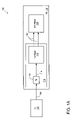
- FIG. 1A is a block diagram of an optical communication system according to an embodiment of the present invention.
- FIG. 1B is a graph of the light intensity of an exemplary light signal sent by the transmitter over a period of time
- FIG. 1C is a graph of the signal strength of an exemplary electrical signal produced by a photo-diode over a period of time
- FIG. 1D is a graph of the signal strength of exemplary differential signals produced by a first stage circuit over a period of time
- FIG. 2A is a diagram of a signal detector circuit in accordance with the present invention.
- FIG. 2B is a graph of the voltage at points A L and B L of the signal detector circuit of FIG. 2A ;
- FIG. 2C is a graph of the voltage at points A R and B R of the signal detector circuit of FIG. 2A ;
- FIG. 2D is a graph of the voltage across a first resistor of the signal detector circuit of FIG. 2A ; circuit of FIG. 2A ;
- FIG. 2F is a diagram of another signal detector circuit in accordance with the present invention.
- FIG. 2G is a graph of the voltage across the second resistor of the signal detector circuit of FIG. 2F .
- FIG. 1A shows a block diagram of an optical communication system 100 according to one embodiment of the present invention.
- the communication system 100 includes an optoelectronic transmitter/transceiver 102 that transmits a light signal 104 with an associated frequency and light intensity.
- the transmitter 102 typically includes a laser and optics (not illustrated) to transmit the light signal 104 .
- a light intensity graph 106 included in FIG. 1B shows the light intensity of an exemplary light signal 104 sent by the transmitter 102 over a period of time.
- the light intensity corresponds to the voltage of the light signal 104 .
- the peak-to-peak amplitude or signal strength of the light signal 104 is denoted on the light intensity graph 106 by the symbol 2 ⁇ .
- the communication system 100 also includes an optoelectronic receiver/transceiver 110 that receives the light signal 104 from the transmitter 102 .
- the receiver 110 contains a photo-diode 112 , a first stage circuit 118 (e.g., a Pre-Amplifier Circuit), and a second stage circuit 124 (e.g., a Post-Amplifier Circuit).
- the photo-diode 112 and the first stage circuit 118 are integrated into a Transistor Outline (TO) package 119 , which is typically part of the optoelectronic receiver/transceiver 110 .
- TO Transistor Outline
- the photo-diode 112 receives the light signal 104 from the transmitter 102 and converts it to an electrical signal 114 .
- the electrical signal 114 has an associated signal strength corresponding to the voltage of the electrical signal 114 .
- a signal intensity graph 116 included in FIG. 1C shows the signal strength of an exemplary electrical signal 114 produced by the photo-diode 112 over a period of time.
- the peak-to-peak amplitude or signal strength of the electrical signal 114 is denoted on the signal intensity graph 116 as 2 ⁇ .′
- the signal strength 2 ⁇ ′ of the electrical signal 114 is proportional to the signal strength 2 ⁇ of the light signal 104 . This proportionality is a function of the photo diode's 112 scaling or loss factors.
- the first stage circuit 118 receives the electrical signal 114 from the photodiode 112 and produces amplified differential signals 120 .
- the amplified differential signals 120 consist of a positive pre-amplifier output and a negative preamplifier output.
- the amplified differential signals 120 have a signal strength that corresponds to the voltage thereof.
- a signal intensity graph 122 included in FIG. 1D shows the signal strength of exemplary differential signals 120 produced by the first stage circuit 118 over a period of time.
- the positive pre-amplifier output corresponds to the dashed line and the negative pre-amplifier output corresponds to the solid line.
- the voltage of the positive pre-amplifier output is at a maximum (e.g., at M ⁇ ′) when the voltage of the negative pre-amplifier output is at a minimum (e.g., at ⁇ M ⁇ ′) and vice versa.
- the amplified differential signals 120 are nominally equal in amplitude, but 180 degrees out of phase.
- the peak-to-peak amplitude or signal strength of the differential signals 120 is represented on the signal intensity graph 122 as 2M ⁇ ′, where M corresponds to the amplification factor of the first stage circuit 118 .
- the signal strength 2 ⁇ of the light signal 104 may be derived from the signal strength 2M ⁇ ′ of the differential signals 120 by first determining the signal strength 2 ⁇ ′ of the electrical signal 114 using the amplification factor M of the first stage circuit 118 and then determining the signal strength 2 ⁇ of the light signal 104 using the scaling or loss factors of the photo diode 112 .
- the second stage circuit 124 receives the differential signals 120 from the first stage circuit 118 for further processing.
- the present invention provides particular circuit designs for use as part of the second stage circuit 124 to determine the signal strength 2M ⁇ ′ of the differential signals 120 .
- FIG. 2A shows a general circuit layout for a signal detector circuit 200 for use in or as the second stage circuit 124 of FIG. 1A in accordance with an embodiment of the present invention.
- the signal detector circuit 200 includes a first resistor 206 with a resistance value of R1, a second resistor 208 with a resistance value of R2, a first left transistor 202 (i.e., a first transistor positioned to the left of the first resistor 206 in FIG. 2A ), a first right transistor 204 (i.e., a first transistor positioned to the right of the first resistor 206 in FIG.
- a first left current source 212 producing a current I 1 L
- a first right current source 214 producing a current I 1 R
- a second left transistor 216 producing a current I 1 R
- a second right current source 214 producing a current I 1 R
- a third left resistor 220 with a resistance value of R3 L
- a third right resistor 222 with a resistance value of R3 R
- a fourth left resistor 224 with a resistance value of R4 L
- a fourth right resistor 226 with a resistance value of R4 R
- a third left transistor 228 , a third right transistor 230
- a fifth left resistor 232 with a resistance value of R5 L
- a fifth right resistor 234 with a resistance value of R5 R
- a sixth left resistor 236 with a resistance value of R6 L
- a sixth right resistor 238 with a resistance value of R6 R
- a second left current source 240 producing a current I 2 L
- the emitter terminal of the first left transistor 202 is coupled to the first resistor 206 and the first left current source 212 .
- the collector terminal of the first left transistor 202 is coupled to the source terminal of the second left transistor 216 , the source terminal of the third left transistor 228 , and the second left current source 240 .
- the base terminal of the first left transistor 202 is coupled to the first stage circuit 118 ( FIG. 1A ) and receives a first of the differential signals 120 produced by the first stage circuit 118 .
- the gate terminal of the second left transistor 216 is coupled to the third and fourth left resistors 220 , 224 .
- the third left resistor 220 is also coupled to a power source and the fourth left resistor 224 is also coupled to circuit ground.
- the drain terminal of the second left transistor 216 is coupled to the second resistor 208 and the drain terminal of the second right transistor 218 .
- the second resistor 208 is also coupled to circuit ground.
- the gate terminal of the third left transistor 228 is coupled to the fifth and sixth left resistors 232 , 236 .
- the fifth left resistor 232 is also coupled to a power source and the sixth left resistor 236 is also coupled to circuit ground.
- the drain terminal of the third left transistor 228 is coupled to a power source.
- the source terminal of the third left transistor 228 is coupled to the source terminal of the second left transistor 216 and coupled to the second left current source 240 .
- the emitter terminal of the first right transistor 204 is coupled to the first resistor 206 and the first right current source 214 .
- the collector terminal of the first right transistor 204 is coupled to the source terminal of the second right transistor 218 , the source terminal of the third right transistor 230 , and the second right current source 242 .
- the base terminal of the first right transistor 204 is coupled to the first stage circuit 118 ( FIG. 1A ) and receives a second of the differential signals 120 produced by the first stage circuit 118 .
- the gate terminal of the second right transistor 218 is coupled to the third and fourth right resistors 222 , 226 .
- the third right resistor 222 is also coupled to a power source and the fourth right resistor 226 is also coupled to circuit ground.
- the drain terminal of the second right transistor 218 is coupled to the second resistor 208 and the drain terminal of the second left transistor 216 .
- the gate terminal of the third right transistor 230 is coupled to the fifth and sixth right resistors 234 , 238 .
- the fifth right resistor 234 is also coupled to a power source and the sixth right resistor 238 is also coupled to circuit ground.
- the drain terminal of the third right transistor 230 is coupled to a power source.
- the source terminal of the third right transistor 230 is coupled to the source terminal of the second right transistor 218 and coupled to the second right current source 242 .
- the first left transistor 202 and first right transistor 204 are bipolar junction transistors (BJTs) and the second left transistor 216 , second right transistor 218 , third left transistor 228 , and third right transistor 230 are field effect transistors (FETs).
- BJTs bipolar junction transistors
- FETs field effect transistors
- the current I EL which is the current flowing out of the emitter of the first left transistor 202
- the current I CL which is the current flowing into the collector of the first left transistor 202
- the current I EL is substantially equal to the current I CL because the current I CL is much greater than the current flowing into the base terminal of the first left transistor 202 .
- the current I ER which is the current flowing out of the emitter of the first right transistor 204
- the current I CR which is the current flowing into the collector of the first left transistor 204
- the current I CR is much greater than the current flowing into the base terminal of the first right transistor 204 .
- the signal detector circuit 200 is preferably configured such that the power sources, resistors, and circuit ground connected directly or indirectly to the gate terminals of the second and third left transistors 216 , 228 and the second and third right transistors 218 , 230 , respectively, turn these transistors on and off (e.g., enable the flow of current through the source and drain terminals of these transistors) instead of controlling the flow of current through the source and drain terminals of these transistors so that it corresponds to the voltage at the respective gate terminals of these transistors. So significant current flows through the source and drain terminals of these transistors only when “pulled” or “pushed” by other aspects of the signal detector circuit 200 .
- the arrows on the source terminals of the second and third left transistors 216 , 228 and the second and right transistors 218 , 230 indicate the only direction in which current may flow through these terminals. So if the amplitude of the current I CL is less than the amplitude of the current I 2 L , which is produced by the second left current source 240 , current flows into and out of the source and drain terminals, respectively, of the second left transistor 216 . Conversely, if the amplitude of the current I CL is greater than the amplitude of the current I 2 L , current flows from the source terminal of the third left transistor 228 .
- the amplitude of the current I CR is less than the amplitude of the current I 2 R , which is produced by the second right current source 242 , current flows into and out of the source and drain terminals, respectively, of the second right transistor 218 . Conversely, if the amplitude of the current I CR is greater than the amplitude of the current I 2 R , current flows from the source terminal of the third right transistor 230 .
- the voltage drop across the respective collector and emitter terminals of the first left and right transistors 202 , 204 is preferably greater than or equal to 0.5 volts. This ensures that the first left and right transistors 202 , 204 are turned on.
- a voltage drop greater than or equal to 0.5 volts is preferably accomplished with standard transistor biasing techniques known in the art.
- the amplitude of the current produced by the constant current sources 212 , 214 , 240 , 242 and the resistive value of the first resistor 206 are preferably selected so that the current that flows through the collector and emitter terminals of the first left and right transistors 202 , 204 is only a function of the voltage drop across the first resistor 206 and not the gain of these transistors.
- the base terminal of the first left transistor 202 receives one of the differential signals 120 produced by the first stage circuit 118 and the base terminal of the first right transistor 204 receives the other differential signal 120 produced by the first stage circuit 118 .
- the voltages received at the base terminals of the first left transistor 202 and the first right transistor 204 are nominally equal in amplitude, but 180 degrees out of phase.
- K is preferably a DC voltage offset sufficiently high enough to at least ensure that the first left transistor 202 and the first right transistor 204 are turned on regardless of the value of the differential signals 120 . More specifically, the offset voltage across the base and emitter of a typical transistor (e.g., the first left transistor 202 and the first right transistor 204 ) is usually 0.6 or 0.7 volts.
- the voltage at point A L over time is shown in FIG. 2B as a solid line.
- the differential signal 120 received at point A L has a peak-to-peak amplitude of 2M ⁇ ′ and fluctuates between a maximum voltage of K+M ⁇ ′ and a minimum voltage of K ⁇ M ⁇ ′.
- the voltage at point A R over time is shown in FIG. 2C as a solid line.
- the differential signal 120 received at point A R also has a peak-to-peak amplitude of 2M ⁇ ′ and fluctuates between a maximum voltage of K+M ⁇ ′ and a minimum voltage of K ⁇ M ⁇ ′.
- the peak-to-peak voltage at point B L over time is the same as the voltage at point A L but offset by 0.7V.
- the peak-to-peak voltage at B R over time is the same as the voltage at A R but offset by 0.7V.
- the voltage V R1 across the first resistor 206 is equal to (K+M ⁇ ′ ⁇ 0.7V) ⁇ (K ⁇ M ⁇ ′ ⁇ 0.7V), which is equal to 2M ⁇ ′.
- the voltage V R1 across the first resistor 206 is equal to (K ⁇ M ⁇ ′ ⁇ 0.7V) ⁇ (K+M ⁇ ′ ⁇ 0.7V), which is equal to ⁇ 2M ⁇ ′.
- the voltage V R1 over time is shown in FIG.
- the current I R1 flowing through the first resistor 206 therefore, is equal to (V R1/R1 ) and varies from (2M ⁇ ′/R1) to ( ⁇ 2M ⁇ ′/R1) over time.
- the value of the current I EL flowing out of the emitter terminal of the first left transistor 202 is equal to the current I 1 L produced by the first left current source 212 plus the current I R1 flowing through the first resistor 206 . Therefore, when the voltage at point A L is at a maximum voltage of K+M ⁇ ′, the current I EL is equal to (I 1 L +2M ⁇ ′/R1). And when the voltage at point A L is at a minimum voltage of K ⁇ M ⁇ ′, the current I EL is equal to (I 1 L +( ⁇ 2M ⁇ ′/R1)).
- the first and second left current sources 212 , 240 are preferably configured to ensure that 1) a positive current always flows through the first left transistor 202 , a requirement for the first left transistor 202 to remain on and 2) a current proportional to the differential signals 120 flows through the second left transistor 216 when the current I 2 L exceeds the current I CL . To do so, these current sources preferably each produce a current greater than (2M ⁇ ′/R1).
- the value of the current I ER flowing out of the emitter terminal of the first right transistor 204 is equal to the current I 1 R produced by the first right current source 214 minus the current I R1 flowing through the first resistor 206 . Therefore, when the voltage at point A R is at a minimum voltage of K ⁇ M ⁇ ′, the current I ER is equal to (I 1 R +( ⁇ 2M ⁇ ′/R1)). And when the voltage at point A R is at a maximum voltage of K+M ⁇ ′, the current I ER is equal to (I 1 R +2M ⁇ ′/R1)).
- current I CR is (I 1 R +2M ⁇ ′/R1). If the current I 2 R produced by the second right current source 242 is equal to I 1 R , a current equal to (2M ⁇ ′/R1) is pulled from the third right transistor 230 and no significant amount of current flows into the second right transistor 218 .
- the first and second right current sources 214 , 242 are preferably configured to ensure that 1) a positive current always flows through the first right transistor 204 , a requirement for the first right transistor 204 to remain on and 2) a current proportional to the differential signals 120 flows through the second right transistor 218 when the current I 2 R exceeds the current I CR . To do so, these current sources preferably each produce a current greater than (2M ⁇ ′/R1).
- the voltage across the second resistor 208 (i.e., the voltage V R2 ) is equal to (2M ⁇ ′/R1)*R2.
- the ideal output of the signal detector circuit 200 or the voltage drop, V R2 , across the second resistor 208 is illustrated in FIG. 2E .
- the signal strength 2M ⁇ ′ of the differential signals 120 can be determined from the voltage V R2 across the second resistor 208 .
- the signal strength 2 ⁇ of the light signal 104 may be derived from the signal strength 2M ⁇ ′ of the differential signals 120 by first determining the signal strength 2 ⁇ ′ of the electrical signal 114 using the amplification factor M of the first stage circuit 118 and then determining the signal strength 2 ⁇ of the light signal 104 using the scaling or loss factors of the photo diode 112 .
- the voltage drop across the second resistor 208 is input to, for example, an A/D converter 252 —as illustrated in FIG. 2F .
- the output of the A/D converter may then be read by a microprocessor 254 or other device.
- the result can thus be read by an external system via a standard transceiver interface.
- output of the signal detector circuit 200 illustrated in FIG. 2E is an idealized output.
- the voltage wave forms illustrated in FIGS. 2B-2D are not perfect square waves. Instead, a certain amount of time is required for the voltages to swing from a maximum amplitude to a minimum amplitude and vice versa.
- a capacitor 250 may be included in some embodiments of the present invention in parallel with the second resistor 208 , as also illustrated in FIG. 2F , in order to smooth out the wave form illustrated in FIG. 2G .
- the period of the differential signals is known so that the voltage V R2 is sampled only during periods of stability, which correspond to when the voltages at the base terminals of one or the other of the first left transistor 202 and the first right transistor 204 is equal to the minimum voltage of K ⁇ M ⁇ ′.
- the present invention represents an improvement over prior art signal detector circuits. This is due in part to the fact that the present invention does not rely upon the gain of the transistors included therein. Instead, the transistors are merely turned on to enable the flow of current. And the current across the second resistor 208 results from current across the first resistor 206 , which is a function of the relative values of the differential signals 120 , and the fact that current flows through transistors in only one direction regardless of temperature or method of manufacture. And any offset voltage variations of the transistors illustrated in FIG. 2A or FIG. 2F due to temperature are largely offset by equal changes in corresponding transistors (e.g., a change in the offset voltage of the first left transistor 202 is largely offset by an equal change in the offset voltage of the first right transistor 204 ).
Landscapes
- Physics & Mathematics (AREA)
- Electromagnetism (AREA)
- Engineering & Computer Science (AREA)
- Computer Networks & Wireless Communication (AREA)
- Signal Processing (AREA)
- Amplifiers (AREA)
Abstract
Description
Claims (8)
Priority Applications (1)
| Application Number | Priority Date | Filing Date | Title |
|---|---|---|---|
| US11/068,284 US7470884B2 (en) | 2002-02-14 | 2005-02-28 | Signal strength detection circuits for high speed optical electronics |
Applications Claiming Priority (3)
| Application Number | Priority Date | Filing Date | Title |
|---|---|---|---|
| US35760802P | 2002-02-14 | 2002-02-14 | |
| US10/285,083 US7038187B2 (en) | 2002-02-14 | 2002-10-31 | Circuit for measuring photo-current level in fiber optic links |
| US11/068,284 US7470884B2 (en) | 2002-02-14 | 2005-02-28 | Signal strength detection circuits for high speed optical electronics |
Related Parent Applications (1)
| Application Number | Title | Priority Date | Filing Date |
|---|---|---|---|
| US10/285,083 Division US7038187B2 (en) | 2002-02-14 | 2002-10-31 | Circuit for measuring photo-current level in fiber optic links |
Publications (2)
| Publication Number | Publication Date |
|---|---|
| US20050151063A1 US20050151063A1 (en) | 2005-07-14 |
| US7470884B2 true US7470884B2 (en) | 2008-12-30 |
Family
ID=27668561
Family Applications (3)
| Application Number | Title | Priority Date | Filing Date |
|---|---|---|---|
| US10/285,083 Expired - Fee Related US7038187B2 (en) | 2002-02-14 | 2002-10-31 | Circuit for measuring photo-current level in fiber optic links |
| US11/068,284 Expired - Lifetime US7470884B2 (en) | 2002-02-14 | 2005-02-28 | Signal strength detection circuits for high speed optical electronics |
| US11/068,657 Expired - Fee Related US6965103B2 (en) | 2002-02-14 | 2005-02-28 | Signal strength detection circuits for high speed optical electronics |
Family Applications Before (1)
| Application Number | Title | Priority Date | Filing Date |
|---|---|---|---|
| US10/285,083 Expired - Fee Related US7038187B2 (en) | 2002-02-14 | 2002-10-31 | Circuit for measuring photo-current level in fiber optic links |
Family Applications After (1)
| Application Number | Title | Priority Date | Filing Date |
|---|---|---|---|
| US11/068,657 Expired - Fee Related US6965103B2 (en) | 2002-02-14 | 2005-02-28 | Signal strength detection circuits for high speed optical electronics |
Country Status (1)
| Country | Link |
|---|---|
| US (3) | US7038187B2 (en) |
Families Citing this family (4)
| Publication number | Priority date | Publication date | Assignee | Title |
|---|---|---|---|---|
| JP4328660B2 (en) * | 2004-04-15 | 2009-09-09 | 富士重工業株式会社 | Aircraft automatic take-off device, automatic landing device, automatic take-off and landing device, aircraft automatic take-off method, automatic landing method, and automatic take-off and landing method |
| WO2019191482A1 (en) | 2018-03-30 | 2019-10-03 | Becton, Dickinson And Company | Water-soluble polymeric dyes having pendant chromophores |
| JP7416729B2 (en) | 2018-06-19 | 2024-01-17 | ベクトン・ディキンソン・アンド・カンパニー | Variable multiplexing switch, system, and method of use for detector arrays |
| EP3814748A4 (en) * | 2018-06-28 | 2022-03-30 | Becton, Dickinson and Company | Integrated pre-amplification light detection systems and methods of use thereof |
Citations (4)
| Publication number | Priority date | Publication date | Assignee | Title |
|---|---|---|---|---|
| US5237526A (en) * | 1991-08-29 | 1993-08-17 | The United States Of America As Represented By The Secretary Of The Navy | High speed electronic analog computers using low-gain amplifiers |
| US6366165B1 (en) * | 1998-11-16 | 2002-04-02 | U.S. Philips Corporation | Amplifier with stabilization means |
| US6528777B2 (en) * | 2001-01-16 | 2003-03-04 | International Business Machines Corporation | Optical power meter derived from common-mode voltage of optical transimpedance amplifier |
| US6855920B2 (en) * | 2002-02-14 | 2005-02-15 | Finisar Corporation | Signal strength detection in high-speed optical electronics |
Family Cites Families (1)
| Publication number | Priority date | Publication date | Assignee | Title |
|---|---|---|---|---|
| JP2503837B2 (en) * | 1992-07-16 | 1996-06-05 | 日本電気株式会社 | Digital optical receiver circuit and preamplifier circuit in digital optical receiver circuit |
-
2002
- 2002-10-31 US US10/285,083 patent/US7038187B2/en not_active Expired - Fee Related
-
2005
- 2005-02-28 US US11/068,284 patent/US7470884B2/en not_active Expired - Lifetime
- 2005-02-28 US US11/068,657 patent/US6965103B2/en not_active Expired - Fee Related
Patent Citations (4)
| Publication number | Priority date | Publication date | Assignee | Title |
|---|---|---|---|---|
| US5237526A (en) * | 1991-08-29 | 1993-08-17 | The United States Of America As Represented By The Secretary Of The Navy | High speed electronic analog computers using low-gain amplifiers |
| US6366165B1 (en) * | 1998-11-16 | 2002-04-02 | U.S. Philips Corporation | Amplifier with stabilization means |
| US6528777B2 (en) * | 2001-01-16 | 2003-03-04 | International Business Machines Corporation | Optical power meter derived from common-mode voltage of optical transimpedance amplifier |
| US6855920B2 (en) * | 2002-02-14 | 2005-02-15 | Finisar Corporation | Signal strength detection in high-speed optical electronics |
Non-Patent Citations (1)
| Title |
|---|
| U.S. Appl. No. 11/068,657, filed Feb. 28, 2005 entitled "Signal Strength Detection Circuits for High Speed Optical Electronics.". |
Also Published As
| Publication number | Publication date |
|---|---|
| US20030150978A1 (en) | 2003-08-14 |
| US20050151063A1 (en) | 2005-07-14 |
| US20050151064A1 (en) | 2005-07-14 |
| US7038187B2 (en) | 2006-05-02 |
| US6965103B2 (en) | 2005-11-15 |
Similar Documents
| Publication | Publication Date | Title |
|---|---|---|
| US20040222360A1 (en) | Method and apparatus for monitoring a photo-detector | |
| JPS62145938A (en) | Photodetector | |
| JPH118522A (en) | Digital receiving circuit | |
| US8901475B1 (en) | Avalanche photodiode biasing system including a current mirror, voltage-to-current converter circuit, and a feedback path sensing an avalanche photodiode voltage | |
| US7439480B2 (en) | Regulated current mirror | |
| US7470884B2 (en) | Signal strength detection circuits for high speed optical electronics | |
| US6952005B2 (en) | Optical receiver circuit | |
| US9882638B2 (en) | Optical receiver signal strength indicator (RSSI) circuit having a variable supply voltage filter impedance | |
| US5224112A (en) | Semiconductor laser device driving circuit | |
| US6919716B1 (en) | Precision avalanche photodiode current monitor | |
| US7193478B2 (en) | Signal transmission in opto-electronic devices by moving the quiescent component of a differential signal | |
| US11411542B2 (en) | Transimpedance amplifier circuit | |
| US20070104493A1 (en) | Optical receiver preamplifier | |
| US6566955B1 (en) | High bandwidth transresistance amplifier | |
| US7612322B2 (en) | Temperature-compensated high dynamic range optical receiver | |
| US6956195B2 (en) | Photoelectric current and voltage converting circuit | |
| JP4032531B2 (en) | Optical receiver | |
| US6356065B1 (en) | Current-voltage converter with changeable threshold based on peak inputted current | |
| US6855920B2 (en) | Signal strength detection in high-speed optical electronics | |
| EP1081858A2 (en) | Current-voltage converter | |
| JPH0315859B2 (en) | ||
| US6756851B2 (en) | Transimpedance amplifier | |
| US20030117121A1 (en) | High-side current-sense circuit for precision application | |
| CN217034616U (en) | Laser instrument current control circuit based on V-I conversion | |
| JP7073609B2 (en) | Optical receiver and power monitoring method for optical receiver |
Legal Events
| Date | Code | Title | Description |
|---|---|---|---|
| STCF | Information on status: patent grant |
Free format text: PATENTED CASE |
|
| CC | Certificate of correction | ||
| FPAY | Fee payment |
Year of fee payment: 4 |
|
| FPAY | Fee payment |
Year of fee payment: 8 |
|
| AS | Assignment |
Owner name: FINISAR CORPORATION, CALIFORNIA Free format text: ASSIGNMENT OF ASSIGNORS INTEREST;ASSIGNOR:SHAPIRO, PHIL;REEL/FRAME:040406/0046 Effective date: 20021025 |
|
| AS | Assignment |
Owner name: BANK OF AMERICA, N.A., AS ADMINISTRATIVE AGENT, NO Free format text: NOTICE OF GRANT OF SECURITY INTEREST IN PATENTS;ASSIGNORS:II-VI INCORPORATED;MARLOW INDUSTRIES, INC.;EPIWORKS, INC.;AND OTHERS;REEL/FRAME:050484/0204 Effective date: 20190924 Owner name: BANK OF AMERICA, N.A., AS ADMINISTRATIVE AGENT, NORTH CAROLINA Free format text: NOTICE OF GRANT OF SECURITY INTEREST IN PATENTS;ASSIGNORS:II-VI INCORPORATED;MARLOW INDUSTRIES, INC.;EPIWORKS, INC.;AND OTHERS;REEL/FRAME:050484/0204 Effective date: 20190924 |
|
| AS | Assignment |
Owner name: II-VI DELAWARE, INC., DELAWARE Free format text: ASSIGNMENT OF ASSIGNORS INTEREST;ASSIGNOR:FINISAR CORPORATION;REEL/FRAME:052286/0001 Effective date: 20190924 |
|
| MAFP | Maintenance fee payment |
Free format text: PAYMENT OF MAINTENANCE FEE, 12TH YEAR, LARGE ENTITY (ORIGINAL EVENT CODE: M1553); ENTITY STATUS OF PATENT OWNER: LARGE ENTITY Year of fee payment: 12 |
|
| AS | Assignment |
Owner name: JPMORGAN CHASE BANK, N.A., AS COLLATERAL AGENT, NEW YORK Free format text: SECURITY INTEREST;ASSIGNORS:II-VI INCORPORATED;II-VI DELAWARE, INC.;M CUBED TECHNOLOGIES, INC.;AND OTHERS;REEL/FRAME:060562/0254 Effective date: 20220701 |
|
| AS | Assignment |
Owner name: PHOTOP TECHNOLOGIES, INC., CALIFORNIA Free format text: PATENT RELEASE AND REASSIGNMENT;ASSIGNOR:BANK OF AMERICA, N.A., AS ADMINISTRATIVE AGENT;REEL/FRAME:060574/0001 Effective date: 20220701 Owner name: II-VI OPTOELECTRONIC DEVICES, INC., NEW JERSEY Free format text: PATENT RELEASE AND REASSIGNMENT;ASSIGNOR:BANK OF AMERICA, N.A., AS ADMINISTRATIVE AGENT;REEL/FRAME:060574/0001 Effective date: 20220701 Owner name: II-VI DELAWARE, INC., PENNSYLVANIA Free format text: PATENT RELEASE AND REASSIGNMENT;ASSIGNOR:BANK OF AMERICA, N.A., AS ADMINISTRATIVE AGENT;REEL/FRAME:060574/0001 Effective date: 20220701 Owner name: II-VI PHOTONICS (US), INC., MASSACHUSETTS Free format text: PATENT RELEASE AND REASSIGNMENT;ASSIGNOR:BANK OF AMERICA, N.A., AS ADMINISTRATIVE AGENT;REEL/FRAME:060574/0001 Effective date: 20220701 Owner name: M CUBED TECHNOLOGIES, INC., CONNECTICUT Free format text: PATENT RELEASE AND REASSIGNMENT;ASSIGNOR:BANK OF AMERICA, N.A., AS ADMINISTRATIVE AGENT;REEL/FRAME:060574/0001 Effective date: 20220701 Owner name: II-VI OPTICAL SYSTEMS, INC., CALIFORNIA Free format text: PATENT RELEASE AND REASSIGNMENT;ASSIGNOR:BANK OF AMERICA, N.A., AS ADMINISTRATIVE AGENT;REEL/FRAME:060574/0001 Effective date: 20220701 Owner name: FINISAR CORPORATION, CALIFORNIA Free format text: PATENT RELEASE AND REASSIGNMENT;ASSIGNOR:BANK OF AMERICA, N.A., AS ADMINISTRATIVE AGENT;REEL/FRAME:060574/0001 Effective date: 20220701 Owner name: OPTIUM CORPORATION, CALIFORNIA Free format text: PATENT RELEASE AND REASSIGNMENT;ASSIGNOR:BANK OF AMERICA, N.A., AS ADMINISTRATIVE AGENT;REEL/FRAME:060574/0001 Effective date: 20220701 Owner name: COADNA PHOTONICS, INC., PENNSYLVANIA Free format text: PATENT RELEASE AND REASSIGNMENT;ASSIGNOR:BANK OF AMERICA, N.A., AS ADMINISTRATIVE AGENT;REEL/FRAME:060574/0001 Effective date: 20220701 Owner name: KAILIGHT PHOTONICS, INC., CALIFORNIA Free format text: PATENT RELEASE AND REASSIGNMENT;ASSIGNOR:BANK OF AMERICA, N.A., AS ADMINISTRATIVE AGENT;REEL/FRAME:060574/0001 Effective date: 20220701 Owner name: LIGHTSMYTH TECHNOLOGIES, INC., OREGON Free format text: PATENT RELEASE AND REASSIGNMENT;ASSIGNOR:BANK OF AMERICA, N.A., AS ADMINISTRATIVE AGENT;REEL/FRAME:060574/0001 Effective date: 20220701 Owner name: EPIWORKS, INC., ILLINOIS Free format text: PATENT RELEASE AND REASSIGNMENT;ASSIGNOR:BANK OF AMERICA, N.A., AS ADMINISTRATIVE AGENT;REEL/FRAME:060574/0001 Effective date: 20220701 Owner name: MARLOW INDUSTRIES, INC., TEXAS Free format text: PATENT RELEASE AND REASSIGNMENT;ASSIGNOR:BANK OF AMERICA, N.A., AS ADMINISTRATIVE AGENT;REEL/FRAME:060574/0001 Effective date: 20220701 Owner name: II-VI INCORPORATED, PENNSYLVANIA Free format text: PATENT RELEASE AND REASSIGNMENT;ASSIGNOR:BANK OF AMERICA, N.A., AS ADMINISTRATIVE AGENT;REEL/FRAME:060574/0001 Effective date: 20220701 |