US7411818B1 - Programmable fuse/non-volatile memory structures using externally heated phase change material - Google Patents
Programmable fuse/non-volatile memory structures using externally heated phase change material Download PDFInfo
- Publication number
- US7411818B1 US7411818B1 US11/672,110 US67211007A US7411818B1 US 7411818 B1 US7411818 B1 US 7411818B1 US 67211007 A US67211007 A US 67211007A US 7411818 B1 US7411818 B1 US 7411818B1
- Authority
- US
- United States
- Prior art keywords
- phase change
- silicide
- change material
- pcm
- wire structure
- Prior art date
- Legal status (The legal status is an assumption and is not a legal conclusion. Google has not performed a legal analysis and makes no representation as to the accuracy of the status listed.)
- Active
Links
- 239000012782 phase change material Substances 0.000 title claims abstract description 92
- 239000004065 semiconductor Substances 0.000 claims abstract description 7
- 229910021332 silicide Inorganic materials 0.000 claims description 42
- FVBUAEGBCNSCDD-UHFFFAOYSA-N silicide(4-) Chemical compound [Si-4] FVBUAEGBCNSCDD-UHFFFAOYSA-N 0.000 claims description 38
- 238000000034 method Methods 0.000 claims description 24
- 229910021420 polycrystalline silicon Inorganic materials 0.000 claims description 19
- 239000000463 material Substances 0.000 claims description 18
- 229920005591 polysilicon Polymers 0.000 claims description 18
- 229910052751 metal Inorganic materials 0.000 claims description 14
- 239000002184 metal Substances 0.000 claims description 14
- 239000000758 substrate Substances 0.000 claims description 6
- 239000000956 alloy Substances 0.000 claims description 3
- 238000000059 patterning Methods 0.000 claims description 3
- 229910052691 Erbium Inorganic materials 0.000 claims description 2
- 229910052769 Ytterbium Inorganic materials 0.000 claims description 2
- 229910017052 cobalt Inorganic materials 0.000 claims description 2
- 239000010941 cobalt Substances 0.000 claims description 2
- GUTLYIVDDKVIGB-UHFFFAOYSA-N cobalt atom Chemical compound [Co] GUTLYIVDDKVIGB-UHFFFAOYSA-N 0.000 claims description 2
- UYAHIZSMUZPPFV-UHFFFAOYSA-N erbium Chemical compound [Er] UYAHIZSMUZPPFV-UHFFFAOYSA-N 0.000 claims description 2
- 229910052715 tantalum Inorganic materials 0.000 claims description 2
- GUVRBAGPIYLISA-UHFFFAOYSA-N tantalum atom Chemical compound [Ta] GUVRBAGPIYLISA-UHFFFAOYSA-N 0.000 claims description 2
- NAWDYIZEMPQZHO-UHFFFAOYSA-N ytterbium Chemical compound [Yb] NAWDYIZEMPQZHO-UHFFFAOYSA-N 0.000 claims description 2
- ZXEYZECDXFPJRJ-UHFFFAOYSA-N $l^{3}-silane;platinum Chemical compound [SiH3].[Pt] ZXEYZECDXFPJRJ-UHFFFAOYSA-N 0.000 claims 1
- RUFLMLWJRZAWLJ-UHFFFAOYSA-N nickel silicide Chemical compound [Ni]=[Si]=[Ni] RUFLMLWJRZAWLJ-UHFFFAOYSA-N 0.000 claims 1
- 229910021334 nickel silicide Inorganic materials 0.000 claims 1
- 229910021339 platinum silicide Inorganic materials 0.000 claims 1
- 229910021341 titanium silicide Inorganic materials 0.000 claims 1
- WQJQOUPTWCFRMM-UHFFFAOYSA-N tungsten disilicide Chemical compound [Si]#[W]#[Si] WQJQOUPTWCFRMM-UHFFFAOYSA-N 0.000 claims 1
- 229910021342 tungsten silicide Inorganic materials 0.000 claims 1
- 210000004027 cell Anatomy 0.000 description 32
- 238000010438 heat treatment Methods 0.000 description 18
- 230000015572 biosynthetic process Effects 0.000 description 14
- 230000008569 process Effects 0.000 description 13
- 238000010791 quenching Methods 0.000 description 12
- 238000002844 melting Methods 0.000 description 9
- 230000008018 melting Effects 0.000 description 9
- PEUPIGGLJVUNEU-UHFFFAOYSA-N nickel silicon Chemical compound [Si].[Ni] PEUPIGGLJVUNEU-UHFFFAOYSA-N 0.000 description 8
- BASFCYQUMIYNBI-UHFFFAOYSA-N platinum Chemical compound [Pt] BASFCYQUMIYNBI-UHFFFAOYSA-N 0.000 description 8
- XUIMIQQOPSSXEZ-UHFFFAOYSA-N Silicon Chemical compound [Si] XUIMIQQOPSSXEZ-UHFFFAOYSA-N 0.000 description 7
- 229910052710 silicon Inorganic materials 0.000 description 7
- 239000010703 silicon Substances 0.000 description 7
- 238000003491 array Methods 0.000 description 6
- 229910052697 platinum Inorganic materials 0.000 description 6
- 238000004088 simulation Methods 0.000 description 6
- 239000004020 conductor Substances 0.000 description 5
- 238000000151 deposition Methods 0.000 description 5
- 230000008021 deposition Effects 0.000 description 5
- 238000010586 diagram Methods 0.000 description 5
- PXHVJJICTQNCMI-UHFFFAOYSA-N Nickel Chemical compound [Ni] PXHVJJICTQNCMI-UHFFFAOYSA-N 0.000 description 4
- VYPSYNLAJGMNEJ-UHFFFAOYSA-N Silicium dioxide Chemical compound O=[Si]=O VYPSYNLAJGMNEJ-UHFFFAOYSA-N 0.000 description 4
- 238000005516 engineering process Methods 0.000 description 4
- 238000005382 thermal cycling Methods 0.000 description 4
- 239000010936 titanium Substances 0.000 description 4
- 229910008479 TiSi2 Inorganic materials 0.000 description 3
- DFJQEGUNXWZVAH-UHFFFAOYSA-N bis($l^{2}-silanylidene)titanium Chemical compound [Si]=[Ti]=[Si] DFJQEGUNXWZVAH-UHFFFAOYSA-N 0.000 description 3
- 230000001419 dependent effect Effects 0.000 description 3
- 238000009792 diffusion process Methods 0.000 description 3
- 238000005530 etching Methods 0.000 description 3
- 229910052759 nickel Inorganic materials 0.000 description 3
- 229910018999 CoSi2 Inorganic materials 0.000 description 2
- KRHYYFGTRYWZRS-UHFFFAOYSA-N Fluorane Chemical compound F KRHYYFGTRYWZRS-UHFFFAOYSA-N 0.000 description 2
- VEXZGXHMUGYJMC-UHFFFAOYSA-N Hydrochloric acid Chemical compound Cl VEXZGXHMUGYJMC-UHFFFAOYSA-N 0.000 description 2
- 229910045601 alloy Inorganic materials 0.000 description 2
- 230000004888 barrier function Effects 0.000 description 2
- 230000008901 benefit Effects 0.000 description 2
- 150000004770 chalcogenides Chemical class 0.000 description 2
- 230000008859 change Effects 0.000 description 2
- 229910052681 coesite Inorganic materials 0.000 description 2
- 238000001816 cooling Methods 0.000 description 2
- 229910052906 cristobalite Inorganic materials 0.000 description 2
- 230000007423 decrease Effects 0.000 description 2
- 230000006870 function Effects 0.000 description 2
- 230000010354 integration Effects 0.000 description 2
- 238000001459 lithography Methods 0.000 description 2
- 239000000203 mixture Substances 0.000 description 2
- 238000005001 rutherford backscattering spectroscopy Methods 0.000 description 2
- 239000000377 silicon dioxide Substances 0.000 description 2
- 229910052682 stishovite Inorganic materials 0.000 description 2
- 210000000352 storage cell Anatomy 0.000 description 2
- 229910052905 tridymite Inorganic materials 0.000 description 2
- 229910012990 NiSi2 Inorganic materials 0.000 description 1
- GRYLNZFGIOXLOG-UHFFFAOYSA-N Nitric acid Chemical compound O[N+]([O-])=O GRYLNZFGIOXLOG-UHFFFAOYSA-N 0.000 description 1
- ATJFFYVFTNAWJD-UHFFFAOYSA-N Tin Chemical compound [Sn] ATJFFYVFTNAWJD-UHFFFAOYSA-N 0.000 description 1
- RTAQQCXQSZGOHL-UHFFFAOYSA-N Titanium Chemical compound [Ti] RTAQQCXQSZGOHL-UHFFFAOYSA-N 0.000 description 1
- 238000005054 agglomeration Methods 0.000 description 1
- 230000002776 aggregation Effects 0.000 description 1
- 238000004458 analytical method Methods 0.000 description 1
- QZPSXPBJTPJTSZ-UHFFFAOYSA-N aqua regia Chemical compound Cl.O[N+]([O-])=O QZPSXPBJTPJTSZ-UHFFFAOYSA-N 0.000 description 1
- QVGXLLKOCUKJST-UHFFFAOYSA-N atomic oxygen Chemical compound [O] QVGXLLKOCUKJST-UHFFFAOYSA-N 0.000 description 1
- 230000006399 behavior Effects 0.000 description 1
- 239000003990 capacitor Substances 0.000 description 1
- 238000006243 chemical reaction Methods 0.000 description 1
- 238000002425 crystallisation Methods 0.000 description 1
- 230000008025 crystallization Effects 0.000 description 1
- 230000001351 cycling effect Effects 0.000 description 1
- 230000007812 deficiency Effects 0.000 description 1
- 239000008367 deionised water Substances 0.000 description 1
- 229910021641 deionized water Inorganic materials 0.000 description 1
- 238000009826 distribution Methods 0.000 description 1
- 229910052735 hafnium Inorganic materials 0.000 description 1
- 238000000265 homogenisation Methods 0.000 description 1
- 239000012212 insulator Substances 0.000 description 1
- 238000002955 isolation Methods 0.000 description 1
- 238000004519 manufacturing process Methods 0.000 description 1
- 239000000155 melt Substances 0.000 description 1
- 230000005055 memory storage Effects 0.000 description 1
- 239000007769 metal material Substances 0.000 description 1
- 238000012986 modification Methods 0.000 description 1
- 230000004048 modification Effects 0.000 description 1
- 230000000877 morphologic effect Effects 0.000 description 1
- 229910017604 nitric acid Inorganic materials 0.000 description 1
- 150000004767 nitrides Chemical class 0.000 description 1
- 229910052760 oxygen Inorganic materials 0.000 description 1
- 239000001301 oxygen Substances 0.000 description 1
- 230000002093 peripheral effect Effects 0.000 description 1
- 230000000171 quenching effect Effects 0.000 description 1
- 239000003870 refractory metal Substances 0.000 description 1
- 230000000717 retained effect Effects 0.000 description 1
- 229910052702 rhenium Inorganic materials 0.000 description 1
- 229910052703 rhodium Inorganic materials 0.000 description 1
- -1 silicide metals Chemical class 0.000 description 1
- 238000004544 sputter deposition Methods 0.000 description 1
- 238000006467 substitution reaction Methods 0.000 description 1
- 229910052719 titanium Inorganic materials 0.000 description 1
- 238000009966 trimming Methods 0.000 description 1
- WFKWXMTUELFFGS-UHFFFAOYSA-N tungsten Chemical compound [W] WFKWXMTUELFFGS-UHFFFAOYSA-N 0.000 description 1
- 229910052721 tungsten Inorganic materials 0.000 description 1
- 239000010937 tungsten Substances 0.000 description 1
- XLYOFNOQVPJJNP-UHFFFAOYSA-N water Chemical compound O XLYOFNOQVPJJNP-UHFFFAOYSA-N 0.000 description 1
Images


Classifications
-
- G—PHYSICS
- G11—INFORMATION STORAGE
- G11C—STATIC STORES
- G11C11/00—Digital stores characterised by the use of particular electric or magnetic storage elements; Storage elements therefor
- G11C11/56—Digital stores characterised by the use of particular electric or magnetic storage elements; Storage elements therefor using storage elements with more than two stable states represented by steps, e.g. of voltage, current, phase, frequency
- G11C11/5678—Digital stores characterised by the use of particular electric or magnetic storage elements; Storage elements therefor using storage elements with more than two stable states represented by steps, e.g. of voltage, current, phase, frequency using amorphous/crystalline phase transition storage elements
-
- G—PHYSICS
- G11—INFORMATION STORAGE
- G11C—STATIC STORES
- G11C13/00—Digital stores characterised by the use of storage elements not covered by groups G11C11/00, G11C23/00, or G11C25/00
- G11C13/0002—Digital stores characterised by the use of storage elements not covered by groups G11C11/00, G11C23/00, or G11C25/00 using resistive RAM [RRAM] elements
- G11C13/0004—Digital stores characterised by the use of storage elements not covered by groups G11C11/00, G11C23/00, or G11C25/00 using resistive RAM [RRAM] elements comprising amorphous/crystalline phase transition cells
-
- G—PHYSICS
- G11—INFORMATION STORAGE
- G11C—STATIC STORES
- G11C13/00—Digital stores characterised by the use of storage elements not covered by groups G11C11/00, G11C23/00, or G11C25/00
- G11C13/0002—Digital stores characterised by the use of storage elements not covered by groups G11C11/00, G11C23/00, or G11C25/00 using resistive RAM [RRAM] elements
- G11C13/0021—Auxiliary circuits
- G11C13/0069—Writing or programming circuits or methods
-
- H—ELECTRICITY
- H10—SEMICONDUCTOR DEVICES; ELECTRIC SOLID-STATE DEVICES NOT OTHERWISE PROVIDED FOR
- H10B—ELECTRONIC MEMORY DEVICES
- H10B63/00—Resistance change memory devices, e.g. resistive RAM [ReRAM] devices
- H10B63/30—Resistance change memory devices, e.g. resistive RAM [ReRAM] devices comprising selection components having three or more electrodes, e.g. transistors
-
- H—ELECTRICITY
- H10—SEMICONDUCTOR DEVICES; ELECTRIC SOLID-STATE DEVICES NOT OTHERWISE PROVIDED FOR
- H10N—ELECTRIC SOLID-STATE DEVICES NOT OTHERWISE PROVIDED FOR
- H10N70/00—Solid-state devices having no potential barriers, and specially adapted for rectifying, amplifying, oscillating or switching
- H10N70/011—Manufacture or treatment of multistable switching devices
- H10N70/061—Shaping switching materials
- H10N70/063—Shaping switching materials by etching of pre-deposited switching material layers, e.g. lithography
-
- H—ELECTRICITY
- H10—SEMICONDUCTOR DEVICES; ELECTRIC SOLID-STATE DEVICES NOT OTHERWISE PROVIDED FOR
- H10N—ELECTRIC SOLID-STATE DEVICES NOT OTHERWISE PROVIDED FOR
- H10N70/00—Solid-state devices having no potential barriers, and specially adapted for rectifying, amplifying, oscillating or switching
- H10N70/20—Multistable switching devices, e.g. memristors
- H10N70/231—Multistable switching devices, e.g. memristors based on solid-state phase change, e.g. between amorphous and crystalline phases, Ovshinsky effect
-
- H—ELECTRICITY
- H10—SEMICONDUCTOR DEVICES; ELECTRIC SOLID-STATE DEVICES NOT OTHERWISE PROVIDED FOR
- H10N—ELECTRIC SOLID-STATE DEVICES NOT OTHERWISE PROVIDED FOR
- H10N70/00—Solid-state devices having no potential barriers, and specially adapted for rectifying, amplifying, oscillating or switching
- H10N70/20—Multistable switching devices, e.g. memristors
- H10N70/253—Multistable switching devices, e.g. memristors having three or more electrodes, e.g. transistor-like devices
-
- H—ELECTRICITY
- H10—SEMICONDUCTOR DEVICES; ELECTRIC SOLID-STATE DEVICES NOT OTHERWISE PROVIDED FOR
- H10N—ELECTRIC SOLID-STATE DEVICES NOT OTHERWISE PROVIDED FOR
- H10N70/00—Solid-state devices having no potential barriers, and specially adapted for rectifying, amplifying, oscillating or switching
- H10N70/801—Constructional details of multistable switching devices
- H10N70/821—Device geometry
-
- H—ELECTRICITY
- H10—SEMICONDUCTOR DEVICES; ELECTRIC SOLID-STATE DEVICES NOT OTHERWISE PROVIDED FOR
- H10N—ELECTRIC SOLID-STATE DEVICES NOT OTHERWISE PROVIDED FOR
- H10N70/00—Solid-state devices having no potential barriers, and specially adapted for rectifying, amplifying, oscillating or switching
- H10N70/801—Constructional details of multistable switching devices
- H10N70/861—Thermal details
- H10N70/8613—Heating or cooling means other than resistive heating electrodes, e.g. heater in parallel
-
- H—ELECTRICITY
- H10—SEMICONDUCTOR DEVICES; ELECTRIC SOLID-STATE DEVICES NOT OTHERWISE PROVIDED FOR
- H10N—ELECTRIC SOLID-STATE DEVICES NOT OTHERWISE PROVIDED FOR
- H10N70/00—Solid-state devices having no potential barriers, and specially adapted for rectifying, amplifying, oscillating or switching
- H10N70/801—Constructional details of multistable switching devices
- H10N70/881—Switching materials
- H10N70/882—Compounds of sulfur, selenium or tellurium, e.g. chalcogenides
- H10N70/8828—Tellurides, e.g. GeSbTe
-
- H—ELECTRICITY
- H10—SEMICONDUCTOR DEVICES; ELECTRIC SOLID-STATE DEVICES NOT OTHERWISE PROVIDED FOR
- H10N—ELECTRIC SOLID-STATE DEVICES NOT OTHERWISE PROVIDED FOR
- H10N70/00—Solid-state devices having no potential barriers, and specially adapted for rectifying, amplifying, oscillating or switching
- H10N70/801—Constructional details of multistable switching devices
- H10N70/881—Switching materials
- H10N70/884—Switching materials based on at least one element of group IIIA, IVA or VA, e.g. elemental or compound semiconductors
-
- G—PHYSICS
- G11—INFORMATION STORAGE
- G11C—STATIC STORES
- G11C13/00—Digital stores characterised by the use of storage elements not covered by groups G11C11/00, G11C23/00, or G11C25/00
- G11C13/0002—Digital stores characterised by the use of storage elements not covered by groups G11C11/00, G11C23/00, or G11C25/00 using resistive RAM [RRAM] elements
- G11C13/0021—Auxiliary circuits
- G11C13/0069—Writing or programming circuits or methods
- G11C2013/008—Write by generating heat in the surroundings of the memory material, e.g. thermowrite
Definitions
- the present invention relates generally to integrated circuit devices and, more particularly, to programmable fuse/non-volatile memory structures (and arrays) using externally heated phase change material.
- eFUSE Electrically programmable fuse
- IBM electromigration
- MIBM rupture
- Itel agglomeration
- the structure includes a heater element formed at a transistor gate level of a semiconductor device, the heater element further including a pair of electrodes connected by a thin wire structure with respect to the electrodes, the heater element configured to receive programming current passed therethrough, a layer of phase change material disposed on top of a portion of the thin wire structure, and sensing circuitry configured to sense the resistance of the phase change material.
- a non-volatile, programmable phase change material (PCM) memory array includes a plurality of memory cells arranged in rows and columns, with each memory cell comprising a heater element formed at a transistor gate level of a semiconductor device; the heater element further including a pair of electrodes connected by a thin wire structure with respect to the electrodes; the heater element configured to receive programming current passed therethrough; a layer of phase change material disposed on top of a portion of the thin wire structure; and sensing circuitry configured to sense the resistance of the phase change material.
- PCM phase change material
- a method of forming a programmable phase change material (PCM) structure includes forming a polysilicon layer over a semiconductor substrate, at a location corresponding to a transistor gate level of a semiconductor device; patterning the polysilicon layer so as to define a pair of electrodes and a thin wire structure connecting the electrodes; forming a silicide metal layer over the patterned polysilicon layer so as to define a heater element; and forming a layer of phase change material disposed on top of a portion of the thin wire structure of the heater element; wherein the portions of the silicide metal layer corresponding to the thin wire structure in contact with a portion of the phase change material are configured to selectively heat the portion of phase change material in a manner that programs the phase change material into one of a low resistance crystalline state and a high resistance amorphous state.
- PCM programmable phase change material
- FIG. 1 is a graph illustrating the exemplary thermal cycling operations of a phase change material
- FIGS. 2( a ) through 2 ( c ) are top and cross-sectional views of a programmable eFUSE device using an externally heated PCM, formed at the gate-level of device processing, in accordance with an embodiment of the invention
- FIGS. 3 and 4 are schematic diagrams illustrating the operation of the programmable eFUSE structure of FIG. 2 , in conjunction with an exemplary sensing circuit, in accordance with a further embodiment of the invention
- FIGS. 5( a ) through 5 ( c ) are top and cross-sectional views of a non-volatile memory cell using an externally heated PCM, formed at the gate-level of device processing, in accordance with a further embodiment of the invention.
- FIG. 6 is a schematic diagram illustrating the operation of the non-volatile memory cell of FIG. 5 ;
- FIG. 7( a ) is a schematic diagram illustrating an array of non-volatile memory cells using an externally heated PCM and associated sensing circuitry, in accordance with a further embodiment of the invention.
- FIGS. 7( b ) and 7 ( c ) are alternative embodiments of the sensing circuitry for an array of non-volatile memory cells
- FIG. 8( a ) is a graph illustrating the thermal conductivity properties of silicon as a function of temperature
- FIG. 8( b ) is a graph illustrating the relationship of heater resistance as a function of heater temperature
- FIGS. 9( a ) and 9 ( b ) illustrate temperature contours resulting from a PCM heating simulation of a device similar to the embodiment of FIG. 2 ;
- FIG. 10 is a table listing properties of various silicide metals used in CMOS processing.
- FIGS. 11 through 14 are top and cross-sectional views illustrating a more detailed, sequential description of an exemplary method of forming the device of FIG. 2 .
- eFUSE electrically reprogrammable fuse
- PCRAM Phase Change Random Access Memory
- PRAM Phase Change Random Access Memory
- Such devices may be advantageously integrated at a gate-level of device formation (i.e., at the front-end-of-line), thereby involving minimal changes to standard CMOS processing technology.
- phase change materials such as Ge—Sb—Te (GST) alloys
- GST Ge—Sb—Te
- Other compositions such as GeSb 4 , (including substitution/addition of other elements) are also possible for the phase change materials.
- Individual phase change elements are thus used as programmable eFUSEs or as the storage cells of a memory device. The state of an individual PCE is programmed through a heating and cooling process which is electrically controlled by passing a current through the PCE (or a discrete heating element in proximity to the PCE) and the resulting ohmic heating that occurs.
- the structure is either “set” to a lower resistance crystalline state or “reset” to an amorphous, higher resistance state.
- the structure is either “set” to a lower resistance crystalline state or “reset” to an amorphous, higher resistance state.
- phase change material typically requires a high temperature (e.g., considerably above the PCM melting temperature of about 600° C.), as can be obtained by Joule heating from current flowing through the phase change material or discrete resistor.
- a high temperature e.g., considerably above the PCM melting temperature of about 600° C.
- the phase change material becomes amorphous to result in a severed electrical connection in the case of an eFUSE, or to store a data bit of one logical value in the case of a memory element.
- phase change material when the phase change material is heated above its crystallization temperature and maintained at that temperature for a predetermined time before cooling, the phase change material becomes crystalline to result in a restored electrical connection in the case of an eFUSE, or to store a data bit of the opposite logical value in the case of a memory element.
- FIG. 1 is a graph illustrating the exemplary thermal cycling operations of a phase change material.
- a first thermal cycling operation includes a “RESET” pulse for converting the PCM from crystalline to amorphous form
- a second thermal cycling operation includes a “SET” pulse for converting the PCM from amorphous to crystalline form.
- the RESET pulse the temperature of the PCM is raised above its melting temperature (T m ), followed by a rapid quench over a short time t 1 .
- T m melting temperature
- t 1 melting temperature
- the disordered arrangement of atoms of the PCM due to the melt is retained.
- the PCM is left in an amorphous, high resistive state after the RESET pulse.
- the PCM is annealed at a lower temperature with respect to the melting temperature, and for a longer time t 2 with respect to t 1 . This process enables the amorphous form to crystallize into a lower resistive state.
- some of the design requirements for a PCM-based eFUSE or non-volatile memory device include the capability of functionally perform the SET and RESET operations for a very large number of cycles (e.g., on the order of about 10 11 ), the capability of reading/sensing the state of the fuse/memory element, the limitation on the amount of power/current needed to program the PCM, and the need to minimize the cost and time requirements to implement the structure with minimal changes to standard CMOS processing.
- FIGS. 2( a ) through 2 ( c ) there are shown various top and cross-sectional views of a programmable eFUSE device using an externally heated PCM, and which is formed at the gate-level of device processing, in accordance with an embodiment of the invention.
- formation of the eFUSE structure is based upon two gate-level steps in the CMOS process: undoped polycrystalline silicon formation and silicide formation, along with the addition of an additional PCM level and associated vias.
- the patterned polysilicon (normally used as gate structures in standard CMOS processing) forms a thin wire structure (having a thin silicide layer formed thereupon) connecting two large pads or electrodes.
- the silicide layer is used as a metallic conductor and forms the heater for the eFUSE device.
- the PCM is formed so as to overlap the thin wire structure (and silicide material) in a direction transverse thereto.
- the metallic silicide connects the two electrodes with a low-resistance link, thereby forming the external heater used to program the state of the overlapping PCM.
- the polysilicon wire structure is the dominant heat conductor of the external heater structure.
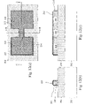
- FIG. 2( a ) is a top view of a programmable eFUSE structure 200
- FIG. 2( b ) is a cross-sectional view taken along B-B of FIG. 2( a )
- FIG. 2( c ) is a cross-sectional view taken along C-C of FIG. 2( a ).
- a substrate 202 e.g., silicon, silicon-on-insulator, etc.
- an insulating layer e.g., shallow trench isolation
- polysilicon material formed over the insulating layer 204 is patterned so as to form the heater electrodes 206 , as well as the thin wire structure 208 that electrically connects the heater electrodes 206 .
- a thin layer of oxide 210 covers the sidewalls of the electrodes 206 and wire structure 208 .
- the polysilicon material is provided with silicide metal contacts for ohmic contact with upper wiring levels.
- a silicide layer 212 is formed over polysilicon by deposition of a suitable refractory metal (e.g., cobalt, nickel, titanium, tantalum, tungsten, platinum, erbium, ytterbium, etc.) followed by a high-temperature anneal.
- a suitable refractory metal e.g., cobalt, nickel, titanium, tantalum, tungsten, platinum, erbium, ytterbium, etc.
- the portions of the metal layer in contact with silicon react with the silicon during the anneal to form a conductive silicide metal layer.
- a self-aligning process with respect to silicon it is also known in the art as a “salicide” process.
- a layer of PCM 214 is formed over the heater element in a generally perpendicular direction with respect to the orientation of the wire structure 208 , as best seen in FIG. 2( b ).
- An extended portion 215 of the PCM 214 extends along the insulating layer 204 adjacent the wire structure 208 so as to provide a contact point for the functional portion of the eFUSE device (i.e., a point at which the programmed state of the fuse may be sensed).
- the extended portion 215 provides a surface upon which conductive vias 216 may be subsequently defined once an interlevel dielectric (ILD) layer 218 (not shown in FIG. 2( a )) is formed over the structure. Additional vias 216 are also formed on the heater electrodes 206 in order to run heating current through the wire structure 208 . Sequential processing views illustrating the formation steps in further detail, as well as exemplary processing conditions, are presented hereinafter.
- FIG. 3 is a schematic diagram illustrating the operation of the programmable eFUSE structure 200 of FIG. 2 , in conjunction with an exemplary sensing circuit 300 , in accordance with an further embodiment of the invention.
- the heater circuit (defined by electrodes 206 and connecting wire structure 208 ) is connected between a power supply V pp and ground through a programming FET 302 , which has a control signal V_gate applied to the gate terminal thereof.
- the PCM layer 214 formed over the wire structure 208 has the extended portion 215 thereof connected (through vias 216 ) to an input node of a sense inverter 304 , as well as to ground through a reference resistor R 0 .
- the programming transistor 302 e.g., an NFET
- the programming transistor 302 is activated by a relatively high input voltage on V gate to deliver a high current, followed by a rapid shut off of the transistor 302 .
- heat is rapidly conducted away from the silicide material 212 and PCM layer 214 , through the polysilicon, resulting in a quench of the PCM 214 .
- the portion of the PCM layer 214 in proximity to the silicide heater (shown in different shading in FIG. 4 ) is converted to the amorphous, high resistance state.
- the voltage on the input of the inverter 304 will discharge to ground through R 0 , thereby driving the sense output high.
- the anneal or SET operation is implemented by turning on transistor 302 with a relatively low input voltage on V gate to deliver a lower current with respect to the RESET operation, and thereafter shutting off transistor 302 .
- the high resistance portion of the PCM layer 214 is annealed back to the low resistance, crystalline state shown in FIG. 3 , thereby restoring the electrical connection between the PCM terminal (extended portion 215 ) and the power supply V pp .
- the voltage of the inverter input node across R 0 goes high, and the sense output is driven back to a low value.
- FIGS. 5( a ) through 5 ( c ) illustrate various top and cross-sectional views of a non-volatile memory cell using an externally heated PCM, and which is formed at the gate-level of device processing, in accordance with a further embodiment of the invention.
- the memory cell 500 in FIGS. 5( a ) through 5 ( c ) includes a substantially similar heater and PCM layer configuration, with the addition of a programming transistor 502 in series with one of the heater electrodes 206 .
- the programming transistor 502 include a polysilicon gate conductor 504 formed over a gate insulating layer 506 , which is in turn formed over a non-insulated portion of the substrate 202 . Integration of the programming transistor is fairly straightforward with respect to CMOS processing, including doping of the source/drain regions 508 . It is noted that during silicidation, silicide contacts 212 are also formed over the silicon containing gate conductor 504 and source/drain regions 508 . Also illustrated in FIGS.
- 5( a ) through 5 ( c ) is a first wiring layer 510 that is used, for example, to connect the programming transistor to one of the heater electrodes 206 , as well as to connect the other heater electrode to the power source and connect the PCM layer 214 to the associated sense circuitry.
- the sense circuitry associated with the non-volatile memory cell 500 does not typically rely on the heater supply voltage to supply an input signal thereto.
- V pp is separate from the sensing voltage, Vs, which is used as the input to the sense circuitry (not shown in FIG. 6 ).
- Vs the sensing voltage
- Rv The amount of current flowing through the PCM resistor, Rv, is dependent on the state of the PCM (i.e., large when it is in the low resistance crystalline state, and very low when it is in the high resistance amorphous state).
- FIGS. 7( a ) through 7 ( c ) various embodiments of sensing circuitry for an array of PCM memory cells such as shown in FIG. 5 are depicted.
- the arrays are depicted as 2 ⁇ 2; however, it will be appreciated that the principles described herein are applicable to larger arrays.
- FIG. 7( a ) illustrates an exemplary sense array circuit 700 .
- each cell includes an additional sense transistor 704 configured to pass a lower current with respect to the programming transistor 702 .
- This configuration prevents current from circulating between the program lines (PA, PB, etc.) and the sense lines (SA, SB, etc.) through non-selected cells in a given column.
- an adjustable power supply 706 VpA, VpB, etc.
- a fixed power supply 708 VsA, VsB, etc.
- the power supplies may be located on the same circuit board as the sense array circuit 700 , or they may be located on a different component altogether. In the latter instance, the off-chip sources would be coupled to corresponding power source nodes on the chip containing the sense array circuit 700 .
- the PA switches are closed and the SA switches are opened.
- a programming (high) voltage is thus applied by the adjustable power supply 706 to the appropriate Vp line connected to the cell, and the gate line (e.g., Vg 1 , Vg 2 , etc.) corresponding to the cell to be programmed is pulsed.
- the magnitude and duration of the pulse is selected between one having a low magnitude and slow ramp down (e.g., low resistance for writing a logical 0) and one having a large magnitude and fast ramp down (e.g., high resistance for writing a logical 1).
- programming can be done for all 0's or all 1's on the same gate line at the same time.
- a cell in column A For example, the PA switches are opened and the SA switches are closed. A sensing (low) voltage, below the programming threshold, is then applied to the sense line VsA, and the gate line (e.g., Vg 1 , Vg 2 , etc.) corresponding to the cell to be sensed is pulsed. A parallel output of all cells attached to the selected gate line is coupled to the corresponding current sense output 710 , thus generating, for example, Sense_out_A in column A.
- the gate line e.g., Vg 1 , Vg 2 , etc.
- FIG. 7( b ) illustrates an alternative embodiment 720 of the sense array circuit of FIG. 7( a ), wherein the sense transistors 704 in each cell are instead replaced by a common transistor 712 for each row (gate line) in the peripheral circuitry.
- the operations for programming/sensing a single cell are the same as described in FIG. 7( a ). It will be noted that in the FIG. 7( b ) design, it may not be practical to simultaneously sense or program large numbers of cells in a selected row if the common transistor 712 has to be too large.
- FIG. 7( c ) illustrates still another embodiment of the sense array circuit 740 in which the sense current passed through Rv is converted to a voltage through a small reference resistor “r” (wherein r is on the order of about 1-100 ⁇ ).
- the value of the reference resistor is kept very small; otherwise, it would be shunted by up to N (where N is the number of rows, e.g., 512) resistors (Rv+Rh/2) between the sense and programming lines. Shunting leads to an undesired dependence of the sense output on the state of the memory rather than just the state of the selected cell.
- r ⁇ (Rv+Rh/2)/N, where Rv is the resistance value of the PCM in the crystalline state.
- the column sense amplifiers 710 are pulse voltage-amplifiers having a high gain of order N (e.g., on the order of about 1000); their design is facilitated by the low source resistance r. It will also be noted that a single adjustable power supply 706 (VpA, VpB, etc.) is provided per column. In this embodiment, significant current circulating between the program and sense lines in a given column in non-selected cells is prevented by the close proximity of the voltages of the programming and sense lines.
- the array of FIG. 7( c ) is programmed by application of a high voltage to the appropriate Vp line (A, B, etc.) connected to the cell, followed by pulsing the gate line for the cell.
- the magnitude and duration of the pulse is selected between one having a low magnitude and slow ramp down (e.g., low resistance for writing a logical 0) and one having a large magnitude and fast ramp down (e.g., high resistance for writing a logical 1).
- programming can be done for all 0's or all 1's on the same gate line at the same time.
- a low voltage (below the programming threshold) is applied to the corresponding Vp line (A, B, etc.) connected to the cell, followed by pulsing the gate line for the cell.
- a parallel output of all cells attached to the selected gate line is coupled to the corresponding current sense output 710 , thus generating, for example, Sense_out_A.
- certain key aspects of the operation of a PCM device include the quench time and the quench (RESET) power.
- the quench time must be short (e.g., on a nanosecond time scale), in order for the melted PCM material cool to the amorphous state rather than recrystallizing.
- the power required to melt the material is supplied through a programming transistor, and the length of this transistor scales in accordance with the programming current supplied thereby.
- the transistor width is a main factor in the area per stored memory bit. Thus, minimizing programming power is a key factor in minimizing the area per bit.
- FIGS. 9( a ) and 9 ( b ) the results of a 3D simulation of a gate-level PCM eFUSE 900 similar to the embodiment of FIG. 2 are illustrated.
- the cross-sectional view of FIG. 9( a ) generally corresponds to the view seen in FIG. 2( c ), while the cross-sectional view of FIG. 9( b ) generally corresponds to the view seen in FIG. 2( b ).
- the eFUSE device 900 measured 1.28 ⁇ 0.58 ⁇ 0.38 ⁇ m 3
- the cathode and anode in-plane dimensions are 0.3 ⁇ 0.3 ⁇ m 2
- the silicide strip (wire structure 208 ) connecting them is 0.40 ⁇ m long and 0.03 ⁇ m thick.
- the PCM 214 is 0.12 ⁇ m wide parallel to the silicide strip portion of the wire structure 208 , and 0.05 ⁇ m thick.
- a temperature dependent heating rate was applied to the silicide for 34 ns, followed by a zero heating rate for an additional 6 ns.
- the temperature increases at all locations of the device during the heating, causing the melting of all portions of the PCM 214 in contact with the silicide 212 .
- the heating rate drops to zero, the temperature correspondingly decreases at all locations, but in particular, the temperature in the PCM 214 drops very suddenly (to below the melting temperature) within about 1 ns. This is fast enough to quench the PCM and render it non-conducting.
- FIGS. 9( a ) and 9 ( b ) depict the temperature distribution just before quenching with an outer temperature contour 904 at about 255° C. and an inner temperature contour 902 at the PCM melting temperature, assumed to be 607° C. At this point, all of the PCM within the inner temperature contour 902 is melted.
- the average power input to the silicide during the heating phase is 2.4 mW.
- the peak temperature after 34 ns is about 847° C., which sufficiently low to preserve the integrity of the materials.
- Various other designs, dimensions, and heating rates were simulated as well, demonstrating the desired PCM melting temperatures with reasonably low applied power levels and low peak temperatures in the silicide material.
- the silicide material used in forming conductive contacts for FET devices at the substrate level is also used to form the electrodes and wire structure of the heater circuit.
- An exemplary process of record utilizes nickel mono-silicide (NiSi) doped with about 5% Pt as silicide metal.
- NiSi nickel mono-silicide
- other di-silicide materials such as CoSi 2 or TiSi 2 , for example, may need to be considered, depending on the required power/temperature rise during the quench/anneal cycles.
- CoSi 2 or TiSi 2 existing processes of record for silicide contact formation are also available for ease of integration of the PCM devices into CMOS processing. The relative advantages or disadvantages of three different silicides are illustrated in FIG. 10 .
- the melting temperature of NiSi is the lowest (less than 1000° C.), while that of TiSi 2 is the highest.
- the silicide stability at high temperatures affects the capability of maximizing the multishot (reprogrammablility) feature of the eFUSE/memory cell.
- multiple silicide phases having different resistivities may be formed.
- changing silicide resistivity may be problematic in terms of controlling and managing power inputs during the quench/anneal cycles.
- NiSi certain challenges include more complex phase formation (multiple metal rich phases), the possibility of forming higher resistivity NiSi 2 in BEOL anneals, and lower morphological stability.
- one advantage of NiSi is that it addresses the problem of voiding in narrow polysilicon lines, provided that measures are taken to prevent other silicide phases from forming. This may be achieved by an additional doping (e.g., Re, Rh or Hf, in addition to Pt).
- Rutherford Backscattering Spectroscopy (RBS) analysis of a GST-225/NiSi (5% Pt) interface indicates stable at least up to about 505° C.
- a thin native (about 25 ⁇ ) SiO 2 layer on the surface of the silicide acts as a (inter) diffusion barrier.
- a thin Ti layer at the interface to form GST-225/Ti/NiSi (5% Pt) stack, some interface reaction is taking place, since Ti is a very effective oxygen getter (by reducing the SiO 2 on the NiSi and/or diffusing into the GST).
- a barrier layer of nitride or oxide may be used.
- FIGS. 11 through 14 are top and cross-sectional views illustrating a more detailed, sequential description of an exemplary method of forming the eFUSE device of FIG. 2 .
- the structures in FIGS. 11( a ) through 11 ( c ) are formed in conformance with standard CMOS processing.
- the active areas are defined by forming the STI regions 204 on the substrate.
- the heating element comprising the anode, cathode (electrodes 206 ) and the heater link (wire structure 208 ) is formed during the polysilicon conductor formation process (material deposition, lithographic patterning and etching) and the subsequent nitride spacer formation process.
- FIGS. 12( a ) through 12 ( c ) illustrate the device as a result the salicidation process.
- the device is wet cleaned using 40:1 BHF (buffered hydrofluoric acid) for 45 seconds prior to the sputter deposition of about 8 nm of a NiPt alloy (95% Ni, 5% Pt) and 5 nm of TiN as a silicide metal material.
- a short time anneal of about 5 seconds is used to react the P+ polysilicon (120 nm) with the deposited NiPt (8 nm) to form about a 16 nm NiPt (95% Ni, 5% Pt) silicide layer 212 .
- the unreacted NiPt metal is removed by etching in aqua regia (a mixture of 5 parts concentrated (37%) hydrochloric acid, 1 part concentrated (70%) nitric acid, and 4 parts deionized water) for several minutes. A second, longer duration homogenization anneal completes the silicidation at about 500° C.
- FIGS. 13( a ) through 13 ( c ) an additional process for deposition and patterning of the PCM material 214 (e.g., GST) is shown.
- the device is shown after MOL (middle of the line) dielectric deposition 218 and contact (via 216 ) formation.
- MOL middle of the line
- contact formation is implemented through lithographic patterning and etching of dielectric layer 218 , followed by damascene metal (e.g., W) deposition and planarization. Subsequent processing is thereafter continued in accordance with standard logic processing techniques.
- damascene metal e.g., W
Landscapes
- Engineering & Computer Science (AREA)
- Chemical & Material Sciences (AREA)
- Crystallography & Structural Chemistry (AREA)
- Manufacturing & Machinery (AREA)
- Computer Hardware Design (AREA)
- Semiconductor Memories (AREA)
Abstract
Description
C V dT/dt=∇K∇T+H
Claims (5)
Priority Applications (3)
| Application Number | Priority Date | Filing Date | Title |
|---|---|---|---|
| US11/672,110 US7411818B1 (en) | 2007-02-07 | 2007-02-07 | Programmable fuse/non-volatile memory structures using externally heated phase change material |
| CN2008100020851A CN101241926B (en) | 2007-02-07 | 2008-01-16 | Programmable phase change material structure and its forming method |
| US12/127,909 US20080285335A1 (en) | 2007-02-07 | 2008-05-28 | Programmable fuse/non-volatile memory structures using externally heated phase change material |
Applications Claiming Priority (1)
| Application Number | Priority Date | Filing Date | Title |
|---|---|---|---|
| US11/672,110 US7411818B1 (en) | 2007-02-07 | 2007-02-07 | Programmable fuse/non-volatile memory structures using externally heated phase change material |
Related Child Applications (1)
| Application Number | Title | Priority Date | Filing Date |
|---|---|---|---|
| US12/127,909 Continuation US20080285335A1 (en) | 2007-02-07 | 2008-05-28 | Programmable fuse/non-volatile memory structures using externally heated phase change material |
Publications (2)
| Publication Number | Publication Date |
|---|---|
| US20080186760A1 US20080186760A1 (en) | 2008-08-07 |
| US7411818B1 true US7411818B1 (en) | 2008-08-12 |
Family
ID=39676006
Family Applications (2)
| Application Number | Title | Priority Date | Filing Date |
|---|---|---|---|
| US11/672,110 Active US7411818B1 (en) | 2007-02-07 | 2007-02-07 | Programmable fuse/non-volatile memory structures using externally heated phase change material |
| US12/127,909 Abandoned US20080285335A1 (en) | 2007-02-07 | 2008-05-28 | Programmable fuse/non-volatile memory structures using externally heated phase change material |
Family Applications After (1)
| Application Number | Title | Priority Date | Filing Date |
|---|---|---|---|
| US12/127,909 Abandoned US20080285335A1 (en) | 2007-02-07 | 2008-05-28 | Programmable fuse/non-volatile memory structures using externally heated phase change material |
Country Status (2)
| Country | Link |
|---|---|
| US (2) | US7411818B1 (en) |
| CN (1) | CN101241926B (en) |
Cited By (22)
| Publication number | Priority date | Publication date | Assignee | Title |
|---|---|---|---|---|
| US20070194294A1 (en) * | 2006-02-21 | 2007-08-23 | Samsung Electronics Co., Ltd. | Phase change memory devices and methods for fabricating the same |
| US20080210925A1 (en) * | 2006-03-30 | 2008-09-04 | International Business Machines Corporation | Three-terminal cascade switch for controlling static power consumption in integrated circuits |
| US20090045484A1 (en) * | 2007-08-16 | 2009-02-19 | International Business Machines Corporation | Methods and systems involving electrically reprogrammable fuses |
| US20090065761A1 (en) * | 2007-09-06 | 2009-03-12 | International Business Machine Corporation | Programmable fuse/non-volatile memory structures in beol regions using externally heated phase change material |
| US20100073997A1 (en) * | 2008-09-19 | 2010-03-25 | International Business Machines Corporation | Piezo-driven non-volatile memory cell with hysteretic resistance |
| US7855909B1 (en) * | 2007-04-10 | 2010-12-21 | Marvell International Ltd. | Calibrating page borders in a phase-change memory |
| US20100328984A1 (en) * | 2009-06-30 | 2010-12-30 | International Business Machines Corporation | Piezo-effect transistor device and applications |
| US20110075469A1 (en) * | 2009-03-25 | 2011-03-31 | Zhiqiang Wei | Resistance variable nonvolatile memory device |
| US7936582B1 (en) * | 2008-03-19 | 2011-05-03 | Xilinx, Inc. | E-fuse read circuit with dual comparators |
| US20110133603A1 (en) * | 2009-12-07 | 2011-06-09 | International Business Machines Corporation | Coupling piezoelectric material generated stresses to devices formed in integrated circuits |
| US20120049144A1 (en) * | 2010-08-31 | 2012-03-01 | International Business Machines Corporation | Post-Fabrication Self-Aligned Initialization of Integrated Devices |
| US8208294B2 (en) | 2009-01-23 | 2012-06-26 | Qimonda Ag | Resistive memory cell accessed using two bit lines |
| US8624217B2 (en) | 2010-06-25 | 2014-01-07 | International Business Machines Corporation | Planar phase-change memory cell with parallel electrical paths |
| US8644053B2 (en) * | 2011-11-15 | 2014-02-04 | Stmicroelectronics Pte Ltd. | Resistor thin film MTP memory |
| US8809861B2 (en) | 2010-12-29 | 2014-08-19 | Stmicroelectronics Pte Ltd. | Thin film metal-dielectric-metal transistor |
| US8927909B2 (en) | 2010-10-11 | 2015-01-06 | Stmicroelectronics, Inc. | Closed loop temperature controlled circuit to improve device stability |
| US9159413B2 (en) | 2010-12-29 | 2015-10-13 | Stmicroelectronics Pte Ltd. | Thermo programmable resistor based ROM |
| US9251884B2 (en) | 2014-03-24 | 2016-02-02 | International Business Machines Corporation | Non-volatile, piezoelectronic memory based on piezoresistive strain produced by piezoelectric remanence |
| US10964881B2 (en) | 2014-03-10 | 2021-03-30 | International Business Machines Corporation | Piezoelectronic device with novel force amplification |
| US11270768B2 (en) | 2020-03-04 | 2022-03-08 | International Business Machines Corporation | Failure prevention of chip power network |
| US11437102B1 (en) | 2021-03-05 | 2022-09-06 | International Business Machines Corporation | Memory erasure using proximity heaters |
| US11818886B2 (en) | 2021-09-29 | 2023-11-14 | International Business Machines Corporation | Low program voltage flash memory cells with embedded heater in the control gate |
Families Citing this family (16)
| Publication number | Priority date | Publication date | Assignee | Title |
|---|---|---|---|---|
| US8563355B2 (en) * | 2008-01-18 | 2013-10-22 | Freescale Semiconductor, Inc. | Method of making a phase change memory cell having a silicide heater in conjunction with a FinFET |
| US8043888B2 (en) | 2008-01-18 | 2011-10-25 | Freescale Semiconductor, Inc. | Phase change memory cell with heater and method therefor |
| US8062977B1 (en) | 2008-01-31 | 2011-11-22 | Novellus Systems, Inc. | Ternary tungsten-containing resistive thin films |
| KR101536562B1 (en) * | 2009-02-09 | 2015-07-14 | 삼성전자 주식회사 | Semiconductor integrated circuit device |
| US20110304404A1 (en) * | 2010-02-19 | 2011-12-15 | University Of Connecticut | Signal generators based on solid-liquid phase switching |
| CN102270497A (en) * | 2010-06-02 | 2011-12-07 | 王彬 | Memory utilizing shadow nonvolatile memory configured with redundancy storage |
| US8320172B2 (en) * | 2010-07-29 | 2012-11-27 | Micron Technology, Inc. | Write operation for phase change memory |
| KR102096614B1 (en) * | 2013-10-11 | 2020-04-03 | 삼성전자주식회사 | e-fuse structure of a semiconductor device |
| US10490374B2 (en) * | 2014-09-12 | 2019-11-26 | Northrop Grumman Systems Corporation | Phase-change material distributed switch systems |
| US10700270B2 (en) | 2016-06-21 | 2020-06-30 | Northrop Grumman Systems Corporation | PCM switch and method of making the same |
| US10580976B2 (en) | 2018-03-19 | 2020-03-03 | Sandisk Technologies Llc | Three-dimensional phase change memory device having a laterally constricted element and method of making the same |
| US10991879B2 (en) * | 2019-06-26 | 2021-04-27 | Western Digital Technologies, Inc. | Multi-level phase change memory cells and method of making the same |
| EP3876274A1 (en) * | 2020-03-05 | 2021-09-08 | Infineon Technologies AG | Integrated circuit, method for manufcaturing an integrated circuit, wafer and method for manufacturing a wafer |
| US11653578B2 (en) * | 2020-12-01 | 2023-05-16 | International Business Machines Corporation | Phase-change material-based XOR logic gates |
| US11546010B2 (en) | 2021-02-16 | 2023-01-03 | Northrop Grumman Systems Corporation | Hybrid high-speed and high-performance switch system |
| US20230070462A1 (en) * | 2021-09-09 | 2023-03-09 | International Business Machines Corporation | Wrap-around projection liner for ai device |
Citations (11)
| Publication number | Priority date | Publication date | Assignee | Title |
|---|---|---|---|---|
| US6448576B1 (en) | 2001-08-30 | 2002-09-10 | Bae Systems Information And Electronic Systems Integration, Inc. | Programmable chalcogenide fuse within a semiconductor device |
| US20050121789A1 (en) | 2003-12-04 | 2005-06-09 | Madurawe Raminda U. | Programmable structured arrays |
| US20050188230A1 (en) | 2004-02-20 | 2005-08-25 | International Business Machines Corporation | System and method of controlling power consumption in an electronic system |
| US6970034B1 (en) | 2003-07-07 | 2005-11-29 | Sun Microsystems, Inc. | Method and apparatus for reducing power consumption due to gate leakage during sleep mode |
| US20060278895A1 (en) | 2005-06-14 | 2006-12-14 | International Business Machines Corporation | Reprogrammable fuse structure and method |
| US20060279978A1 (en) | 2005-06-13 | 2006-12-14 | International Business Machines Corporation | Method and structure for high performance phase change memory |
| US7208751B2 (en) | 2002-09-13 | 2007-04-24 | Renesas Technology Corp. | Non-volatile semiconductor memory device allowing shrinking of memory cell |
| US20070295948A1 (en) | 2006-06-07 | 2007-12-27 | International Business Machines Corporation | Nonvolatile memory cell with concentric phase change material formed around a pillar arrangement |
| US20080017842A1 (en) | 2006-07-20 | 2008-01-24 | Thomas Happ | Phase change memory cell including nanocomposite insulator |
| US7324365B2 (en) * | 2006-03-02 | 2008-01-29 | Infineon Technologies Ag | Phase change memory fabricated using self-aligned processing |
| US20080048169A1 (en) * | 2006-08-25 | 2008-02-28 | International Business Machines Corporation | Heat-shielded low power pcm-based reprogrammable efuse device |
Family Cites Families (7)
| Publication number | Priority date | Publication date | Assignee | Title |
|---|---|---|---|---|
| EP1228016B1 (en) * | 1999-11-04 | 2005-03-30 | Pretoria Portland Cement Company Limited | Kiln plant control system |
| US20050158950A1 (en) * | 2002-12-19 | 2005-07-21 | Matrix Semiconductor, Inc. | Non-volatile memory cell comprising a dielectric layer and a phase change material in series |
| KR100491978B1 (en) * | 2003-04-12 | 2005-05-27 | 한국전자통신연구원 | Phase change memory element capable of low power operation and method for fabricating the same |
| JP2005032855A (en) * | 2003-07-09 | 2005-02-03 | Matsushita Electric Ind Co Ltd | Semiconductor storage device and its fabricating process |
| US7391642B2 (en) * | 2005-01-25 | 2008-06-24 | Intel Corporation | Multilevel programming of phase change memory cells |
| US7494849B2 (en) * | 2005-11-03 | 2009-02-24 | Cswitch Inc. | Methods for fabricating multi-terminal phase change devices |
| US8183551B2 (en) * | 2005-11-03 | 2012-05-22 | Agale Logic, Inc. | Multi-terminal phase change devices |
-
2007
- 2007-02-07 US US11/672,110 patent/US7411818B1/en active Active
-
2008
- 2008-01-16 CN CN2008100020851A patent/CN101241926B/en not_active Expired - Fee Related
- 2008-05-28 US US12/127,909 patent/US20080285335A1/en not_active Abandoned
Patent Citations (12)
| Publication number | Priority date | Publication date | Assignee | Title |
|---|---|---|---|---|
| US6448576B1 (en) | 2001-08-30 | 2002-09-10 | Bae Systems Information And Electronic Systems Integration, Inc. | Programmable chalcogenide fuse within a semiconductor device |
| US7208751B2 (en) | 2002-09-13 | 2007-04-24 | Renesas Technology Corp. | Non-volatile semiconductor memory device allowing shrinking of memory cell |
| US6970034B1 (en) | 2003-07-07 | 2005-11-29 | Sun Microsystems, Inc. | Method and apparatus for reducing power consumption due to gate leakage during sleep mode |
| US20050121789A1 (en) | 2003-12-04 | 2005-06-09 | Madurawe Raminda U. | Programmable structured arrays |
| US20050188230A1 (en) | 2004-02-20 | 2005-08-25 | International Business Machines Corporation | System and method of controlling power consumption in an electronic system |
| US20060279978A1 (en) | 2005-06-13 | 2006-12-14 | International Business Machines Corporation | Method and structure for high performance phase change memory |
| US7221579B2 (en) | 2005-06-13 | 2007-05-22 | International Business Machines Corporation | Method and structure for high performance phase change memory |
| US20060278895A1 (en) | 2005-06-14 | 2006-12-14 | International Business Machines Corporation | Reprogrammable fuse structure and method |
| US7324365B2 (en) * | 2006-03-02 | 2008-01-29 | Infineon Technologies Ag | Phase change memory fabricated using self-aligned processing |
| US20070295948A1 (en) | 2006-06-07 | 2007-12-27 | International Business Machines Corporation | Nonvolatile memory cell with concentric phase change material formed around a pillar arrangement |
| US20080017842A1 (en) | 2006-07-20 | 2008-01-24 | Thomas Happ | Phase change memory cell including nanocomposite insulator |
| US20080048169A1 (en) * | 2006-08-25 | 2008-02-28 | International Business Machines Corporation | Heat-shielded low power pcm-based reprogrammable efuse device |
Non-Patent Citations (17)
| Title |
|---|
| "Exploring Potential Benefits of 3D FPGA Integration" 1-6 pages. |
| C.J. Glassbrenner et al.; "Thermal Conductivity of Silicon and Germanium from 3° K to the Melting Point*;" Physical Review vol. 134, No. 4A; May 18, 1964; pp. A1058-A1069. |
| file://C:\DOCUME~1\ADMINI~1\LOCALS~\Temp\V9K43UPW.htm, Jul. 20, 2005, "What Are CPLDs and FPGAs", 1-3 pages. |
| J. Appl. Phys. 82 (9), Nov. 1, 1997, "Experimental and theoretical investigations of laser-induced crystallization and amorphization in phase-change optical recording media", Chubing Peng, Lu Cheng, and M. Mansurpur, pp. 4183-4191. |
| J. Maimon et al; "Chalcogenide-Based Non-Volatile Memory Technology;" IEEE; 2001 pp. 5-2289-5-2294. |
| Journal of Applied Physics 97, 083520 (2005), "Phase-change recording materials with a growth-dominated crystallization mechanism: A materials overview", L. van Pieterson, M. H. R. Lankhorst, M. van Schijndel, A. E. T. Kuiper, and J. H. J. Roosen, 1-7 pages. |
| Journal of Applied Physics, vol. 86, No. 4, Aug. 15, 1999, "Modeling of laser pulsed heating and quenching in optical data storage media", C. A. Volkert and M. Wuttig, pp. 1808-1816. |
| Jpn. J. Appl. Phys. vol. 40 (2001) Part 2, No. 6B, Jun. 15, 2001, "Temperature Dependence of TaSiN Thin Film Resistivity from Room Temperature to 900°C", Munenori Oizumi, Katsuhiro Aoki, and Yukio Fukuda, pp. L603-L605. |
| Jpn. J. Appl. Phys. vol. 42 (2003), Part 1, No. 2B, Feb. 2003, "Determination of the Crystallisation Kinetics of Fast-Growth Phase-Change Materials for Mark-Formation Prediction", Erwin R. Meinders and Martijn H. R. Lankhorst, pp. 809-812. |
| Physical Review Letters, vol. 64, No. 11, Mar. 12, 1990, "Asymmetric Crystallization and Melting Kinetitcs in Sodium: A Molecular-Dynamic Study", C. J. Tymczak and John R. Ray, pp. 1278-1281. |
| S. Lai et al; "OUM-A 180 nm Nonvaltile Memory Cell Element Technology for Stand Alone and Embedded Applications;" IEEE, 2001, pp. 36.5.1-36.5.4. |
| S. Tyson et al.; "Nonvolatile, High Density, High Performance Phase-Change Memory;" IEEE 2000; pp. 385-390. |
| Science, vol. 267, Mar. 31, 1995, "Formation of Glasses from Liquids and Biopolymers", C. A. Angell, pp. 1924-1934. |
| U.S. Appl. No. 11/833,321, filed Aug. 3, 2007. |
| U.S. Appl. No. 11/833,354, filed Aug. 3, 2007. |
| U.S. Appl. No. 11/958,298, filed Dec. 17, 2007. |
| Young-Tae Kim et al.; "Study on Cell Characteristics of PRAM Using the Phase-Change Simulation;" IEEE 2003; pp. 211-214. |
Cited By (49)
| Publication number | Priority date | Publication date | Assignee | Title |
|---|---|---|---|---|
| US20070194294A1 (en) * | 2006-02-21 | 2007-08-23 | Samsung Electronics Co., Ltd. | Phase change memory devices and methods for fabricating the same |
| US7667221B2 (en) * | 2006-02-21 | 2010-02-23 | Samsung Electronics Co., Ltd. | Phase change memory devices and methods for fabricating the same |
| US20080210925A1 (en) * | 2006-03-30 | 2008-09-04 | International Business Machines Corporation | Three-terminal cascade switch for controlling static power consumption in integrated circuits |
| US8586957B2 (en) | 2006-03-30 | 2013-11-19 | International Business Machines Corporation | Three-terminal cascade switch for controlling static power consumption in integrated circuits |
| US8466444B2 (en) | 2006-03-30 | 2013-06-18 | International Business Machines Corporation | Three-terminal cascade switch for controlling static power consumption in integrated circuits |
| US8143609B2 (en) | 2006-03-30 | 2012-03-27 | International Business Machines Corporation | Three-terminal cascade switch for controlling static power consumption in integrated circuits |
| US20090315010A1 (en) * | 2006-03-30 | 2009-12-24 | International Business Machines Corporation | Three-terminal cascade switch for controlling static power consumption in integrated circuits |
| US20090321710A1 (en) * | 2006-03-30 | 2009-12-31 | International Business Machines Corporation | Three-terminal cascade switch for controlling static power consumption in integrated circuits |
| US7652279B2 (en) | 2006-03-30 | 2010-01-26 | International Business Machines Corporation | Three-terminal cascade switch for controlling static power consumption in integrated circuits |
| US7855909B1 (en) * | 2007-04-10 | 2010-12-21 | Marvell International Ltd. | Calibrating page borders in a phase-change memory |
| US20090045484A1 (en) * | 2007-08-16 | 2009-02-19 | International Business Machines Corporation | Methods and systems involving electrically reprogrammable fuses |
| US20100118636A1 (en) * | 2007-08-16 | 2010-05-13 | International Business Machines Corporation | Methods and Systems Involving Electrically Reprogrammable Fuses |
| US8716071B2 (en) | 2007-08-16 | 2014-05-06 | International Business Machines Corporation | Methods and systems involving electrically reprogrammable fuses |
| US8866257B2 (en) | 2007-08-16 | 2014-10-21 | International Business Machines Corporation | System involving electrically reprogrammable fuses |
| US8535991B2 (en) | 2007-08-16 | 2013-09-17 | International Business Machines Corporation | Methods and systems involving electrically reprogrammable fuses |
| US20090065761A1 (en) * | 2007-09-06 | 2009-03-12 | International Business Machine Corporation | Programmable fuse/non-volatile memory structures in beol regions using externally heated phase change material |
| US7633079B2 (en) | 2007-09-06 | 2009-12-15 | International Business Machines Corporation | Programmable fuse/non-volatile memory structures in BEOL regions using externally heated phase change material |
| US7936582B1 (en) * | 2008-03-19 | 2011-05-03 | Xilinx, Inc. | E-fuse read circuit with dual comparators |
| US7848135B2 (en) | 2008-09-19 | 2010-12-07 | International Business Machines Corporation | Piezo-driven non-volatile memory cell with hysteretic resistance |
| US20100073997A1 (en) * | 2008-09-19 | 2010-03-25 | International Business Machines Corporation | Piezo-driven non-volatile memory cell with hysteretic resistance |
| US8208294B2 (en) | 2009-01-23 | 2012-06-26 | Qimonda Ag | Resistive memory cell accessed using two bit lines |
| US20110075469A1 (en) * | 2009-03-25 | 2011-03-31 | Zhiqiang Wei | Resistance variable nonvolatile memory device |
| US8320159B2 (en) * | 2009-03-25 | 2012-11-27 | Panasonic Corporation | Resistance variable nonvolatile memory device |
| US8159854B2 (en) | 2009-06-30 | 2012-04-17 | International Business Machines Corporation | Piezo-effect transistor device and applications |
| US20100328984A1 (en) * | 2009-06-30 | 2010-12-30 | International Business Machines Corporation | Piezo-effect transistor device and applications |
| US8405279B2 (en) | 2009-12-07 | 2013-03-26 | International Business Machines Corporation | Coupling piezoelectric material generated stresses to devices formed in integrated circuits |
| US8247947B2 (en) | 2009-12-07 | 2012-08-21 | International Business Machines Corporation | Coupling piezoelectric material generated stresses to devices formed in integrated circuits |
| US20110133603A1 (en) * | 2009-12-07 | 2011-06-09 | International Business Machines Corporation | Coupling piezoelectric material generated stresses to devices formed in integrated circuits |
| US8624217B2 (en) | 2010-06-25 | 2014-01-07 | International Business Machines Corporation | Planar phase-change memory cell with parallel electrical paths |
| US8861266B2 (en) | 2010-06-25 | 2014-10-14 | International Business Machines Corporation | Planar phase-change memory cell with parallel electrical paths |
| US8685785B2 (en) | 2010-06-25 | 2014-04-01 | International Business Machines Corporation | Planar phase-change memory cell with parallel electrical paths |
| US9196829B2 (en) | 2010-08-31 | 2015-11-24 | Globalfoundries Inc. | Post-fabrication self-aligned initialization of integrated devices |
| US20120049144A1 (en) * | 2010-08-31 | 2012-03-01 | International Business Machines Corporation | Post-Fabrication Self-Aligned Initialization of Integrated Devices |
| US8575008B2 (en) * | 2010-08-31 | 2013-11-05 | International Business Machines Corporation | Post-fabrication self-aligned initialization of integrated devices |
| US11140750B2 (en) | 2010-10-11 | 2021-10-05 | Stmicroelectronics, Inc. | Closed loop temperature controlled circuit to improve device stability |
| US10206247B2 (en) | 2010-10-11 | 2019-02-12 | Stmicroelectronics, Inc. | Closed loop temperature controlled circuit to improve device stability |
| US8927909B2 (en) | 2010-10-11 | 2015-01-06 | Stmicroelectronics, Inc. | Closed loop temperature controlled circuit to improve device stability |
| US11856657B2 (en) | 2010-10-11 | 2023-12-26 | Stmicroelectronics Asia Pacific Pte Ltd | Closed loop temperature controlled circuit to improve device stability |
| US9165853B2 (en) | 2010-10-11 | 2015-10-20 | Stmicroelectronics Asia Pacific Pte. Ltd. | Closed loop temperature controlled circuit to improve device stability |
| US8809861B2 (en) | 2010-12-29 | 2014-08-19 | Stmicroelectronics Pte Ltd. | Thin film metal-dielectric-metal transistor |
| US9159413B2 (en) | 2010-12-29 | 2015-10-13 | Stmicroelectronics Pte Ltd. | Thermo programmable resistor based ROM |
| US8644053B2 (en) * | 2011-11-15 | 2014-02-04 | Stmicroelectronics Pte Ltd. | Resistor thin film MTP memory |
| US8885390B2 (en) | 2011-11-15 | 2014-11-11 | Stmicroelectronics Pte Ltd | Resistor thin film MTP memory |
| US10964881B2 (en) | 2014-03-10 | 2021-03-30 | International Business Machines Corporation | Piezoelectronic device with novel force amplification |
| US9251884B2 (en) | 2014-03-24 | 2016-02-02 | International Business Machines Corporation | Non-volatile, piezoelectronic memory based on piezoresistive strain produced by piezoelectric remanence |
| US9679645B2 (en) | 2014-03-24 | 2017-06-13 | International Business Machines Corporation | Non-volatile, piezoelectronic memory based on piezoresistive strain produced by piezoelectric remanence |
| US11270768B2 (en) | 2020-03-04 | 2022-03-08 | International Business Machines Corporation | Failure prevention of chip power network |
| US11437102B1 (en) | 2021-03-05 | 2022-09-06 | International Business Machines Corporation | Memory erasure using proximity heaters |
| US11818886B2 (en) | 2021-09-29 | 2023-11-14 | International Business Machines Corporation | Low program voltage flash memory cells with embedded heater in the control gate |
Also Published As
| Publication number | Publication date |
|---|---|
| US20080285335A1 (en) | 2008-11-20 |
| US20080186760A1 (en) | 2008-08-07 |
| CN101241926B (en) | 2010-06-16 |
| CN101241926A (en) | 2008-08-13 |
Similar Documents
| Publication | Publication Date | Title |
|---|---|---|
| US7411818B1 (en) | Programmable fuse/non-volatile memory structures using externally heated phase change material | |
| US7633079B2 (en) | Programmable fuse/non-volatile memory structures in BEOL regions using externally heated phase change material | |
| US7684235B2 (en) | Phase change memory | |
| US8493772B2 (en) | Phase change memory structures and methods | |
| US7381611B2 (en) | Multilayered phase change memory | |
| EP1326254B1 (en) | Architecture of a phase-change nonvolatile memory array | |
| US7709822B2 (en) | Phase change memory and manufacturing method thereof | |
| US9747975B2 (en) | Multi-level phase change memory | |
| EP1878064B1 (en) | Method and structure for peltier-controlled phase change memory | |
| US8030734B2 (en) | Forming phase change memories with a breakdown layer sandwiched by phase change memory material | |
| US20120294076A1 (en) | Forming Sublithographic Heaters for Phase Change Memories | |
| US20160211017A1 (en) | Heating phase change material | |
| US7655938B2 (en) | Phase change memory with U-shaped chalcogenide cell | |
| US20120080657A1 (en) | Low operational current phase change memory structures | |
| JPWO2010140210A1 (en) | Semiconductor memory device and manufacturing method thereof | |
| US20060255328A1 (en) | Using conductive oxidation for phase change memory electrodes | |
| CN116490058A (en) | Phase change memory cell, memory device, and corresponding methods | |
| US20110079763A1 (en) | Phase change devices |
Legal Events
| Date | Code | Title | Description |
|---|---|---|---|
| AS | Assignment |
Owner name: INTERNATIONAL BUSINESS MACHINES CORPORATION, NEW Y Free format text: ASSIGNMENT OF ASSIGNORS INTEREST;ASSIGNORS:ELMEGREEN, BRUCE G.;IYER, SUBRAMANIAN S.;KIM, DEOK-KEE;AND OTHERS;REEL/FRAME:018863/0099;SIGNING DATES FROM 20070130 TO 20070202 |
|
| FEPP | Fee payment procedure |
Free format text: PAYOR NUMBER ASSIGNED (ORIGINAL EVENT CODE: ASPN); ENTITY STATUS OF PATENT OWNER: LARGE ENTITY |
|
| STCF | Information on status: patent grant |
Free format text: PATENTED CASE |
|
| REMI | Maintenance fee reminder mailed | ||
| FPAY | Fee payment |
Year of fee payment: 4 |
|
| SULP | Surcharge for late payment | ||
| AS | Assignment |
Owner name: GLOBALFOUNDRIES U.S. 2 LLC, NEW YORK Free format text: ASSIGNMENT OF ASSIGNORS INTEREST;ASSIGNOR:INTERNATIONAL BUSINESS MACHINES CORPORATION;REEL/FRAME:036550/0001 Effective date: 20150629 |
|
| AS | Assignment |
Owner name: GLOBALFOUNDRIES INC., CAYMAN ISLANDS Free format text: ASSIGNMENT OF ASSIGNORS INTEREST;ASSIGNORS:GLOBALFOUNDRIES U.S. 2 LLC;GLOBALFOUNDRIES U.S. INC.;REEL/FRAME:036779/0001 Effective date: 20150910 |
|
| FPAY | Fee payment |
Year of fee payment: 8 |
|
| AS | Assignment |
Owner name: WILMINGTON TRUST, NATIONAL ASSOCIATION, DELAWARE Free format text: SECURITY AGREEMENT;ASSIGNOR:GLOBALFOUNDRIES INC.;REEL/FRAME:049490/0001 Effective date: 20181127 |
|
| MAFP | Maintenance fee payment |
Free format text: PAYMENT OF MAINTENANCE FEE, 12TH YEAR, LARGE ENTITY (ORIGINAL EVENT CODE: M1553); ENTITY STATUS OF PATENT OWNER: LARGE ENTITY Year of fee payment: 12 |
|
| AS | Assignment |
Owner name: GLOBALFOUNDRIES U.S. INC., CALIFORNIA Free format text: ASSIGNMENT OF ASSIGNORS INTEREST;ASSIGNOR:GLOBALFOUNDRIES INC.;REEL/FRAME:054633/0001 Effective date: 20201022 |
|
| AS | Assignment |
Owner name: GLOBALFOUNDRIES INC., CAYMAN ISLANDS Free format text: RELEASE BY SECURED PARTY;ASSIGNOR:WILMINGTON TRUST, NATIONAL ASSOCIATION;REEL/FRAME:054636/0001 Effective date: 20201117 |
|
| AS | Assignment |
Owner name: GLOBALFOUNDRIES U.S. INC., NEW YORK Free format text: RELEASE BY SECURED PARTY;ASSIGNOR:WILMINGTON TRUST, NATIONAL ASSOCIATION;REEL/FRAME:056987/0001 Effective date: 20201117 |