US7383033B2 - Differential and quadrature harmonic VCO and methods therefor - Google Patents
Differential and quadrature harmonic VCO and methods therefor Download PDFInfo
- Publication number
- US7383033B2 US7383033B2 US11/056,522 US5652205A US7383033B2 US 7383033 B2 US7383033 B2 US 7383033B2 US 5652205 A US5652205 A US 5652205A US 7383033 B2 US7383033 B2 US 7383033B2
- Authority
- US
- United States
- Prior art keywords
- signal
- transistor
- signals
- harmonic
- drain
- Prior art date
- Legal status (The legal status is an assumption and is not a legal conclusion. Google has not performed a legal analysis and makes no representation as to the accuracy of the status listed.)
- Expired - Fee Related, expires
Links
- 238000000034 method Methods 0.000 title claims abstract description 28
- 230000010355 oscillation Effects 0.000 claims abstract description 30
- 239000003990 capacitor Substances 0.000 claims description 57
- 238000001514 detection method Methods 0.000 claims description 26
- 238000006243 chemical reaction Methods 0.000 claims description 21
- 230000008859 change Effects 0.000 claims description 6
- 239000000872 buffer Substances 0.000 claims description 5
- 238000010586 diagram Methods 0.000 description 11
- 238000001228 spectrum Methods 0.000 description 10
- 238000010168 coupling process Methods 0.000 description 8
- 230000008878 coupling Effects 0.000 description 7
- 238000005859 coupling reaction Methods 0.000 description 7
- 230000003111 delayed effect Effects 0.000 description 7
- 230000008901 benefit Effects 0.000 description 6
- 238000004519 manufacturing process Methods 0.000 description 4
- 239000000470 constituent Substances 0.000 description 3
- 230000003321 amplification Effects 0.000 description 2
- 238000004891 communication Methods 0.000 description 2
- 230000003247 decreasing effect Effects 0.000 description 2
- 238000013461 design Methods 0.000 description 2
- 238000005516 engineering process Methods 0.000 description 2
- 238000003199 nucleic acid amplification method Methods 0.000 description 2
- 230000008569 process Effects 0.000 description 2
- 230000007704 transition Effects 0.000 description 2
- 238000004458 analytical method Methods 0.000 description 1
- 238000006880 cross-coupling reaction Methods 0.000 description 1
- 230000007547 defect Effects 0.000 description 1
- 230000001419 dependent effect Effects 0.000 description 1
- 230000009977 dual effect Effects 0.000 description 1
- 230000000694 effects Effects 0.000 description 1
- 238000002347 injection Methods 0.000 description 1
- 239000007924 injection Substances 0.000 description 1
- 238000005259 measurement Methods 0.000 description 1
- 238000012986 modification Methods 0.000 description 1
- 230000004048 modification Effects 0.000 description 1
- 230000009467 reduction Effects 0.000 description 1
- 238000004088 simulation Methods 0.000 description 1
- 230000003595 spectral effect Effects 0.000 description 1
- 230000006641 stabilisation Effects 0.000 description 1
- 238000011105 stabilization Methods 0.000 description 1
Images


Classifications
-
- E—FIXED CONSTRUCTIONS
- E05—LOCKS; KEYS; WINDOW OR DOOR FITTINGS; SAFES
- E05B—LOCKS; ACCESSORIES THEREFOR; HANDCUFFS
- E05B47/00—Operating or controlling locks or other fastening devices by electric or magnetic means
- E05B47/02—Movement of the bolt by electromagnetic means; Adaptation of locks, latches, or parts thereof, for movement of the bolt by electromagnetic means
- E05B47/026—Movement of the bolt by electromagnetic means; Adaptation of locks, latches, or parts thereof, for movement of the bolt by electromagnetic means the bolt moving rectilinearly
-
- H—ELECTRICITY
- H03—ELECTRONIC CIRCUITRY
- H03L—AUTOMATIC CONTROL, STARTING, SYNCHRONISATION OR STABILISATION OF GENERATORS OF ELECTRONIC OSCILLATIONS OR PULSES
- H03L7/00—Automatic control of frequency or phase; Synchronisation
- H03L7/06—Automatic control of frequency or phase; Synchronisation using a reference signal applied to a frequency- or phase-locked loop
- H03L7/08—Details of the phase-locked loop
- H03L7/099—Details of the phase-locked loop concerning mainly the controlled oscillator of the loop
- H03L7/0995—Details of the phase-locked loop concerning mainly the controlled oscillator of the loop the oscillator comprising a ring oscillator
-
- H—ELECTRICITY
- H03—ELECTRONIC CIRCUITRY
- H03B—GENERATION OF OSCILLATIONS, DIRECTLY OR BY FREQUENCY-CHANGING, BY CIRCUITS EMPLOYING ACTIVE ELEMENTS WHICH OPERATE IN A NON-SWITCHING MANNER; GENERATION OF NOISE BY SUCH CIRCUITS
- H03B27/00—Generation of oscillations providing a plurality of outputs of the same frequency but differing in phase, other than merely two anti-phase outputs
-
- E—FIXED CONSTRUCTIONS
- E05—LOCKS; KEYS; WINDOW OR DOOR FITTINGS; SAFES
- E05B—LOCKS; ACCESSORIES THEREFOR; HANDCUFFS
- E05B49/00—Electric permutation locks; Circuits therefor ; Mechanical aspects of electronic locks; Mechanical keys therefor
Definitions
- the present invention relates in general to a voltage controlled oscillator (hereinafter, referred to as a ‘VCO’), and more particularly, to a VCO generating multi-phase, multi-harmonic output signals.
- VCO voltage controlled oscillator
- a voltage controlled oscillator is an oscillator whose frequency is adjusted by controlling an applied voltage and changed capacitance of a variable capacitor.
- VCOs are essential components in the architecture of all telecommunication systems.
- the VCO in modern data communication systems is employed as part of a phase locked loop (hereinafter, referred to as a ‘PLL’) that generates local oscillator (hereinafter, referred to as an ‘LO’) frequencies for an up and down conversion of a radio signal from/to a baseband of a transmitter and receiver.
- PLL phase locked loop
- LO local oscillator
- a transmitter-receiver chip can include a certain number of VCO circuits for generating LO signals. To cope with spectral purity and phase noise of communication systems, each VCO is stabilized with the PLL.
- an input signal should be converted to a quadrature baseband signal at the last down-conversion operation.
- a quadrature phase LO signal also called as a phase (I) and quadrature (Q) signal, or an IQ signal
- the IQ signal is generated by applying a poly-phase filter to outputs of a differential oscillator, or applying a divide-by-four circuit to a token ring structure, or employing various kinds of means such as coupled oscillators for example.
- FIG. 1 illustrates a multiphase output oscillator using a logic inverter gate.
- a plurality of ring oscillators are serially coupled in a loop. None of the oscillators oscillates freely because each oscillator adjusts its successor all the way around the loop.
- a phase transition between two points in the loop is expressed as an integer fraction of 360 degrees, and is dependent on the number of oscillators. In the case of an integer multiple of four oscillators, the maximum phase transition is 90 degrees.
- a radio frequency in the multiphase output oscillator can be separated to a different phase, first and second harmonics are inseparable. Therefore, the disclosure can only be used as a quadrature generator, not as a harmonic generator. Another defect of the disclosure is that because the circuits are organized in a ring oscillator building block, without an additional circuit, sufficient RF outputs and satisfactory noise performance can not be obtained.
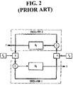
- FIG. 2 illustrates two fixed-frequency oscillators coupled in a ring topology.
- U.S. Pat. No. 6,188,292 discloses two interconnected oscillators where frequency variation is achieved by varying the coupling between the two oscillators. The coupling is varied by using a variable current or voltage source.
- this type of circuit can only be used as a quadrature generator, and is not appropriate for a harmonic generator.
- FIG. 3A illustrates a related art wide-band or multi-band voltage controlled oscillator.
- U.S. Pat. No. 6,417,740 disclosed this type of the VCO, in which a pair of LC oscillator circuits are cross-coupled through a transconductance control circuit.
- the tuning range is from 900 MHz to 1.3 GHz, and from 1.3 GHz to 2.4 GHz.
- the quadrature output voltage is ⁇ 10 dB, which corresponds to ⁇ 18 dBm at the impedance of the load 50 ohm.
- This type of circuit may be effectively used with a quadrature oscillator for a wide-band receiver system, but is not appropriate for the harmonic generator.
- FIG. 3B illustrates an embodiment of coupling for an LC-based VCO.
- U.S. Pat. No. 6,492,877 disclosed this type of coupling, in which two LC VCO signals are coupled through couplers or buffers and coupling loops, and the two-stage coupling loop system provides in-phase and quadrature signals in two stages.
- neither simulation nor measurement data is given, and there is no way to find out signal magnitude and a maximum system frequency (speed).
- a detailed schematic circuit diagram is not provided, it would be sufficient to note that the buffers in the disclosure reduce the load capacity of each VCO, and presumably improve the “performance” of the oscillator (this is not mentioned).
- the disclosed coupling method is effective for generating quadrature phase signals, but cannot generate differential phase signals.
- an aspect of the present invention to provide a voltage controlled oscillator, and method therefore, generating a quadrature and differential phase output signal at a first harmonic and a differential phase output signal at a second harmonic.
- Another aspect of the present invention is to provide a voltage controlled oscillator with an improved RF voltage, so that a second harmonic signal can be used without much amplification.
- a differential and quadrature harmonic voltage controlled oscillator including: a first oscillation unit for generating a first and a third signal; a first combining unit for combining the first and the third signal; a second oscillation unit for generating a second and a fourth signal; and a second combining unit for combining the second and the fourth signal, wherein the phase of the second signal is determined through a phase-invert and delay using the first signal; the phase of the third signal is determined through a phase-invert and delay using the second signal; the phase of the fourth signal is determined through a phase-invert and delay using the third signal; and the phase of the first signal is determined through a phase-invert and delay using the fourth signal.
- VCO differential and quadrature harmonic voltage controlled oscillator
- the VCO may further include: a first detection unit for detecting a first harmonic of the first, the second, the third, and the fourth signal, respectively; and a second detection unit for detecting a second harmonic of the first and the second combining unit, respectively.
- the first harmonics of the first and third signals may be differential signals
- the first harmonics of the second and fourth signals may be differential signals
- the first harmonics of the first and second signals may be quadrature signals.
- the second harmonic signals detected by the first and second combining units may also be differential signals.
- the first and the second oscillator may respectively include a tank circuit composed of at least one inductor and at least two variable capacitors.
- the first combining unit may further include a node where the first and third signals are combined, and a resistance connected to ground; and the second combining unit may include a node where the second and fourth signals are combined, and a resistance connected to ground.
- the frequency of the first, the second, the third, and the fourth signal may vary, according to the change in tuning voltage.
- the first oscillation unit may include: a first transistor having a source connected to ground; a second transistor having a drain connected to a gate of the first transistor, a gate connected to a drain of the first transistor, and a source commonly connected to the source of the first transistor and to ground; a fifth transistor having a drain connected to the drain of the first transistor; and a sixth transistor having a drain connected to the drain of the second transistor; and wherein the second oscillation unit may include: a third transistor having a source connected to ground; a fourth transistor having a drain connected to a gate of the third transistor, a gate connected to a drain of the third transistor, and a source commonly connected to the source of the third transistor and to ground; a seventh transistor having a drain connected to the drain of the third transistor; and an eighth transistor having a drain connected to a drain of the fourth transistor, wherein a gate of the seventh transistor is connected to the drain of the first transistor, the drain of the third transistor is connected to the gate of the sixth transistor, a gate of the eighth transistor is connected to
- the first through eighth transistors may be NMOS transistors.
- the first combining unit may include a first resistance, having one end of the first resistance commonly connected to the source of the fifth transistor and the source of the sixth transistor and the other end connected to ground; and the second combining unit may include a second resistance, having one end of the second resistance commonly connected to the source of the seventh transistor and the source of the eighth transistor and the other end connected to ground.
- the first oscillation unit may include: a first inductor, having one end connected to the drain of the first transistor and the other end connected to the drain of the second transistor; a first voltage; a first capacitor, having one end connected to one end of the first inductor and the other end connected to the first voltage; a second capacitor, having one end commonly connected to the other end of the first capacitor and the first voltage, and the other end connected to the other end of the first inductor; a second voltage; a ninth transistor, having a drain connected to one end of the first capacitor, and a source connected to the second voltage; and a tenth transistor, having a source connected to the second voltage, and a drain connected to the other end of the second capacitor, and a gate connected to a drain of the ninth transistor; and wherein the second oscillation unit may include: a second inductor, having one end connected to the drain of the third transistor and the other end connected to the drain of the fourth transistor; a third voltage; a third capacitor, having one end connected to one end of the second induct
- the first to eighth transistors may be NMOS transistors, and the ninth to twelfth transistors may be PMOS transistors.
- the first, the second, the third, and the fourth capacitor may also be variable capacitors.
- the second and the fourth voltage may be 1.8V, and the first and the third voltage may be variable voltages.
- the VCO may further include: a first detection circuit connected to one end of the first capacitor for detecting a first harmonic of the first signal; a second detection circuit connected to one end of the third capacitor for detecting a first harmonic of the second signal; a third detection circuit connected to the other end of the second capacitor for detecting a first harmonic of the third signal; a fourth detection circuit connected to the other end of the second capacitor for detecting a first harmonic of the fourth signal; a fifth detection circuit connected to one end of the first resistance for detecting a second harmonic of the fifth signal; and a sixth detection circuit connected to one end of the second resistance for detecting a second harmonic of the sixth signal.
- the first to fourth detection circuits may also respectively include: a resistance having one end connected to ground; a capacitor, having one end connected to the other end of the resistance and the other end connected to ground; and a buffer having one end connected to one end of the capacitor; and, wherein the fifth and sixth detection circuits respectively include: a capacitor having one end connected to ground.
- the first harmonics of the first and third signals may be differential signals
- the first harmonics of the first and fourth signals may be quadrature signals
- the second harmonics of the fifth and sixth signals may be differential signals.
- Another aspect of the present invention provides a method for generating a differential and quadrature harmonic signal, the method including: generating a first RF signal; receiving and delaying the first RF signal for a designated time and thereby, generating a second RF signal; receiving and delaying the second RF signal for a designated time and thereby, generating a third RF signal; receiving and delaying the third RF signal for a designated time and thereby, generating a fourth RF signal; and receiving and delaying the fourth RF signal for a designated time and thereby, generating the first RF signal.
- the method may further include: combining the first and the third RF signal to generate a fifth RF signal therefrom, and combining the second and the fourth RF signal to generate a sixth RF signal therefrom.
- the phase difference of the first, the second, the third, and the fourth RF signal may be 90°, respectively.
- the method may further include: detecting a first harmonic signal of the first, the second, the third, and the fourth RF signal.
- the method may further include: detecting a second harmonic signal of the fifth and the sixth RF signal.
- the method may further include: detecting a first harmonic signal of the first, the second, the third, and the fourth RF signal, respectively, and detecting a second harmonic signal of the fifth and the sixth RF signal, respectively.
- Still another aspect of the present invention provides a down-conversion method using a voltage controlled oscillator, the method including: generating a first RF signal from the voltage controlled oscillator; receiving and delaying the first RF signal for a designated time and thereby, generating a second RF signal; receiving and delaying the second RF signal for a designated time and thereby, generating a third RF signal; receiving and delaying the third RF signal for a designated time and thereby, generating a fourth RF signal; receiving and delaying the fourth RF signal for a designated time and thereby, generating the first RF signal; combining the first and the third RF signal to generate a fifth RF signal, and combining the second and fourth RF signal to generate a sixth RF signal; detecting a first harmonic signal of the first, the second, the third, and the fourth RF signal, respectively, and detecting a second harmonic signal of the fifth and the sixth RF signal; and performing a primary down-conversion using the second harmonic signal, and performing a secondary down
- FIG. 1 illustrates a multiphase output oscillator using a logic inverter gate
- FIG. 2 illustrates two fixed-frequency oscillators coupled in a ring topology
- FIG. 3A illustrates a related art wide-band/multi-band voltage controlled oscillator
- FIG. 3B illustrates coupling for an LC-based VCO
- FIG. 4 illustrates a VCO, according to an embodiment of the present invention
- FIG. 5A is a schematic diagram of a VCO. according to an embodiment of the present invention.
- FIG. 5B illustrates a VCO circuit diagram in which a VCO of FIG. 5A is applied, according to another embodiment of the present invention
- FIG. 5C illustrates a circuit diagram in which a detection circuit is added to the circuit of FIG. 5B , according to an embodiment of the present invention
- FIGS. 6A and 6B illustrate RF power spectrums of output signals of the circuit illustrated in FIG. 5C ;
- FIGS. 7A to 7C illustrates waveforms of filtered signals in the circuit illustrated in FIG. 5C ;
- FIG. 8 is a schematic diagram of a wireless receiver using a VCO, according to an embodiment of the present invention.
- FIGS. 9A and 9B graphically illustrate the relation between tuning range of a first and a second harmonic and the magnitude of a first harmonic and a second harmonic signal
- FIG. 10 is a flowchart describing a method for generating differential and quadrature harmonic signals using a VCO, according to an embodiment of the present invention.
- Embodiments of the present invention relate to a monolithically integrated frequency multiplier VCO circuit in CMOS technology, generating quadrature differential phase output signals at a first harmonic, and differential phase output signals at a second harmonic. All the signals are generated at the same time, and can be detected by different output nodes. Most of the signals are decoupled from each other.
- the VCO circuit may be implemented in 0.18 ⁇ m CMOS technology, though not limited thereto.
- Te VCO circuit includes an NMOS transistor, a PMOS transistor, an NMOS varactor diode, a spiral inductor, and an MIM capacitor. This circuit configuration is not limited to the CMOS, and can be easily transformed during a bipolar or a heterobipolar process.
- FIG. 4 is a schematic diagram of a VCO, according to an embodiment of the present invention.
- the VCO includes a first oscillation unit 501 , a second oscillation unit 502 , a first combining unit 530 , and a second combining unit 540 .
- the first oscillation unit 501 generates a first and a third signal
- the second oscillation unit 502 generates a second and a fourth signal.
- the phase of the second signal is determined through a phase-invert and delay using the first signal
- the phase of the third signal is determined through a phase-invert and delay using the second signal
- the phase of the fourth signal is determined through a phase-invert and delay using the third signal
- the phase of the first signal is determined through phase-invert and delay using the fourth signal.
- the first combining unit 530 combines the first signal and the third signal, while the second combining unit 560 combines the second signal and the fourth signal.
- a first harmonic of the first, second, third and fourth signals is detected through a first detection unit (not shown), respectively, and a second harmonic of the first and second combining units is detected through a second detection unit (not shown), respectively.
- the first harmonics of the first and third signals may be differential signals, and the first harmonics of the second and fourth signals may be differential signals. Meanwhile, the first harmonics of the first and fourth signals may be quadrature signals, and the second harmonics of the first and second combining units may be differential signals.
- FIG. 5A is a schematic diagram of a VCO, according to an embodiment of the present invention.
- the VCO includes two oscillation units, the first and the second oscillation unit.
- the first oscillation unit includes four NMOS transistors, Q 1 , Q 2 , Q 5 , and Q 6 .
- the second oscillation unit also includes four NMOS transistors, Q 3 , Q 4 , Q 7 , and Q 8 .
- the first NMOS transistor Q 1 has a gate connected to a drain of the second NMOS transistor Q 2 .
- the first NMOS transistor Q 1 has a drain connected to a gate of the second NMOS transistor Q 2 and a drain of the fifth NMOS transistor Q 5 .
- a source of the first NMOS transistor Q 1 is commonly connected to a source of the second NMOS transistor Q 2 and to ground.
- the drain of the second NMOS transistor Q 2 is connected to the gate of the first NMOS transistor Q 1 and a drain of the sixth NMOS transistor Q 6 .
- a gate of the fifth NMOS transistor Q 5 is coupled to a fifth output OUT 5 .
- a source of the fifth NMOS transistor Q 5 is commonly connected to a source of the sixth NMOS transistor Q 6 , and is connected to ground through a resistance R 3 .
- a gate of the sixth NMOS transistor Q 6 is coupled to a fourth output OUT 4 .
- a first output OUT 1 is obtained from a node between the drain of the first NMOS transistor Q 1 and the drain of the fifth NMOS transistor Q 5 .
- a second output OUT 2 is obtained from a node between the drain of the second NMOS transistor Q 2 and the drain of the sixth NMOS transistor Q 6 .
- a third output OUT 3 is obtained from a common node of the source of the fifth NMOS transistor Q 5 and the source of the sixth NMOS transistor Q 6 .
- the second oscillation unit has the corresponding configuration with the first oscillation unit, so the same constituent elements will not be described here.
- a gate of the seventh NMOS transistor Q 7 is connected to the first output OUT 1 of the first oscillation unit.
- a drain of the seventh NMOS transistor Q 7 is connected to the gate of the sixth NMOS transistor Q 6 of the first oscillation unit, and to a drain of the third NMOS transistor Q 3 , respectively.
- a gate of the eighth NMOS transistor Q 8 is connected to the second output OUT 2 of the first oscillation unit.
- a drain of the eighth NMOS transistor Q 8 is connected to the gate of the fifth NMOS transistor Q 5 , and to a drain of the fourth NMOS transistor Q 4 , respectively.
- a fourth output OUT 4 is obtained from a node between the drain of the third NMOS transistor Q 3 and the drain of the seventh NMOS transistor Q 7 .
- a fifth output OUT 5 is obtained from a node between the drain of the fourth NMOS transistor Q 4 and the drain of the eighth NMOS transistor Q 8 .
- a sixth output OUT 6 is obtained from a node between a source of the seventh NMOS transistor Q 7 and a source of the eighth NMOS transistor Q 8 .
- Each of the first to fourth outputs OUT 1 to OUT 4 includes harmonics.
- a signal A having a designated phase and frequency is output by the first output port OUT 1 .
- a signal B is generated at the drain of the seventh NMOS transistor Q 7 .
- the signal B is a phase inverted and delayed.
- the signal B is output by the fourth output OUT 4 .
- a signal C is generated at the drain of the sixth NMOS transistor Q 6 .
- the signal C is phase inverted and delayed.
- the signal C is output by the second output OUT 2 .
- a signal D is generated at the drain of the eighth NMOS transistor Q 8 .
- the signal D is phase inverted and delayed.
- the signal D is output by the second output OUT 5 .
- the signal A is generated at the drain of the fifth NMOS transistor Q 5 .
- the signal A is phase inverted and delayed.
- the signal A is output by the first output OUT 1 .
- Phase angles at each voltage (hereinafter, each phase angle is referred to arg(V)) in FIG. 5A have the following relations.
- phase angles at 8 source voltages are zero (0), and this zero phase is a reference phase (ground).
- Equations (6) and (7) represent a steady-state of the oscillator. This state is present in the oscillator, if the well-known Barkhausen criterion is fulfilled.
- the phase difference between the first output port and the second output port is 180 degrees.
- the phase difference between the fourth and the fifth output port and between the first and the second output port is 180°, respectively. This means that the first harmonic of the two oscillators is a differential signal.
- the two coupled oscillators generate the first harmonic having a quadrature (refer to the Equations (24) and (25)) and differential (refer to Equation (9)) phase.
- odd numbered harmonics (1st, 3rd, 5th, . . . ) are differential (i.e., the phase difference between two outputs is 180 degrees), and even numbered harmonics (2nd, 4th, 6th, . . . ) are in phase (i.e., the phase difference is 0 degree).
- odd numbered harmonics (2nd, 4th, 6th, . . . ) are in phase (i.e., the phase difference is 0 degree).
- Q 1 and Q 2 are cross-coupled to each other.
- the first harmonic is the first thing to consider in a circuit design.
- a circuit can be designed in such a manner that two outputs have a 180 degree phase difference.
- An oscillator with the above circuit is called a differential oscillator.
- all signals are either even mode or odd mode signals (it should be noted that the odd mode is not the same as an odd numbered harmonic).
- the first harmonic signals are mostly in the odd mode, with the even mode being cancelled.
- the second harmonic signals are mostly in the even mode, with the odd mode being cancelled. In such a case, there is zero phase difference.
- the source of the fifth NMOS transistor Q 5 (VS 5 ) and the source of the sixth NMOS transistor Q 6 (VS 6 ) are interconnected to each other and with one end of a resistance R 3 , with other end of resistance R 3 being connected to ground.
- the source of the seventh NMOS transistor Q 7 (VS 7 ) and the source of the eighth NMOS transistor Q 8 (VS 8 ) are connected likewise, through resistance R 6 .
- the first harmonic signals are differential, and the second harmonic signals are in-phase. Therefore, when the first harmonic (or each odd numbered harmonic) is combined, it is cancelled (i.e., it has an extremely small magnitude in the actual circuit). While when the second harmonic (or even numbered harmonic) is combined, the signal strength is multiplied twice (in-phase). Thus, the signals at the ‘third output port’ are made up of a strong second harmonic and a weak first harmonic. There are other harmonics as well, but their magnitudes are so small that they can be ignored.
- Differential second harmonic signals exist between the ‘third output port’ and the ‘sixth output port’. They are generated by combining harmonic signals.
- FIG. 5B is another embodiment of the present invention, illustrating a VCO circuit diagram to which the VCO of FIG. 5A can be applied.
- the VCO of FIG. 5A can be applied to the VCO circuit shown in FIG. 5B . That is, there are two oscillators, with transistors of the upper and the lower oscillator being connected to each other in a one-to-one correspondence.
- a source of a first PMOS transistor (PMOS 1 ) is connected to a second voltage Vdd.
- a gate of the first PMOS transistor is connected to a drain of a second PMOS transistor (PMOS 2 ).
- a drain of the first PMOS transistor is connected respectively to a gate of the second PMOS transistor (PMOS 2 ), one end of a first variable capacitor (that is, a varactor diode) MV 1 , one end of a first inductor, a drain of a first NMOS transistor (NMOS 1 ), a drain of a fifth NMOS transistor (NMOS 5 ), and a gate of a seventh NMOS transistor (NMOS 7 ).
- a first variable capacitor that is, a varactor diode
- a source of the second PMOS transistor (PMOS 2 ) is connected to the second voltage Vdd.
- the gate of the second PMOS transistor is connected to the drain of the first PMOS transistor.
- the drain of the second PMOS transistor is connected respectively to the gate of the first PMOS transistor, one end of a second variable capacitor MV 2 , the other end of the first inductor L 1 , a drain of the second NMOS transistor (NMOS 2 ), a drain of a sixth NMOS transistor (NMOS 6 ), and a gate of an eighth NMOS transistor (NMOS 8 ).
- the lower oscillator in FIG. 5B is connected to the upper oscillator in a one-to-one correspondence, with similar elements illustrated therein, e.g., PMOS 3 , PMOS 4 , MV 3 , MV 4 , and L 2 .
- the PMOS transistor functions as an active load for the NMOS transistor, and vice versa.
- the MV 1 , MV 2 , and L 1 provide a resonance circuit (tank circuit).
- FIG. 5C illustrates a circuit diagram in which a detection circuit is added as a constituent element of the circuit of FIG. 5B .
- the circuit of FIG. 5C has a buffer and a filter circuit additionally connected to the output port of the circuit shown in FIG. 5B .
- Q 1 to Q 8 correspond to the NMOS 1 to NMOS 8 of FIG. 5B
- Q′ 1 to Q′ 4 correspond to PMOS 1 to PMOS 4 of FIG. 5B .
- the first harmonic is detected by OUT 11 , OUT 21 , OUT 41 , and OUT 51 .
- the second harmonic is detected by OUT 31 , and OUT 61 .
- Cv denotes a junction capacitor of the NMOS varactor (it is Cv/2 because MV 1 and MV 2 have the same value and are serially connected), and L denotes an inductance value of L 1 .
- the frequency of the first harmonic is the same as the frequency of a signal generated at the tank circuit, and the frequency of the second harmonic is twice the frequency of the first harmonic.
- the signal strength of the second harmonic can be varied by applying another voltage.
- FIGS. 6A and 6B respectively illustrate an RF power spectrum of an output signal of the circuit illustrated in FIG. 5C .
- FIG. 6A illustrates an RF power spectrum output from the OUT 11 in the circuit of FIG. 5C .
- the RF power spectrum of an output signal is gradually decreased, with the RF power spectrum of the first harmonic signal having the greatest value.
- FIG. 6B illustrates an RF power spectrum output from the OUT 31 in the circuit of FIG. 5C .
- the RF power spectrum of an output signal is not gradually decreased.
- the RF power spectrum of the even harmonic signal is greater than the RF power spectrum of the odd harmonic signal, and the RF power spectrum of the second harmonic signal becomes the greatest.
- FIGS. 7A to 7C illustrate the waveform of a filtered signal in the circuit illustrated in FIG. 5C .
- FIG. 7A illustrates the waveforms of signals filtered by the OUT 11 and OUT 21 of the circuit shown in FIG. 5C , respectively.
- the graph shows the waveform of the first harmonic differential signal.
- FIG. 7B illustrates the waveforms of signals filtered by the OUT 31 and OUT 61 of the circuit shown in FIG. 5C , respectively.
- the graph shows the waveform of the second harmonic differential signal. As shown in FIG. 7B , there is a 180-degree phase difference between the filtered signals by the OUT 31 and OUT 61 .
- FIG. 7C illustrates the waveforms of signals filtered by the OUT 11 and OUT 51 of the circuit shown in FIG. 5C , respectively.
- the graph shows the waveform of the first harmonic quadrature signal. As shown in the FIG. 7C , there is a 90-degree phase difference between the filtered signals by the OUT 11 and OUT 51 .
- FIG. 8 is a schematic diagram of a wireless receiver using the VCO of the present invention.
- FIG. 8 is a schematic diagram of a wireless receiver using two-step down conversion with a sliding proportional IF.
- VCO denotes the voltage controlled oscillator according to an embodiment of the present invention.
- Fin is a radio frequency (hereinafter, it is referred to as ‘RF’), and is down-converted to a baseband signal (hereinafter, it is referred to as ‘BB’).
- FLO is a second harmonic signal
- FB is a first harmonic signal, each being generated by the VCO.
- FB 2 is an output from the DIV, and its frequency is half of the FB frequency. If a tuning voltage Vtune changes, a variable R varies with respect to the FB and the FLO frequency.
- Fin is mixed with FLO. If the magnitude of the FLO is much greater than that of the Fin, which is generally true, the mixing result is as follows. Fin ⁇ FLO, Fin+FLO, 2 *Fin ⁇ FLO, 2 *Fin+FLO, . . . , n*Fin ⁇ FLO, n*Fin+FLO
- the most important and interesting part of the signals is the first mixing result. It has a Fin ⁇ FLO frequency and thus, is called a difference signal.
- This type of signal has an IF because it is not a final conversion result, but an intermediate result.
- the difference signal, Fin ⁇ FLO is mixed with the FB 2 .
- the VCO frequency can be tuned by using the tuning voltage Vtune, with the RF signal (Fin) frequency undergoing the following change.
- the input frequency changes from 5 GHz to 6 GHz, which is a 20% increase with a factor of 1.2.
- VCO frequency is tuned to a 20% higher frequency
- the IF shifts in proportion to the RF input signal Fin.
- FIGS. 9A and 9B graphically illustrate the relationship between the tuning range of a first and a second harmonic and the magnitude of a first harmonic and a second harmonic signal.
- the tuning range of the first harmonic with respect to the change in the Vtune is 700 MHz.
- the tuning range of the second harmonic with respect to the change in the Vtune is 1.4 GHz (2 ⁇ 700 MHz).
- the tuning range has increased more than 100%.
- the chip size is also reduced. This is realized because only two spiral inductors L 1 , L 2 are needed to construct the tank circuit. Considering that the spiral inductor in a single IC requiring as much chip space as possible, the reduction of size and manufacture costs are important.
- FIG. 10 is a flowchart describing a method for generating differential and quadrature harmonic signals using the VCO, according to an embodiment of the present invention.
- a first RF signal is generated by the oscillator of FIG. 5B , in operation S 110 .
- the first RF signal is input to the gate of the NMOS 7 .
- the first RF signal is phase inverted and is delayed for a designated amount of time, and applied to the drain of the NMOS 7 .
- a second RF signal is derived from the first RF signal, in operation S 120 .
- the second RF signal is input to the gate of the NMOS 6 .
- the second RF signal is phase inverted and delayed for a designated amount of time, and applied to the drain of the NMOS 6 .
- a third RF signal is derived from the second RF signal, in operation S 130 .
- the third RF signal is input to the gate of the NMOS 8 .
- the third RF signal is phase inverted and is elayed for a designated amount of time, and applied to the drain of the NMOS 8 .
- a fourth RF signal is derived from the third RF signal, in operaiton S 140 .
- the fourth RF signal is input to the gate of the NMOS 5 .
- the third RF signal is phase inverted and delayed for a designated amount of time, and applied to the drain of the NMOS 5 .
- the first RF signal is derived from the fourth RF signal, in operation S 150 .
- the first and third RF signals are combined, and as a result, a fifth RF signal is generated.
- the second and fourth RF signals are combined, and as a result, a sixth RF signal is generated, in operation S 160 . If the first, second, third, and fourth RF signals have a 90-degree phase difference (that is, the first and third RF signals have a 180-degree phase difference, and the second and fourth RF signals have a 180-degree phase difference), most of the odd number harmonic signals of the fifth and the sixth RF signals are cancelled, while the signal magnitude of the even number harmonics is multiplied by two.
- the first harmonic signal of the first, second, third, and fourth RF signals are detected through the detection circuit from the OUT 11 , the OUT 41 , the OUT 21 , and the OUT 51 , respectively, in operation S 171 , and, then, through the filter circuit, the second harmonic signal of the fifth and sixth RF signals are filtered from the OUT 31 and the OUT 61 , respectively, in operation S 173 , Culminating in the completion of the detection of first harmonics and second harmonics, in operation S 175 .
- the present invention has the following advantages.
- the RF voltage output has been greatly improved.
- the RF voltage at the first harmonic (2.6 GHz) is ⁇ 16.8 dBm
- the RF voltage at the second harmonic (5.2 GHz) is ⁇ 16.8 dBm.
- the maximum oscillation frequency (fmax) of the transistor is 9 GHz, for example, there is no way to generate the first harmonic signal at 10 GHz (that is, because fmax ⁇ 10 GHz, it is not possible to generate any frequency at 10 GHz).
- the second harmonic signal (10 GHz) thereof can be used.
- the second harmonic has a very small magnitude.
- the improved structure of the VCO of the present invention makes it possible to increase the magnitude of the second harmonic. Therefore, it is possible to generate a 10 GHz signal from the transistor whose fmax is 9 GHz.
- the magnitude of the second harmonic signals can be varied by adjusting the voltage.
- the power dissipation can also be reduced by 30%.
- the tuning range is also improved.
- the first quadrature harmonic can be generated from four output ports, and the second differential harmonic can be generated from two output ports.
- the VCO of the invention can be used for a combiner, as a constituent element of a simplified wireless transmitter and receiver. Furthermore, it can generate local oscillator signals with precise phase differences. Because a doubled VCO signal is fixed at the half frequency, pulling problem of the VCO caused by the combination of the PA output and the VCO can be resolved.
- one VCO is sufficient for a double conversion receiver, and one PLL is enough for stabilization.
- manufacture costs can be greatly reduced, and the VCO structure can become more simplified.
Landscapes
- Physics & Mathematics (AREA)
- Electromagnetism (AREA)
- Inductance-Capacitance Distribution Constants And Capacitance-Resistance Oscillators (AREA)
Abstract
Description
arg(VG1)=arg(VD2)=arg(VD6)=arg(VG8) (1)
arg(VG2)=arg(VD1)=arg(VD5)=arg(VG7) (2)
arg(VG3)=arg(VD4)=arg(VD8)=arg(VG5) (3)
arg(VG4)=arg(VD3)=arg(VD7)=arg(VG6) (4)
arg(VS 1)=arg(VS 2)=arg(VS 3)=arg(VS 4)=0 (5)
arg(VD1)=arg(VG1)−180° (6)
arg(VD2)=arg(VG2)+180° (7)
arg(VD2)=arg(VG1) (8)
arg(VD1)=arg(VG1)−180°=arg(VD2)−180° (9)
arg(VD7)=arg(VG6) (10)
arg(VD8)=arg(VG5) (11)
arg(VG7)=arg(VD5) (12)
arg(VG8)=arg(VD6) (13)
arg(VD1)−arg(VG1)=−180° (14)
arg(VD2)−arg(VG2)=180° (15)
arg(VD3)−arg(VG3)=180° (16)
arg(VD4)−arg(VG4)=−180° (17)
arg(VD5)−arg(VG5)=−90° (18)
arg(VD6)−arg(VG6)=−90° (19)
arg(VD7)−arg(VG7)=−90° (20)
arg(VD8)−arg(VG8)=−90° (21)
arg(VD1)=arg(VD5)=arg(VG5)−90°=arg(VD8)−90°=arg(VD4)−90°=arg(VG3)−90°=arg(VD3)+180°−90°=arg(VD3)+90° (22)
arg(VD2)=arg(VD6)=arg(VG6)−90°=arg(VD7)−90°=arg(VD3)−90°=arg(VG3)+180°−90°=arg(VG3)+90°=arg(VD4)+90° (23)
arg(VD1)−arg(VD3)=90° (24)
arg(VD2)−arg(VD4)=90° (25)
f —1stHarm=2pi/sqrt(L*(Cv/2))=f — Tank
f —2ndHarm=2*f —1stHarm=2*f — Tank
-
- 1) Fin−FLO=IF
- 2) FLO/4=IF
-
- 1) Input frequency Fin=5 GHz.
- 2) R=1. Through this, the VCO is adjusted to realize FB=2 GHz for the first harmonic, with FLO=4 GHz for the second harmonic.
- 3) FB2=1 GHz (because of the operation of the DIV).
Fin−FLO, Fin+FLO, 2*Fin−FLO, 2*Fin+FLO, . . . , n*Fin−FLO, n*Fin+FLO
Claims (27)
Applications Claiming Priority (2)
| Application Number | Priority Date | Filing Date | Title |
|---|---|---|---|
| KR1020040009850A KR100555733B1 (en) | 2004-02-14 | 2004-02-14 | Differential and quadrature harmonic VCO |
| KR2004-9850 | 2004-02-14 |
Publications (2)
| Publication Number | Publication Date |
|---|---|
| US20050195643A1 US20050195643A1 (en) | 2005-09-08 |
| US7383033B2 true US7383033B2 (en) | 2008-06-03 |
Family
ID=34909948
Family Applications (1)
| Application Number | Title | Priority Date | Filing Date |
|---|---|---|---|
| US11/056,522 Expired - Fee Related US7383033B2 (en) | 2004-02-14 | 2005-02-14 | Differential and quadrature harmonic VCO and methods therefor |
Country Status (2)
| Country | Link |
|---|---|
| US (1) | US7383033B2 (en) |
| KR (1) | KR100555733B1 (en) |
Cited By (7)
| Publication number | Priority date | Publication date | Assignee | Title |
|---|---|---|---|---|
| US20100164633A1 (en) * | 2008-12-25 | 2010-07-01 | Kabushiki Kaisha Toshiba | Pll circuit and radio communication apparatus |
| US20100328049A1 (en) * | 2008-11-19 | 2010-12-30 | Greatbatch Ltd. | Aimd external programmer incorporating a multifunction rfid reader having a limited transmit time and a time-out period |
| US8106716B2 (en) | 2008-09-19 | 2012-01-31 | Samsung Electronics Co., Ltd. | Oscillator, oscillator implementations and method of generating an oscillating signal |
| US8410899B2 (en) | 2008-11-19 | 2013-04-02 | Greatbatch Ltd. | Automobile keyless entry system having an RFID interrogator |
| US20140266471A1 (en) * | 2013-03-15 | 2014-09-18 | Qualcomm Incorporated | Programmable frequency divider for local oscillator generation |
| US9257939B1 (en) * | 2014-08-29 | 2016-02-09 | The Board Of Regents, The University Of Texas System | Quadrature LC VCO with passive coupling and phase combining network |
| US10971335B2 (en) * | 2019-04-29 | 2021-04-06 | Samsung Electronics Co., Ltd. | Radio frequency (RF) power monitoring device and plasma enhanced (PE) system including the same |
Families Citing this family (10)
| Publication number | Priority date | Publication date | Assignee | Title |
|---|---|---|---|---|
| US6850106B1 (en) * | 2003-07-08 | 2005-02-01 | Mohan Krishna Kunanayagam | Voltage controlled oscillator delay cell |
| KR20070031093A (en) * | 2005-09-14 | 2007-03-19 | 삼성전자주식회사 | Quadrature Voltage Controlled Oscillator and Wireless transceiver including the same |
| KR100691371B1 (en) * | 2005-10-18 | 2007-03-12 | 삼성전기주식회사 | Voltage controlled oscillator for low power |
| US7315220B1 (en) * | 2006-01-27 | 2008-01-01 | Xilinx, Inc. | Voltage controlled oscillator |
| KR100763733B1 (en) * | 2006-06-16 | 2007-10-04 | 한국정보통신대학교 산학협력단 | Quadrature voltage controlled oscillator |
| KR100844457B1 (en) * | 2006-12-05 | 2008-07-08 | 한국전자통신연구원 | Colpitts quadrature voltage controlled oscillator |
| US7902930B2 (en) | 2006-12-05 | 2011-03-08 | Electronics And Telecommunications Research Institute | Colpitts quadrature voltage controlled oscillator |
| KR101599726B1 (en) | 2014-01-10 | 2016-03-04 | 한국과학기술원 | Harmonic oscillator using transmission line transformer |
| KR101704278B1 (en) * | 2015-11-04 | 2017-02-08 | 인하대학교 산학협력단 | A Burst-mode Clock recovery circuit using Quadrature phase VCO and Method there of |
| CN112653456A (en) * | 2020-12-04 | 2021-04-13 | 电子科技大学 | Low-power consumption is from mixing frequency voltage controlled oscillator |
Citations (11)
| Publication number | Priority date | Publication date | Assignee | Title |
|---|---|---|---|---|
| US5180994A (en) * | 1991-02-14 | 1993-01-19 | The Regents Of The University Of California | Differential-logic ring oscillator with quadrature outputs |
| US5457429A (en) * | 1993-08-24 | 1995-10-10 | Sony Corporation | Ring oscillator circuit for VCO |
| US5592127A (en) * | 1994-08-30 | 1997-01-07 | Nec Corporation | Voltage-controlled oscillator with reduced phase difference |
| US5748048A (en) * | 1996-12-12 | 1998-05-05 | Cypress Semiconductor Corporation | Voltage controlled oscillator (VCO) frequency gain compensation circuit |
| US5917383A (en) * | 1997-11-26 | 1999-06-29 | Sirf Technology, Inc. | Compact voltage controlled ring oscillator with quadrature outputs |
| US5936475A (en) * | 1996-06-11 | 1999-08-10 | Tchamov; Nikolay | High-speed ring oscillator |
| US6177846B1 (en) * | 1998-04-27 | 2001-01-23 | Kabushiki Kaisha Toshiba | Ring oscillator type voltage controlled oscillator |
| US6348839B1 (en) * | 1999-02-10 | 2002-02-19 | Nec Corporation | Delay circuit for ring oscillator |
| US6469585B1 (en) * | 2000-07-25 | 2002-10-22 | Regents Of The University Of Minnesota | Low phase noise ring-type voltage controlled oscillator |
| US7106142B2 (en) * | 2005-01-03 | 2006-09-12 | Via Technologies Inc. | Ring-type voltage oscillator with improved duty cycle |
| US7161437B2 (en) * | 2002-08-30 | 2007-01-09 | Nagoya Industrial Science Research Institute | Voltage-controlled oscillator and quadrature modulator |
-
2004
- 2004-02-14 KR KR1020040009850A patent/KR100555733B1/en not_active IP Right Cessation
-
2005
- 2005-02-14 US US11/056,522 patent/US7383033B2/en not_active Expired - Fee Related
Patent Citations (11)
| Publication number | Priority date | Publication date | Assignee | Title |
|---|---|---|---|---|
| US5180994A (en) * | 1991-02-14 | 1993-01-19 | The Regents Of The University Of California | Differential-logic ring oscillator with quadrature outputs |
| US5457429A (en) * | 1993-08-24 | 1995-10-10 | Sony Corporation | Ring oscillator circuit for VCO |
| US5592127A (en) * | 1994-08-30 | 1997-01-07 | Nec Corporation | Voltage-controlled oscillator with reduced phase difference |
| US5936475A (en) * | 1996-06-11 | 1999-08-10 | Tchamov; Nikolay | High-speed ring oscillator |
| US5748048A (en) * | 1996-12-12 | 1998-05-05 | Cypress Semiconductor Corporation | Voltage controlled oscillator (VCO) frequency gain compensation circuit |
| US5917383A (en) * | 1997-11-26 | 1999-06-29 | Sirf Technology, Inc. | Compact voltage controlled ring oscillator with quadrature outputs |
| US6177846B1 (en) * | 1998-04-27 | 2001-01-23 | Kabushiki Kaisha Toshiba | Ring oscillator type voltage controlled oscillator |
| US6348839B1 (en) * | 1999-02-10 | 2002-02-19 | Nec Corporation | Delay circuit for ring oscillator |
| US6469585B1 (en) * | 2000-07-25 | 2002-10-22 | Regents Of The University Of Minnesota | Low phase noise ring-type voltage controlled oscillator |
| US7161437B2 (en) * | 2002-08-30 | 2007-01-09 | Nagoya Industrial Science Research Institute | Voltage-controlled oscillator and quadrature modulator |
| US7106142B2 (en) * | 2005-01-03 | 2006-09-12 | Via Technologies Inc. | Ring-type voltage oscillator with improved duty cycle |
Cited By (12)
| Publication number | Priority date | Publication date | Assignee | Title |
|---|---|---|---|---|
| US8106716B2 (en) | 2008-09-19 | 2012-01-31 | Samsung Electronics Co., Ltd. | Oscillator, oscillator implementations and method of generating an oscillating signal |
| US8680930B2 (en) | 2008-09-19 | 2014-03-25 | Samsung Electronics Co., Ltd. | Oscillator, oscillator implementations and method of generating an osciallating signal |
| US20100328049A1 (en) * | 2008-11-19 | 2010-12-30 | Greatbatch Ltd. | Aimd external programmer incorporating a multifunction rfid reader having a limited transmit time and a time-out period |
| US8299899B2 (en) * | 2008-11-19 | 2012-10-30 | Greatbatch Ltd. | AIMD external programmer incorporating a multifunction RFID reader having a limited transmit time and a time-out period |
| US8410899B2 (en) | 2008-11-19 | 2013-04-02 | Greatbatch Ltd. | Automobile keyless entry system having an RFID interrogator |
| US8581694B2 (en) | 2008-11-19 | 2013-11-12 | Greatbatch Ltd. | RFID interrogator configured for protection against electromagnetic interference of a remote device having an RFID tag |
| US20100164633A1 (en) * | 2008-12-25 | 2010-07-01 | Kabushiki Kaisha Toshiba | Pll circuit and radio communication apparatus |
| US7911281B2 (en) * | 2008-12-25 | 2011-03-22 | Kabushiki Kaisha Toshiba | PLL circuit and radio communication apparatus |
| US20140266471A1 (en) * | 2013-03-15 | 2014-09-18 | Qualcomm Incorporated | Programmable frequency divider for local oscillator generation |
| US9106234B2 (en) * | 2013-03-15 | 2015-08-11 | Qualcomm Incorporated | Programmable frequency divider for local oscillator generation |
| US9257939B1 (en) * | 2014-08-29 | 2016-02-09 | The Board Of Regents, The University Of Texas System | Quadrature LC VCO with passive coupling and phase combining network |
| US10971335B2 (en) * | 2019-04-29 | 2021-04-06 | Samsung Electronics Co., Ltd. | Radio frequency (RF) power monitoring device and plasma enhanced (PE) system including the same |
Also Published As
| Publication number | Publication date |
|---|---|
| US20050195643A1 (en) | 2005-09-08 |
| KR100555733B1 (en) | 2006-03-03 |
| KR20050081545A (en) | 2005-08-19 |
Similar Documents
| Publication | Publication Date | Title |
|---|---|---|
| US7383033B2 (en) | Differential and quadrature harmonic VCO and methods therefor | |
| US7239209B2 (en) | Serially RC coupled quadrature oscillator | |
| US7518458B2 (en) | Oscillator and data processing equipment using the same and voltage control oscillator and data processing equipment using voltage control oscillator | |
| US7209017B2 (en) | Symmetrical linear voltage controlled oscillator | |
| US8212625B2 (en) | Differential VCO and quadrature VCO using center-tapped cross-coupling of transformer | |
| US7375596B2 (en) | Quadrature voltage controlled oscillator | |
| US10454419B2 (en) | Hybrid resonator based voltage controlled oscillator (VCO) | |
| US7075377B2 (en) | Quadrature voltage controlled oscillators with phase shift detector | |
| US20110156829A1 (en) | Oscillator combined circuit, semiconductor device, and current reuse method | |
| US8198945B2 (en) | Quadrature oscillator with high linearity | |
| JP2007282244A (en) | Four-phase voltage controlled oscillator comprising coupling capacitor | |
| US20240056063A1 (en) | Radio frequency doubler and tripler | |
| US11271552B2 (en) | Electronic circuit for tripling frequency | |
| Wu et al. | A 49-to-62GHz CMOS quadrature VCO with bimodal enhanced magnetic tuning | |
| WO2007018030A1 (en) | Frequency synthesizer | |
| US11245359B2 (en) | Quadrature voltage-controlled oscillator circuit with phase shift | |
| CN210273972U (en) | Quadrature voltage-controlled oscillator circuit with phase shift | |
| US20080079504A1 (en) | Quadrature voltage controlled oscillator | |
| CN112886928A (en) | Quadrature oscillator circuitry and circuitry including same | |
| US11239797B1 (en) | Regenerative frequency doubler | |
| Weng et al. | A Ku-band dual control path frequency synthesizer using varactorless Q-enhanced LC-type VCO | |
| Cheema et al. | A 40-GHz phase-locked loop front-end for 60-GHz transceivers in 65nm CMOS | |
| Jin et al. | A Clock Generation Module Covering 500MHz to 12GHz for Sub-6GHz 5G Wireless Communication | |
| KR100340692B1 (en) | A low phase noise current controlled oscillator with the wide tuning range characteristics | |
| JP2005005801A (en) | Pll circuit |
Legal Events
| Date | Code | Title | Description |
|---|---|---|---|
| AS | Assignment |
Owner name: SAMSUNG ELECTRONICS CO., LTD., KOREA, REPUBLIC OF Free format text: ASSIGNMENT OF ASSIGNORS INTEREST;ASSIGNOR:HOLGER, KUNHERT;REEL/FRAME:016576/0441 Effective date: 20050401 |
|
| AS | Assignment |
Owner name: SAMSUNG ELECTRONICS CO., LTD., KOREA, REPUBLIC OF Free format text: RECORD TO CORRECT THE NAME OF THE ASSIGNOR FOR AN ASSIGNMENT RECORDED AT REEL 016578 FRAME 0441.;ASSIGNOR:HOLGER, KUNHERT;REEL/FRAME:017197/0906 Effective date: 20050401 |
|
| AS | Assignment |
Owner name: SAMSUNG ELECTRONICS CO., LTD., KOREA, REPUBLIC OF Free format text: RECORD TO CORRECT THE NAME OF THE ASSIGNOR ON THE ASSIGNMENT DOCUMENT PREVIOUSLY RECORDED AT REEL 017197, FRAME 0906. THE CORRECT NAME OF THE ASSIGNOR IS HOLGER, KUHNERT.;ASSIGNOR:HOLGER, KUHNERT;REEL/FRAME:017477/0334 Effective date: 20050401 |
|
| FEPP | Fee payment procedure |
Free format text: PAYOR NUMBER ASSIGNED (ORIGINAL EVENT CODE: ASPN); ENTITY STATUS OF PATENT OWNER: LARGE ENTITY |
|
| CC | Certificate of correction | ||
| FEPP | Fee payment procedure |
Free format text: PAYOR NUMBER ASSIGNED (ORIGINAL EVENT CODE: ASPN); ENTITY STATUS OF PATENT OWNER: LARGE ENTITY Free format text: PAYER NUMBER DE-ASSIGNED (ORIGINAL EVENT CODE: RMPN); ENTITY STATUS OF PATENT OWNER: LARGE ENTITY |
|
| FPAY | Fee payment |
Year of fee payment: 4 |
|
| REMI | Maintenance fee reminder mailed | ||
| LAPS | Lapse for failure to pay maintenance fees | ||
| STCH | Information on status: patent discontinuation |
Free format text: PATENT EXPIRED DUE TO NONPAYMENT OF MAINTENANCE FEES UNDER 37 CFR 1.362 |
|
| FP | Lapsed due to failure to pay maintenance fee |
Effective date: 20160603 |