US7349509B2 - Multi rate clock data recovery based on multi sampling technique - Google Patents
Multi rate clock data recovery based on multi sampling technique Download PDFInfo
- Publication number
- US7349509B2 US7349509B2 US10/828,318 US82831804A US7349509B2 US 7349509 B2 US7349509 B2 US 7349509B2 US 82831804 A US82831804 A US 82831804A US 7349509 B2 US7349509 B2 US 7349509B2
- Authority
- US
- United States
- Prior art keywords
- serial data
- data stream
- zone
- sampling points
- clock
- Prior art date
- Legal status (The legal status is an assumption and is not a legal conclusion. Google has not performed a legal analysis and makes no representation as to the accuracy of the status listed.)
- Active, expires
Links
- 238000005070 sampling Methods 0.000 title claims abstract description 79
- 238000000034 method Methods 0.000 title claims abstract description 66
- 238000011084 recovery Methods 0.000 title abstract description 7
- 230000007704 transition Effects 0.000 claims abstract description 28
- 230000010363 phase shift Effects 0.000 claims description 28
- 239000000284 extract Substances 0.000 claims description 2
- 230000003247 decreasing effect Effects 0.000 claims 1
- 230000000630 rising effect Effects 0.000 abstract description 7
- 230000008569 process Effects 0.000 description 50
- 238000004891 communication Methods 0.000 description 7
- 238000010586 diagram Methods 0.000 description 6
- 230000005540 biological transmission Effects 0.000 description 4
- 230000007246 mechanism Effects 0.000 description 2
- 101100328957 Caenorhabditis elegans clk-1 gene Proteins 0.000 description 1
- 101100113692 Caenorhabditis elegans clk-2 gene Proteins 0.000 description 1
- 101150085102 Clk3 gene Proteins 0.000 description 1
- 230000009471 action Effects 0.000 description 1
- 238000006243 chemical reaction Methods 0.000 description 1
- 238000012986 modification Methods 0.000 description 1
- 230000004048 modification Effects 0.000 description 1
- 238000000926 separation method Methods 0.000 description 1
Images


Classifications
-
- H—ELECTRICITY
- H03—ELECTRONIC CIRCUITRY
- H03L—AUTOMATIC CONTROL, STARTING, SYNCHRONISATION OR STABILISATION OF GENERATORS OF ELECTRONIC OSCILLATIONS OR PULSES
- H03L7/00—Automatic control of frequency or phase; Synchronisation
- H03L7/06—Automatic control of frequency or phase; Synchronisation using a reference signal applied to a frequency- or phase-locked loop
- H03L7/08—Details of the phase-locked loop
- H03L7/081—Details of the phase-locked loop provided with an additional controlled phase shifter
- H03L7/0812—Details of the phase-locked loop provided with an additional controlled phase shifter and where no voltage or current controlled oscillator is used
- H03L7/0814—Details of the phase-locked loop provided with an additional controlled phase shifter and where no voltage or current controlled oscillator is used the phase shifting device being digitally controlled
-
- H—ELECTRICITY
- H03—ELECTRONIC CIRCUITRY
- H03L—AUTOMATIC CONTROL, STARTING, SYNCHRONISATION OR STABILISATION OF GENERATORS OF ELECTRONIC OSCILLATIONS OR PULSES
- H03L7/00—Automatic control of frequency or phase; Synchronisation
- H03L7/06—Automatic control of frequency or phase; Synchronisation using a reference signal applied to a frequency- or phase-locked loop
- H03L7/08—Details of the phase-locked loop
- H03L7/085—Details of the phase-locked loop concerning mainly the frequency- or phase-detection arrangement including the filtering or amplification of its output signal
- H03L7/091—Details of the phase-locked loop concerning mainly the frequency- or phase-detection arrangement including the filtering or amplification of its output signal the phase or frequency detector using a sampling device
-
- H—ELECTRICITY
- H04—ELECTRIC COMMUNICATION TECHNIQUE
- H04L—TRANSMISSION OF DIGITAL INFORMATION, e.g. TELEGRAPHIC COMMUNICATION
- H04L7/00—Arrangements for synchronising receiver with transmitter
- H04L7/02—Speed or phase control by the received code signals, the signals containing no special synchronisation information
- H04L7/033—Speed or phase control by the received code signals, the signals containing no special synchronisation information using the transitions of the received signal to control the phase of the synchronising-signal-generating means, e.g. using a phase-locked loop
- H04L7/0337—Selecting between two or more discretely delayed clocks or selecting between two or more discretely delayed received code signals
Definitions
- the present invention relates to clock and data recovery devices.
- a clock and data recovery device is normally used to receive a serial data stream that does not include a clock signal. Instead, the clock signal is derived from the serial data stream itself.
- a serial data stream may be transmitted in continuous or non-continuous (burst) modes and a receiver may receive one or more serial data streams having different data rates using one or more clock and data recovery devices.
- This invention provides a clock and data recovery device (CDR) that is capable of receiving serial data streams of different data rates.
- the CDR uses a multi-rate multi-phase oversampling technique. N phase shifted clocks are generated based on a single clock and rising edges (or falling) of the phase shifted clocks and define N sampling points where a serial data stream is sampled.
- the multi-phase oversampling technique provides at least two sampling points per data bit of the serial data stream at highest data rates.
- the sampling points divide one clock cycle of the single clock into N zones. Depending on which of the zones a data edge transition is detected, the CDR can converge the sampling points to optimal data sampling positions in the serial data stream.
- FIG. 1 illustrates an exemplary functional block diagram of a data transmit/receive system
- FIG. 2 illustrates a block diagram of an exemplary receiver module of FIG. 1 ;
- FIG. 3 illustrates an exemplary block diagram of one of the CDRs of FIG. 2 ;
- FIG. 4 illustrates an exemplary timing diagram of a CDR operation
- FIGS. 5 and 6 illustrate exemplary clock cycle zones
- FIGS. 7 and 8 are flowcharts of exemplary CDR initialization and sampling processes.
- FIG. 9 is a flowchart of an exemplary CDR decision process.
- clock and data recovery devices operate in an environment where the clock frequency at the transmit end and the clock frequency at the receive end are controlled to be within a specified tolerance of each other.
- two clocks rarely, if ever, have the exact identical frequency.
- the clocks at the transmit and receive ends may drift from each other during a data transmission. This drift is usually limited to be less than one cycle within a specified period so that the CDR can track any drifts that may occur without requiring a clock to be transmitted with the serial data stream.
- This invention provides a CDR that receives serial data streams transmitted at different clock rates without the need for a transmitted clock.
- FIG. 1 shows an exemplary functional block diagram of a data transmit/receive system 10 that includes transceivers 20 and 30 each of which includes a transmitter 24 , 34 and a receiver 22 , 32 , respectively.
- the transceivers 20 and 30 may be identical to each other (but need not be). For ease of discussion, it is assumed that the transceivers 20 and 30 are identical and only the transceiver 20 is discussed in detail below.
- the data transmit/receive system 10 may represent various communication systems and networks, computer systems and networks, etc.
- the receiver 22 shown in FIG. 2 includes a clock generator 42 , phase rotators 44 1 - 44 4 and CDRs 40 1 - 40 4 .
- the CDRs 40 1 - 40 4 may be configured to receive serial data streams 1 - 4 at different data rates such as 400 Mb/s, 800 Mb/s, 1600 Mb/s and 3200 Mb/s, for example.
- the receiver 22 may be configured so that: CDR 40 1 receives the 400 Mb/s serial data stream 1 ; CDR 40 2 receives the 800 Mb/s serial data stream 2 ; CDR 40 3 receives the 1600 Mb/s serial data stream 3 ; and CDR 40 4 receives the 3200 Mb/s serial data stream 4 .
- Each of the phase rotators 44 1 - 44 4 receives four clock inputs from the clock generator 42 and outputs four phase shifted clocks.
- a phase selection mechanism may be used to enhance the phase rotators' 44 1 - 44 4 capability
- the phase rotators 44 1 - 44 4 receive control signals from respective CDRs 40 1 - 40 4 to adjust phase rotations of the input clock to track drift conditions of the input serial data streams.
- selectors 43 1 - 43 4 are provided to either output four, two or one phase shifted clock(s) output by the phase rotators 44 1 - 44 4 to sample the respective input serial data streams 1 - 4 .
- the selectors 43 1 - 43 4 may be controlled by control mechanisms internal or external to the CDRs 40 1 - 40 4 .
- control mechanisms internal or external to the CDRs 40 1 - 40 4 For the 1600 Mb/s input serial data stream, all four phase shift clocks clk 0 -clk 3 are selected; for the 800 Mb/s input serial data stream, every other phase shift clocks clk 0 -clk 3 are selected; and for 400 Mb/s input serial data stream, every fourth phase shift clock clk 0 -clk 3 are selected.
- all four phase shifted clocks may be used to sample the respective input serial data streams 1 - 4 regardless of the selected data rate.
- the sampled data bits may be stored in registers 45 1 - 45 4 within the sampling stage of the CDRs 40 1 - 40 4 .
- Directive extractors 47 1 - 47 4 generate directives from the sampled data bits stored in the registers 45 1 - 45 4 .
- Directive selectors 48 1 - 48 4 selects the relevant directives according to the rate selected, usually without any penalty on the upper and higher speed.
- the directive selectors 48 1 - 48 4 may be multiplexers.
- Each of the phase rotators 44 1 - 44 4 phase shifts the input clock by 0, 90, 180 and 270 degrees, respectively, thus generating four phase clocks clk 0 -clk 3 that are progressively shifted by 90 degrees apart. Additionally, a count value from the counter 54 increments or decrements all the phase shifts by a phase step value. If a least significant bit of the counter 54 is set to correspond to a 6 degree phase step value, then an increment of 1 of the counter 54 results in all the phase shifts to increase by 6 degrees.
- phase shifts For example, if a “0” count value results in phase shifts of 0, 90, 180 and 270 degrees, then a “1” count value results in phase shifts of 6, 96, 186 and 276 degrees and a “2” count value results in phase shifts of 12, 102, 192 and 282 degrees. Similarly, a “ ⁇ 1” count value results in 354, 84, 174 and 264 degrees (phase shifts wrap around so that 0 degrees is the same as 360 degrees, i.e., modulo 360).
- the step value may be set to correspond to any desirable phase step.
- Rising (or falling) edges of the phase clocks clk 0 -clk 3 are used by the CDRs 40 1 - 40 4 to sample the input serial data stream.
- a minimum number of samples that a CDR requires is two per clock cycle.
- the clock generated by the clock generator 42 may be at 1600 MHz because two consecutive phase clocks clk 0 -clk 3 can be used to sample in one data bit while the next two phase clocks clk 0 -clk 3 can be used to sample a next data bit.
- the CDRs 40 1 - 40 4 may also use four samples per data bit.
- FIG. 3 is an exemplary block diagram of the CDR 40 1 , which may represent any of the CDRs 40 1 - 40 4 .
- the CDR 40 1 includes a sampler 46 , a directive generator 56 , a controller 41 , a decoder 52 , a counter 54 and a serial to parallel converter 58 .
- the sampler 46 samples the input serial data stream at the sampling points (i.e., rising or falling edges of phase clocks clk 0 -clk 3 ) generated by the phase rotator 44 1 implemented as phase rotators 44 a and 44 b .
- the sampled data bits are sent with the recovered clock to the serial to parallel converter 58 for parallel conversion.
- the directive generator 56 also receives the sampled data bits and includes comparators, which may be exclusive-OR gates, that compare consecutive adjacent sampled data and generate compare results. In some cases, the directive generator 56 may be integrated with the sampler 46 , for example, in situations where very high data rates are involved.
- a comparator outputs a “1” when consecutive sampled data are different (i.e., “0” and “1”) and outputs a “0” when the consecutive sampled data are the same (i.e., both are “0” or “1”).
- the comparator results indicate which pair of the sampled data surrounds an edge transition.
- the directive generator 56 generates directive outputs, i.e., increment/decrement directives based on the comparator results.
- the directive generator 56 's directive outputs are sent to the controller 41 .
- the controller 41 processes the increment/decrement directives and generates increment/decrement signals that adjust at the appropriate time a counter value of the counter 54 .
- the decoder 52 decodes the counter value and generates control signals to phase shift the phase clocks clk 0 -clk 3 .
- the directive generator 56 operation may depend on the selected number of sampling points per data bit.
- the number of comparators used in the directive generator 56 may depend on achieving a desired result. Thus, the number of comparators given below should not be construed as a limitation, but rather, should be construed as aiding in the understanding of the directive generator 56 operation. An operation involving two sampling points per data bit is now described.
- Two comparators may be used to compare three consecutive sampled data in a serial data stream to generate two compare results.
- the directive generator 56 determines whether to output an increment directive or a decrement directive based on whether a first comparator or a second comparator of the two comparators outputs a “1.” For example, if the first comparator outputs a “1”, this may indicate a phase lead condition where the input serial data stream is drifting to be “slower” than the clock generated by the clock generator 42 . Conversely, if the second comparator outputs a “1”, this may indicate a phase lag condition where the input serial data stream is drifting to be “faster” than the clock.
- the directive generator 56 when a phase lead condition is detected, the directive generator 56 outputs an increment (up) directive that eventually causes the counter 54 to increase the phase shift (or increase delay) applied by the phase rotators 44 a and 44 b to move the sampling clocks clk 0 -clk 3 to occur at a later time.
- the directive generator 56 outputs a decrement (down) directive that eventually causes the counter 54 to reduce the phase shift (i.e., decrease delay) to move the sampling clocks clk 0 -clk 3 to occur at an earlier time.
- FIG. 4 shows the CDR 40 1 operating using an exemplary input serial data stream.
- the first row labels the clock cycles of the clock generated by the clock generator 42 starting with N to N+12.
- the next 4 rows shows the clocks clk 0 -clk 3 outputted by the phase rotators 44 a and 44 b .
- Below the clocks clk 0 -clk 3 in the next row are the sampling points 0-3 repeated corresponding to the rising (or falling) edges of the clocks clks 0 -clks 3 .
- the next row below the sampling points is an exemplary input serial data stream.
- the data transition points are indicated by the “Xs” and the number between the “Xs” are the data bit values of the input serial data stream.
- FIG. 4 shows that the input serial data stream has a clock rate that is slightly slower than the clock rate of the clock rate generated by the clock generator 42 , because the separation between the “Xs” relative to the sampling point 0 increases as time progresses to the right.
- the next row below the input serial data stream are the sampled data obtained by the sampler 46 by sampling the input serial data stream at the sampling points 0-3 shown two rows above.
- the first sampled data is sampled at clock N+1 at sampling point 0 or (N+1, 0) and has the value of 0 because the sampling point 0 occurs when the data bit is 0 just before the data transition point.
- the next sampled data is a 1 because sampling point 1 occurs right after the data bit changed to a 1 in a new cycle of the input serial data stream. This process is performed by the sampler 46 continuously during a data transmission.
- the row below the sampled data shows compare results of the comparators. For example, four comparators compare five consecutive bits of the sampled data and each comparator generates a 0 if both bits are the same and a 1 if they are different. Thus, the outputs of the comparators are 1000 at (N+1), (N+3), (N+5), (N+7), 0100 at (N+10) and 0000 elsewhere. While FIG. 4 shows the sampling points 0-3 not changed throughout the complete period, the CDR 40 1 actually adjusts the positions of the sampling points 0-3 to follow the edge transitions.
- the directive generator 56 detects a “lead” condition and should issue an “up” directive to increment the counter 54 , for example, which should result in the phase rotators 44 a and 44 b adding an additional phase step to the total phase shift (e.g., adding 6 degrees to the current phase shift). This action should move the sampling point 0 closer to the edge transition at a subsequent clock cycle. If a “lag” condition did not result, then the directive generator 56 continues to issue an “up” directive until the “lag” condition occurs, after which the directive generator 56 should issue an “down” directive to decrement the counter 54 . This process continues so that the sampling point 0 moves back and forth relative to the edge transition thus keeping the sampling points 0-3 in “sync” with the input serial data stream.
- the condition at (N+10) far to lock condition
- the condition at (N+10) should not occur, because the sampling points 0-3 should have been adjusted to avoid such a condition.
- the directive generator 56 may continue to issue an up directive to decrement the counter 54 until a “sync” condition is established.
- burst transmission conditions a faster convergence of the sample points 0-3 to the input serial data stream may be desired.
- FIGS. 5 and 6 show that the sample points 0 N -0 N+1 divide a clock cycle into 4 zones 60 - 66 .
- Zones 60 and 62 are “lock” zones and zones 64 and 66 are “far-to-lock” zones.
- the edge transition occurs within zones 60 and 62 , the sampling points 0-3 are within 90 degrees phase shift from a synchronization point with the input serial data stream ( FIG. 5 ).
- the controller 41 may increment/decrement the counter 54 to converge to the synchronization point without resorting to increasing phase step size.
- Zones 64 and 66 are far-to-lock zones where the position of the sampling points 0-3 are greater than 90 degrees phase shift from synchronization point, and in some cases, should synchronize quickly ( FIG. 6 ).
- the edge transition occurs in zone 64
- the clock generated by the clock generator 42 phase leads the input serial data stream by more than 90 degrees and, in some cases, should quickly increase the phase shift to move the sampling point 0 into the zone 62 .
- the edge transition occurs in the zone 66
- the clock generated by the clock generator 42 phase lags the input serial data stream by greater than 90 degrees and, in some cases, should quickly reduce the phase shift for convergence to the synchronization point.
- the CDR 40 1 may be provided with a fast-to-lock mode where the phase step size may be changed from between 6 to 45 degrees, for example.
- the controller 41 increments/decrements the counter 54 with a value that may be set between this range.
- the counter 54 may be configured to accept increments/decrements at different bit positions.
- the controller 41 may enable different increment/decrement positions based on initialization parameters. For example, the parameters may specify that the increment/decrement value should be 24 degrees in the fast-to-lock mode. If the least significant bit of the counter correspond to 6 degrees, then the third bit of the counter 54 is incremented/decremented every time the controller 41 decides to increment/decrement the counter 54 .
- the controller 41 may be configured to set the phase set size adaptively. For example, if the first time a far-to-lock condition is encountered, the step size may be set to a large value. If the far-to-lock condition is encountered a second consecutive time, the controller 41 may maintain the previous step size until a lock condition is reached where the controller 41 may reduce the step size. Alternatively, the controller 41 may set the step size to a second value. For example, the second value may be set to a greater size than the previous value to increase the speed of converge of the sampling points to the input serial data stream as the number of consecutive far-to-lock conditions occur. In this way, the CDR 40 1 , may quickly “lock” onto the input serial data stream for burst transmissions, for example.
- the CDR 40 1 may support multiple input serial data stream rates such as 3200 MHz, 1600 MHz, 800 MHz and 400 MHz.
- the clock generator 42 is set to generate clocks at 1600 MHz which results in at least two sampling points per clock cycle for the 3200 MHz rate and four sampling points for all the other rates.
- the table below shows the correspondence between input serial data stream rates and sampling points.
- edge transitions of the data in the input serial data stream may occur either between sampling points 0 and 1 or 1 and 0 corresponding to phase lead and phase lag conditions, and the controller 41 increments or decrements the counter 54 , respectively.
- the controller 41 increments or decrements the counter 54 , respectively.
- For this input serial data stream rate only two zones are possible. Thus, only lock zones are supported and the far-to-lock zones are not supported.
- the clocks clk 0 -clk 3 output by the phase rotators 44 1 - 44 4 provide at least four rising (or falling) edges that may correspond to sampling points from which the input serial data stream may be sampled. However, only four sample points are required. Thus, in some cases, the selector 43 1 selects the rising (or falling) edges of clk 0 -clk 3 for sampling points 0-3 for sampling the input serial data stream. Once selected, the sampling points 0-3 are used as discussed in detail above to sample the input data stream and the sampled data used to determined whether to increment or decrement the counter 54 based on the comparator results.
- all four phase shifted clocks clk 0 -clk 3 samples the input serial data stream and the sampled data bits are stored in the register 45 1 as discussed above.
- the directive extractor 47 1 uses the sampled data bits to generate directives.
- the directive selector 48 1 selects the relevant directives according to the selected data rate which is used to determine whether to increment or decrement the counter 54 .
- FIGS. 7 and 8 show flow charts of exemplary processes of the CDR whether performed in hardware or software.
- FIG. 7 shows an flow chart for an exemplary initialization and sampling process of the CDR.
- the process initializes the CDR by setting the expected rate of the input serial data stream and initializes the counter 54 to an initial value.
- the CDR may be controlled to receive multiple data rates such as 3200 MHz down to 400 MHz, for example.
- the expected rate of the input serial data stream may be set by a parameter which, in a hardware implementation, may be simply wires connected to power or ground to set a selection code or may be a parameter that is changeable depending on the application.
- the process goes to step S 102 .
- step S 102 the process selects the sampling points.
- the process goes to step S 104 .
- step S 104 the process samples the input serial data stream using the sample points selected in step S 102 .
- the sampled data may be serially shifted into a shift register, for example, and the data in the shift register may be made available to the comparators for detecting the presence of edge transitions and for an output selector within the sampler 46 to select appropriate ones of the sampled data for output as the serial output data stream.
- the shift register may be a register in a processor if micro or pico code is used.
- step S 106 the process determines whether communication is completed. If completed, the process goes to step S 108 and ends; otherwise the process returns to step S 104 and continue sampling the input serial data stream. If implemented in hardware, this step would not be necessary, since when all possible communication is completed, power would simply be turned off and the process ends.
- FIG. 8 shows an flow chart for another exemplary initialization and sampling process of the CDR.
- the process initializes the CDR by setting the expected rate of the input serial data stream and initializes the counter 54 to an initial value.
- the process goes to step S 112 .
- step S 112 the process samples the input serial data stream.
- the process goes to step S 114 .
- step S 114 the sampled data bits are stored in a register.
- step S 116 the process extract directives and select one based on the set data rate in step S 110 .
- step S 118 the process determines whether communication is completed. If completed, the process goes to step S 120 and ends; otherwise the process returns to step S 112 and repeats the steps S 112 through S 118 .
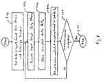
- FIG. 8 shows a flow chart for an exemplary decision process in a CDR.
- step S 200 the process compares a plurality of consecutive sampled data. The process goes to step S 202 .
- Step S 202 the process determines whether an edge transition is present. As discussed above, an edge transition is detected when a pair of consecutive sampled data bits have different values. If an edge transition is detected, the process goes to step S 204 ; otherwise the process goes to step S 214 .
- step S 204 the process determines whether fast-lock mode is enabled. If enabled, the process goes to step S 206 ; otherwise the process goes to step S 208 .
- the fast-lock process changes a phase step size so that convergence to the synchronization point may be achieved at a faster rate.
- step S 206 the process determines an appropriate phase step size.
- the phase step size for the fast-lock mode may be set to a fixed value such as 45 degrees, for example.
- the process may adjust the step size based on specific parameters such as the number of contiguous clock cycles the CDR is in the fast-lock mode, or the number of times the fast-lock mode was used so far during the current communication.
- the process goes to step S 208 .
- step S 208 the process determines whether a phase lag or phase lead condition was detected.
- a phase lead condition indicates that the sample point 0 is occurred before the edge transition and a phase lag condition indicates that the sample point 0 occurred after the edge transition. If a phase lag condition is detected, the process goes to step S 212 ; otherwise the process goes to step S 210 .
- step S 210 the process increments the counter 54 by the current step size; and in step S 212 , the process decrements the counter 54 by the current step size and the process goes to step S 214 .
- the step S 214 the process determines whether the communication is completed. If completed, the process goes to step S 216 and ends; otherwise the process returns to step S 200 .
Landscapes
- Engineering & Computer Science (AREA)
- Computer Networks & Wireless Communication (AREA)
- Signal Processing (AREA)
- Synchronisation In Digital Transmission Systems (AREA)
Abstract
Description
| TABLE 1 | |||||
| Clk0 | | Clk2 | Clk3 | ||
| 3200 | Sampling Point | 0 | |
|
|
|
| 1600 | Sampling Point | 0 | |
|
|
|
| 800 | Sampling Point | 0, 2 | Not Used | |
Not Used | |
| 400 MHz | Sampling Point 0-3 | Not Used | Not Used | Not Used | ||
Claims (21)
Priority Applications (1)
| Application Number | Priority Date | Filing Date | Title |
|---|---|---|---|
| US10/828,318 US7349509B2 (en) | 2004-04-21 | 2004-04-21 | Multi rate clock data recovery based on multi sampling technique |
Applications Claiming Priority (1)
| Application Number | Priority Date | Filing Date | Title |
|---|---|---|---|
| US10/828,318 US7349509B2 (en) | 2004-04-21 | 2004-04-21 | Multi rate clock data recovery based on multi sampling technique |
Publications (2)
| Publication Number | Publication Date |
|---|---|
| US20050238126A1 US20050238126A1 (en) | 2005-10-27 |
| US7349509B2 true US7349509B2 (en) | 2008-03-25 |
Family
ID=35136408
Family Applications (1)
| Application Number | Title | Priority Date | Filing Date |
|---|---|---|---|
| US10/828,318 Active 2026-03-12 US7349509B2 (en) | 2004-04-21 | 2004-04-21 | Multi rate clock data recovery based on multi sampling technique |
Country Status (1)
| Country | Link |
|---|---|
| US (1) | US7349509B2 (en) |
Cited By (8)
| Publication number | Priority date | Publication date | Assignee | Title |
|---|---|---|---|---|
| US20070002989A1 (en) * | 2005-06-30 | 2007-01-04 | Hongjiang Song | Method and system for link jitter compensation including a fast data recovery circuit |
| US20080043826A1 (en) * | 2006-08-21 | 2008-02-21 | Rafael Castro | Sampling Mechanism for Data Acquisition Counters |
| US20080201597A1 (en) * | 2006-08-24 | 2008-08-21 | Altera Corporation | Write-leveling implementation in programmable logic devices |
| US20100054382A1 (en) * | 2008-08-27 | 2010-03-04 | Ryan John Kinnerk | Recovering Data From An Oversampled Bit Stream With A Plesiochronous Receiver |
| CN103621005A (en) * | 2011-06-30 | 2014-03-05 | 英特尔移动通信有限责任公司 | Enhanced phase discriminator for fast phase alignment |
| US9323699B2 (en) | 2009-08-03 | 2016-04-26 | National Instruments Corporation | Methods for data acquisition systems in real time applications |
| US9673963B1 (en) | 2016-04-12 | 2017-06-06 | Keyssa Systems, Inc. | Multi-protocols and multi-data rates communications |
| US10063365B1 (en) | 2017-03-10 | 2018-08-28 | Keyssa Systems, Inc. | Re-timer network insertion |
Families Citing this family (21)
| Publication number | Priority date | Publication date | Assignee | Title |
|---|---|---|---|---|
| US8050373B2 (en) | 2004-06-28 | 2011-11-01 | Broadcom Corporation | Phase interpolator based transmission clock control |
| US8085880B2 (en) * | 2004-12-23 | 2011-12-27 | Rambus Inc. | Amplitude monitor for high-speed signals |
| US7672416B2 (en) * | 2005-03-30 | 2010-03-02 | Alcatel-Lucent Usa Inc. | High-speed serial transceiver with sub-nominal rate operating mode |
| US7724857B2 (en) * | 2006-03-15 | 2010-05-25 | Agere Systems Inc. | Method and apparatus for improving linearity in clock and data recovery systems |
| US20120087418A1 (en) * | 2008-01-18 | 2012-04-12 | Agency For Science, Technology And Research | Communication Device and Method of Determining a Ranging Value in the Communication Device |
| US7929644B2 (en) * | 2008-02-01 | 2011-04-19 | Panasonic Corporation | Instant-acquisition clock and data recovery systems and methods for serial communications links |
| JP2010147558A (en) * | 2008-12-16 | 2010-07-01 | Renesas Electronics Corp | Clock data recovery circuit |
| US8396180B2 (en) * | 2008-12-18 | 2013-03-12 | Kawasaki Microelectronics America Inc. | High jitter tolerant phase comparator |
| US8699647B2 (en) * | 2009-06-23 | 2014-04-15 | Intel Mobile Communications GmbH | Fast phase alignment for clock and data recovery |
| TWI436219B (en) * | 2011-04-19 | 2014-05-01 | Raydium Semiconductor Corp | Sampling phase selection module for a stream of data bits |
| US9076325B1 (en) * | 2013-05-13 | 2015-07-07 | Kiomars Anvari | Wireless sensor with digital detector |
| TWI519119B (en) * | 2014-04-17 | 2016-01-21 | 創意電子股份有限公司 | Clock data recovery circuit and method |
| US9379880B1 (en) * | 2015-07-09 | 2016-06-28 | Xilinx, Inc. | Clock recovery circuit |
| US9800438B1 (en) * | 2016-10-25 | 2017-10-24 | Xilinx, Inc. | Built-in eye scan for ADC-based receiver |
| TWI658700B (en) * | 2018-07-16 | 2019-05-01 | 創意電子股份有限公司 | Integrated circuit, multi-channels transmission apparatus and signal transmission method thereof |
| KR102509984B1 (en) * | 2018-10-12 | 2023-03-14 | 삼성전자주식회사 | Integrated circuit detecting frequency and phase of clock signal and clock and data recovery circuit including the same |
| TWI690162B (en) | 2019-08-30 | 2020-04-01 | 瑞昱半導體股份有限公司 | Clock data recovery apparatus and method |
| US11269532B2 (en) * | 2019-10-30 | 2022-03-08 | EMC IP Holding Company LLC | Data reduction by replacement of repeating pattern with single instance |
| US11038602B1 (en) | 2020-02-05 | 2021-06-15 | Credo Technology Group Limited | On-chip jitter evaluation for SerDes |
| US10992501B1 (en) | 2020-03-31 | 2021-04-27 | Credo Technology Group Limited | Eye monitor for parallelized digital equalizers |
| US10892763B1 (en) * | 2020-05-14 | 2021-01-12 | Credo Technology Group Limited | Second-order clock recovery using three feedback paths |
Citations (4)
| Publication number | Priority date | Publication date | Assignee | Title |
|---|---|---|---|---|
| US5757297A (en) * | 1996-06-07 | 1998-05-26 | International Business Machines Corporation | Method and apparatus for recovering a serial data stream using a local clock |
| US20040247049A1 (en) * | 2003-06-09 | 2004-12-09 | Maddux John T. | Extending PPM tolerance using a tracking data recovery algorithm in a data recovery circuit |
| US20050069071A1 (en) * | 2003-09-30 | 2005-03-31 | Dennis Kim | Clock-data recovery ("CDR") circuit, apparatus and method for variable frequency data |
| US20050180536A1 (en) * | 2004-02-17 | 2005-08-18 | Payne Robert F. | Interpolator based clock and data recovery (CDR) circuit with digitally programmable BW and tracking capability |
-
2004
- 2004-04-21 US US10/828,318 patent/US7349509B2/en active Active
Patent Citations (4)
| Publication number | Priority date | Publication date | Assignee | Title |
|---|---|---|---|---|
| US5757297A (en) * | 1996-06-07 | 1998-05-26 | International Business Machines Corporation | Method and apparatus for recovering a serial data stream using a local clock |
| US20040247049A1 (en) * | 2003-06-09 | 2004-12-09 | Maddux John T. | Extending PPM tolerance using a tracking data recovery algorithm in a data recovery circuit |
| US20050069071A1 (en) * | 2003-09-30 | 2005-03-31 | Dennis Kim | Clock-data recovery ("CDR") circuit, apparatus and method for variable frequency data |
| US20050180536A1 (en) * | 2004-02-17 | 2005-08-18 | Payne Robert F. | Interpolator based clock and data recovery (CDR) circuit with digitally programmable BW and tracking capability |
Cited By (15)
| Publication number | Priority date | Publication date | Assignee | Title |
|---|---|---|---|---|
| US20070002989A1 (en) * | 2005-06-30 | 2007-01-04 | Hongjiang Song | Method and system for link jitter compensation including a fast data recovery circuit |
| US7792232B2 (en) * | 2005-06-30 | 2010-09-07 | Intel Corporation | Method and system for link jitter compensation including a fast data recovery circuit |
| US20080043826A1 (en) * | 2006-08-21 | 2008-02-21 | Rafael Castro | Sampling Mechanism for Data Acquisition Counters |
| US8176351B2 (en) | 2006-08-21 | 2012-05-08 | National Instruments Corporation | Sampling mechanism for data acquisition counters |
| US8671303B2 (en) | 2006-08-24 | 2014-03-11 | Altera Corporation | Write-leveling implementation in programmable logic devices |
| US20080201597A1 (en) * | 2006-08-24 | 2008-08-21 | Altera Corporation | Write-leveling implementation in programmable logic devices |
| US8122275B2 (en) * | 2006-08-24 | 2012-02-21 | Altera Corporation | Write-leveling implementation in programmable logic devices |
| US20100054382A1 (en) * | 2008-08-27 | 2010-03-04 | Ryan John Kinnerk | Recovering Data From An Oversampled Bit Stream With A Plesiochronous Receiver |
| US9323699B2 (en) | 2009-08-03 | 2016-04-26 | National Instruments Corporation | Methods for data acquisition systems in real time applications |
| US9996407B2 (en) | 2009-08-03 | 2018-06-12 | National Instruments Corporation | Methods for data acquisition systems in real time applications |
| US10621025B2 (en) | 2009-08-03 | 2020-04-14 | National Instruments Corporation | Methods for data acquisition systems in real time applications |
| CN103621005A (en) * | 2011-06-30 | 2014-03-05 | 英特尔移动通信有限责任公司 | Enhanced phase discriminator for fast phase alignment |
| CN103621005B (en) * | 2011-06-30 | 2017-08-25 | 英特尔德国有限责任公司 | The enhanced phase discriminator alignd for fast phase |
| US9673963B1 (en) | 2016-04-12 | 2017-06-06 | Keyssa Systems, Inc. | Multi-protocols and multi-data rates communications |
| US10063365B1 (en) | 2017-03-10 | 2018-08-28 | Keyssa Systems, Inc. | Re-timer network insertion |
Also Published As
| Publication number | Publication date |
|---|---|
| US20050238126A1 (en) | 2005-10-27 |
Similar Documents
| Publication | Publication Date | Title |
|---|---|---|
| US7349509B2 (en) | Multi rate clock data recovery based on multi sampling technique | |
| US4821297A (en) | Digital phase locked loop clock recovery scheme | |
| US9912469B2 (en) | Phase control block for managing multiple clock domains in systems with frequency offsets | |
| US9520883B2 (en) | Frequency detection circuit and reception circuit | |
| KR100913400B1 (en) | Serial transmitter and receiver, and communication method thereof | |
| JP4607666B2 (en) | Data sampling circuit and semiconductor integrated circuit | |
| US20070047686A1 (en) | Clock and data recovery circuit | |
| JP4893052B2 (en) | Receiver circuit and receiver circuit test method | |
| JP4808769B2 (en) | Method and apparatus for synchronizing data transferred over a multi-pin asynchronous serial interface | |
| US8259886B2 (en) | Communication apparatus | |
| US7453970B2 (en) | Clock signal selecting apparatus and method that guarantee continuity of output clock signal | |
| JPH07336342A (en) | Clock reproducing circuit | |
| US9887831B2 (en) | Clock data recovery circuit, integrated circuit including the same, and clock data recovery method | |
| US7194057B2 (en) | System and method of oversampling high speed clock/data recovery | |
| US8295423B2 (en) | System and method for clockless data recovery | |
| US8811559B1 (en) | Timing recovery circuit and receiver circuit including the same | |
| EP1113616B1 (en) | Method for recovering a clock signal in a telecommunications system and circuit thereof | |
| RU2271069C2 (en) | Method and circuit for synchronous data reception during high-speed data transfer from subscriber to central point in optical data transfer system | |
| US20070230646A1 (en) | Phase recovery from forward clock | |
| KR19990077789A (en) | Over-sampling type clock recovery circuit and the method of adjusting phsaes of clock signals thereof | |
| US8199869B2 (en) | Communication apparatus | |
| US6973149B2 (en) | Arrangement for capturing data | |
| US8139697B2 (en) | Sampling method and data recovery circuit using the same | |
| JP3973149B2 (en) | Data recovery circuit and data recovery method | |
| US7376528B2 (en) | Devices and methods for testing clock and data recovery devices |
Legal Events
| Date | Code | Title | Description |
|---|---|---|---|
| AS | Assignment |
Owner name: KAWASAKI LSI U.S.A., INC., CALIFORNIA Free format text: ASSIGNMENT OF ASSIGNORS INTEREST;ASSIGNORS:RIBO, JEROME;ROEDERER, BENOIT;REEL/FRAME:015264/0099 Effective date: 20040419 |
|
| STCF | Information on status: patent grant |
Free format text: PATENTED CASE |
|
| AS | Assignment |
Owner name: KAWASAKI MICROELECTRONICS AMERICA, INC., CALIFORNI Free format text: CHANGE OF NAME;ASSIGNOR:KAWASAKI LSI U.S.A., INC.;REEL/FRAME:025304/0065 Effective date: 20040510 |
|
| FEPP | Fee payment procedure |
Free format text: PAYOR NUMBER ASSIGNED (ORIGINAL EVENT CODE: ASPN); ENTITY STATUS OF PATENT OWNER: LARGE ENTITY |
|
| AS | Assignment |
Owner name: KAWASAKI MICROELECTRONICS, INC., JAPAN Free format text: ASSIGNMENT OF ASSIGNORS INTEREST;ASSIGNOR:KAWASAKI MICROELECTRONICS AMERICA, INC.;REEL/FRAME:025605/0535 Effective date: 20101216 |
|
| FPAY | Fee payment |
Year of fee payment: 4 |
|
| FPAY | Fee payment |
Year of fee payment: 8 |
|
| MAFP | Maintenance fee payment |
Free format text: PAYMENT OF MAINTENANCE FEE, 12TH YEAR, LARGE ENTITY (ORIGINAL EVENT CODE: M1553); ENTITY STATUS OF PATENT OWNER: LARGE ENTITY Year of fee payment: 12 |